
Graphite–metal composite electrodes with a tunable work function for use in optoelectronic devices†
Arul Varman
Kesavan
ab,
Atul C.
Khot
a,
Tukaram D.
Dongale
 ac,
Kyung Rock
Son
a,
Praveen C.
Ramamurthy
d and
Tae Geun
Kim
*a
ac,
Kyung Rock
Son
a,
Praveen C.
Ramamurthy
d and
Tae Geun
Kim
*a
aSchool of Electrical Engineering, Korea University, Seoul, 02841, Republic of Korea. E-mail: tgkim1@korea.ac.kr; Fax: +82 2 924 5119; Tel: +82 2 3290 3255
bDepartment of Physics & Nanotechnology, SRM Institute of Science & Technology, Kattankulathur, 603203, India
cSchool of Nanoscience and Biotechnology, Shivaji University, Kolhapur, 416 004, India
dDepartment of Materials Engineering, Indian Institute of Science, Bangalore, 560012, India
First published on 21st September 2022
Abstract
In electronic devices, the work function (WF) of the electrodes must be tailored to achieve a well-aligned Ohmic or Schottky contact. Low- and high-WF electrodes are typically used to ensure effective injection/extraction of electrons and holes. In this study, composite graphite–aluminum (G![[thin space (1/6-em)]](https://www.rsc.org/images/entities/char_2009.gif) :Al) and graphite–nickel (G:Ni) electrodes were deposited on a glass substrate using electron beam evaporation, and ambient pressure photoemission spectroscopy was conducted to evaluate the WF of the fabricated electrodes. The WF of the G:Al electrode was successfully tuned from 4.24 ± 0.047 eV to 5.10 ± 0.031 eV (a range of ∼0.9 eV) by increasing the graphite content. Similarly, the WF of the G:Ni composite electrode was tuned from 4.67 ± 0.041 eV to 5.11 ± 0.031 eV (a range of ∼0.4 eV). The shift in the WF in the composite graphite–metal electrodes could be explained by the formation of metal–metal (or semiconductor) junctions. The optical reflectance, sheet resistance, and morphology were also able to be tuned. The sheet resistance of the G:Al and G:Ni electrodes varied from 2.28 ± 0.03 Ω sq−1 to 80.05 ± 9.1 Ω sq−1 and from 4.92 ± 0.04 Ω sq−1 to 166.30 ± 4.1 Ω sq−1, respectively, while the total tunable reflectance was 53.77% and 45.70%, respectively. This research demonstrates a novel exploratory technique for tailoring the WF of hybrid graphite materials.
:Al) and graphite–nickel (G:Ni) electrodes were deposited on a glass substrate using electron beam evaporation, and ambient pressure photoemission spectroscopy was conducted to evaluate the WF of the fabricated electrodes. The WF of the G:Al electrode was successfully tuned from 4.24 ± 0.047 eV to 5.10 ± 0.031 eV (a range of ∼0.9 eV) by increasing the graphite content. Similarly, the WF of the G:Ni composite electrode was tuned from 4.67 ± 0.041 eV to 5.11 ± 0.031 eV (a range of ∼0.4 eV). The shift in the WF in the composite graphite–metal electrodes could be explained by the formation of metal–metal (or semiconductor) junctions. The optical reflectance, sheet resistance, and morphology were also able to be tuned. The sheet resistance of the G:Al and G:Ni electrodes varied from 2.28 ± 0.03 Ω sq−1 to 80.05 ± 9.1 Ω sq−1 and from 4.92 ± 0.04 Ω sq−1 to 166.30 ± 4.1 Ω sq−1, respectively, while the total tunable reflectance was 53.77% and 45.70%, respectively. This research demonstrates a novel exploratory technique for tailoring the WF of hybrid graphite materials.
1. Introduction
The work function (WF) is a key component in the analysis of the electronic properties of materials. The WF refers to the energy needed to take an electron from the Fermi energy level (EF) to the vacuum energy level (Evac), that is, WF = Evac − EF. The WF of a material can be determined using thermionic emission, photoemission, field emission, and contact potential difference approaches. In addition, numerous methods have been developed to tune the WFs of electrodes,1–3 and these can be divided into two main categories: physical and chemical modification. Using these methods, the WF can be changed by only a few Angstroms from the surface to the bulk region. Physical methods such as the modification of the surface roughness can help tune the WF, although only within a small range. For example, by increasing the surface roughness of materials with lightning (Cu and Ag) and anti-lightning rod (Al and Mg) effects, the WF can be decreased and increased, respectively. In particular, the weak interaction between valence electrons and nuclei on rough surfaces facilitates the escape of electrons from the surface, resulting in a low WF.4The introduction of small molecules or a non-conjugated polyelectrolyte interface layer can also change the electrical field distribution between the semiconductor and the electrode. This electric field redistribution leads to Fermi level pinning, electric double-layer formation, charge transfer, spontaneous dipole orientation, spontaneous interfacial dipole orientation,5 electron pushback (repulsion), and interface dipole formation. These effects are associated with changes in the electrode WF. The degree of this shift in the electrode WF depends on the strength of the electric field and the choice of polyelectrolyte. Acidic and basic polyelectrolytes result in dipole formation pointing inward and outward from the electrode, leading to an increase and decrease in the WF, respectively. Nonionic polyelectrolytes do not lead to a change in the WF due to null dipole formation. Notably, chemical modification influences electrode stability in the long term.
In most electronic devices, metal electrodes such as gold, silver, copper, nickel, and aluminum are routinely used, the WF of which must be tuned. Alkanethiols and other polymers and small molecules are widely used to modify the WF of Au,6 Ag,7 and Cu. The self-assembled monolayer (SAM) of alkanethiol on Au can lead to a charge transfer of less than 0.05 eV. However, the thiol (R–S⋯H) anchor group of alkanethiol adsorbed onto the Au surface leads to the formation of Au–S bonds. This observation suggests that the WF shift is primarily associated with the dipole movement of individual molecules, while gauche defects unavoidably occur in SAMs. Compared to isolated molecules, the dipole moment decreases (known as the depolarization effect) in the SAM. However, the intensity of this effect is negligible, and it is thus not considered in many practical applications.8–10
The WF of an electrode can also be modified using doping, the preparation of metal alloys, and the engineering of the crystallographic orientation. The WF of metals is an anisotropic function of the crystallographic orientation of the grains. This anisotropy is associated with the variation in the atomic packing density with the crystallographic orientation. A surface with a low atomic packing density exhibits a low WF, while a high atomic packing density leads to a high WF. The atomic packing density of many face-centered cubic (fcc) metals (Ni, Cu, and Ag) varies according to the crystallographic orientation in the following manner: (110)fcc < (001)fcc < (111)fcc. Moreover, based on the crystallographic orientation, the atomic packing fraction increases in the following order: (111)bcc < (001)bcc < (110)bcc. Therefore, the surface free energy is inversely related to the WF, leading to the following trend in the surface free energy for fcc and body-centered cubic (bcc) metals: γ(110)fcc > γ(001)fcc > γ(111)fcc and γ(111)bcc > γ(001)bcc > γ(110)bcc. The anisotropic WF of many metals can be attributed to the presence of p- and d-orbitals, which are anisotropically distributed near the Fermi surface. For Al, the p-orbital is directionally dependent, leading to anisotropic characteristics, while s–d orbital hybridization causes anisotropy in metals such as Cu and Au. In principle, many materials exhibit an anisotropic WF due to the presence of asymmetric orbitals near the Fermi surface.11,12 On the other hand, the properties of graphite can be characterized by the type of hybridization of carbon in graphite (sp3, sp2, and sp1). Higher amounts of sp3 hybridized bonds in graphite results in diamond-like carbon, which is less conductive.
Based on these considerations, this study aimed to systematically investigate the structural, optical, morphological, and electrical properties of composite graphite–metal (graphite–aluminum [G:Al] and graphite–nickel [G:Ni]) electrodes prepared using electron beam (e-beam) evaporation. The WF of the G:Al and G:Ni electrodes was tuned by modifying the electrode composition. Using the composite electrodes, the unique physical and chemical properties of the parent materials (i.e., graphite, Al, and Ni) were able to be exploited.
2. Experimental details
2.1. Materials
Graphite particles with an average particle size of ∼8 mm (∼99.9%), Al nanoparticles (NPs, 99.9%, 40 nm), and Ni NPs (99.9%, 40 nm) were purchased from US Research Nanomaterials, Inc.2.2. Preparation of the composite pellets and e-beam evaporation
The graphite particles and Al/Ni NPs were well mixed in various composition ratios to attain a homogeneous mixture. The composite materials (G:Al/G:Ni) were compressed to produce pellets, which were placed in a crucible and loaded into an e-beam chamber (e-beam evaporator model KVE-E2003L, Korean Vacuum Tech., Ltd, South Korea). The DC output voltage was set at 7 kV with a probe current of 80–100 mA. Evaporation was conducted at the pressure level of <5.5 × 10⁻⁵ mbar. The electrode materials were deposited on a clean glass slide that had been sonicated for 10 min each in water, acetone, methanol, and isopropanol. The substrate temperature was maintained at room temperature (25 °C) via water circulation. Electrodes with a thickness of ∼100–150 nm were fabricated (evaporation rate ∼ 0.5–3.0 Å s−1). The thickness of the deposited films was evaluated using a surface profiler (KLA Tencor-Alpha-step IQ). The following samples were produced (where G denotes graphite and the number represents the % composition for that element): G1:Al9, G2:Al8, G3:Al7, G4:Al6, G5:Al5, G6:Al4, G7:Al3, G8:Al2, G9:Al1, G1:Ni9, G2:Ni8, G3:Ni7, G4:Ni6, G5:Ni5, G6:Ni4, G7:Ni3, G8:Ni2, and G9:Ni1.
2.3. Electrical and work function characterization
Four-point probe method was used to measure the sheet resistance (Rs) of the samples (area 1.5 mm × 1.5 mm). I–V measurements were conducted using a Keithley 4200A-SCS measurement system. The conductivity of the samples was measured by positioning the probes at a distance of 2 cm. The WF of the samples was measured using ambient pressure photoemission spectroscopy (APS). A high-intensity deuterium (D2) lamp was employed to eject the photoelectrons from the electrode surface. The wavelength of the D2 light could be tuned from 180 nm (3.4 eV) to 340 nm (7.0 eV) using a deep UV light source. To generate the photoelectrons, a circular D2 beam was employed to illuminate the sample surface. The photoelectrons were collected by a circular (diameter ∼ 2 mm) gold collector probe. To maximize the collection of the photoelectrons generated via D2 illumination, a Au tip was centrally aligned with the circular UV light spot. Photoelectrons were acquired at a resolution within the contact potential difference of 0.001–0.003 eV and a WF resolution of ≤0.003 eV. During the measurement process, a nitrogen (purity ∼99.999%) environment was maintained. The nitrogen was purged (∼60 mL s−1) to maintain an oxygen level <1% within the measurement chamber.We analyzed the photocurrent/photoelectron spectra in accordance with the photon energy using the Fowler theory to determine the WF. Fowler's theory can be expressed as R ∞ (Eph − hυ0)2, where R is the obtained photocurrent (electrons) per incident photon, Eph is the incident photon energy, h is Planck's constant, and υ0 is the threshold frequency. The density of states (DOS) near the Fermi energy level considerably influences the mechanical, chemical, and physical properties of a material. To determine the DOS for the nanocomposite electrodes, the photocurrent/photoelectron intensity (Y) was plotted against the photon energy (E) was done. The plot of dY/dE against the photon energy yielded the DOS distribution.13
2.4. Structural, optical, and morphological characterization
The structural properties of the composite G:Al and G:Ni samples were characterized using X-ray diffraction (XRD). Diffraction measurements were taken using a Rigaku SmartLab XRD instrument. The current and voltage in the X-ray generation tube were 200 mA and 45 kV, respectively. Cu was employed as the X-ray target to induce Kα radiation with a wavelength of 1.54 Å. The Raman spectra of the samples were obtained using a LabRam ARAMIS IR2 system. Diode laser emitting with a center wavelength of 532 nm was used to probe the samples. The spatial resolution of the instrument was 1 μm, and the clearance between the sample and the lens system was 0.26 mm.
The absorption, transmittance, and reflectance of the neat graphite and composite graphite–Al/Ni electrodes were measured using a UV spectrometer (PerkinElmer Lambda 35). The total reflectance spectra of the composite electrodes were obtained using the UV spectrometer with an integrating sphere setup. The equation 1-R-T = A was used. An optical microscope (Olympus BX51M) was used to examine the composite electrode surface. Atomic force microscopy (Park Systems XE series) was employed in non-contact mode to analyze the root mean square (RMS) roughness and the surface morphology.
3. Results and discussion
3.1. Structural properties of thecomposite electrodes
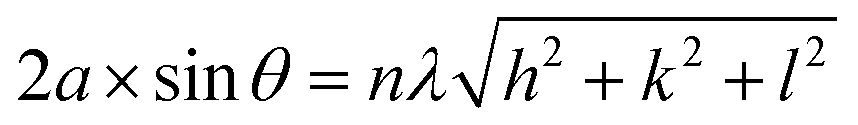
:Al and G:Ni films were examined using XRD. The neat graphite thin film had an amorphous graphite structure and exhibited a broad diffraction peak at 22° owing to the short-range crystalline order of amorphous graphite film. The crystallite size of the Al and Ni in the composite films was calculated using the Scherrer formula (eqn (1)) from the full width at half maximum (FWHM) of the (111) peak. According to the Scherrer derivation, peak broadening can be attributed to a reduction in the crystallite size and lattice-strain-induced broadening. However, the crystallite size of Al and Ni was determined by assuming that the XRD peak broadening was primarily caused by a reduction in the crystallite size; the lattice-strain-induced broadening was considered negligible. The measured FWHM (2θ) for the (111) peak and corresponding crystallite sizes for the G:Al and G:Ni composites are presented in Tables S1 and S2 (ESI†), respectively. A shift in the (111) peak was observed for the G:Al and G:Ni nanocomposites, indicating a modification to the lattice parameters. A larger variation in the peak shift corresponded to a larger change in lattice parameter a (eqn (2)). The calculated FWHM (2θ) and crystallite sizes of the G:Al and G:Ni electrodes are summarized in Tables S3 and S4 (ESI†), respectively. The XRD spectra (10–90°) for the G:Al and G:Ni composite electrodes are presented in Fig. 1a and b, respectively.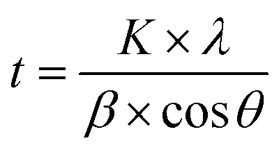 | (1) |
 | (2) |
:Al and G:Ni electrodes were quantified using eqn (3) and (4), respectively:14–16 | (3) |
 | (4) |
:Al electrodes, the diffraction intensity of these planes decreased. The diffraction peaks at 38.5°, 44.74°, and 65.13° were indicative of the fcc structure of the Al phase.17 However, the (111) peak positions shifted to higher 2θ values as the graphite content increased in the G:Al composite (from 38.5° for Al to 38.6523° for G5:Al5). According to eqn (2), a larger 2θ corresponds to a smaller lattice constant a. In addition, the FWHM also increased as the graphite content in the composite electrode increased (from 0.7553 for G1:Al9 to 0.9507 for G5:Al5). In other words, the Al crystallite size decreased with an increasing graphite content (from 11.65 nm for G1:Al9 to 9.25 nm for G5:Al5). A smaller ratio of Al in the G:Al source corresponded to a lower Al vapor density and growth rate, resulting in a smaller crystallite size. Regardless of the G:Al ratio, the intensity of the diffraction peaks had the following order: (111) > (200) > (220) > (311). A broad diffraction peak was also observed at a 2θ angle of 22° due to the random presence of short-range ordering in the graphite and the contribution of the Al grain boundaries (Fig. 1a).18 As the graphite content increased in the G:Al composite, both interplanar spacing b and lattice constant a decreased (Table S3, ESI†), suggesting a contraction in the unit cell volume.
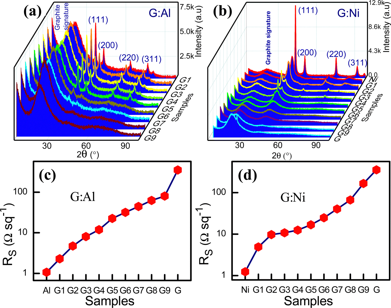 | ||
| Fig. 1 XRD spectra for the composite (a) G:Al and (b) G:Ni electrodes. Sheet resistance for the (c) G:Al and (d) G:Ni electrodes on a log scale. | ||
Fig. 1b displays the XRD spectra for the G:Ni electrodes and Ni (fcc). The calculated 2θ, FWHM, and crystallite size for these electrodes are also presented in Table S4 (ESI†), and the variation with respect to the graphite content is shown in Fig. S2a–c (ESI†). As the graphite content increased, the 2θ of the (111) peak shifted to lower values (from 45.02° for Ni to 43.68° for G8:Ni2). This decrease in 2θ of ∼1.34° was related to an increase in the lattice constant a for Ni (eqn (2)), which indirectly indicated a change in the unit cell volume (V). The FWHM of Ni and G8:Ni2 was 0.66° and 6.29°, respectively, demonstrating that the crystallite size for G8:Ni2 (1.4 nm) was smaller than that for the Ni (13.5 nm) electrode. The variation in 2θ, FWHM, and crystallite size according to the G:Ni ratio is presented in Fig. S2d–f (ESI†). The variation in the lattice constant and the interplanar spacing was calculated for the composite electrodes (Table S4, ESI†). For the G:Ni electrodes, as the graphite content increased, both interplanar spacing d and the lattice constant a increased.
3.2. Electrical properties of the composite electrodes
:Al composites, the sheet resistance increased due to the low conductivity of graphite. The sheet resistance of the G:Al composites was between that for Al and graphite (2.284 ± 0.03 Ω sq−1 for G1:Al9 and 80.052 ± 9.11 Ω sq−1 for G9:Al1). The sheet resistance of the composite G:Al electrode could be tuned by ∼78 Ω sq−1. The electrode with 10% Al and 90% graphite had a 77% lower sheet resistance than that of pure graphite. In contrast, the electrode with 10% graphite and 90% Al had a 50% higher sheet resistance.22,23 The variation in the sheet resistance according to the Al and Ni content is presented in Fig. 1c and d, respectively. The I–V characteristics (Fig. S4a and b, ESI†) and conductivity (Fig. S4c and d, ESI†) of the G:Al and G:Ni electrodes are also plotted.
Due to the mechanisms described above, the addition of graphite to the Ni electrode led to an increased Rs. The sheet resistance of various G:Ni composite electrode is presented in Table S2 (ESI†). The pure Ni electrode exhibited a sheet resistance of 1.244 ± 0.005 Ω sq−1 (d-119.1 ± 11 nm), while the composite electrodes had a sheet resistance range of 161 Ω sq−1 (from 4.903 ± 0.043 Ω sq−1 for G1:Ni9 to 166.3 ± 4.101 Ω sq−1 for G9:Ni1). For the G:Al and G:Ni electrodes, regardless of their surface defects or porosity, the sheet resistance increased with increasing graphite content due to the low conductivity of graphite. The electrical resistivity (eqn (5)) and conductivity (eqn (6)) were determined using Rs, while the factors influencing the DC conductivity of the G:Al and G:Ni composite electrodes are summarized in eqn (7).
| ρ = Rsd | (5) |
 | (6) |
 | (7) |
:Al and G:Ni electrodes, the total variation in the RMS roughness was 0.32–5.26 nm and 0.22–1.40 nm, respectively.
In general, charge transfer is a spontaneous process that occurs at any interface between two materials that are in contact (metals, semiconductors, or insulators). The charge transfer mechanism across the G:Al and G:Ni interfaces and the change in the WF in these composite electrodes can be understood in terms of metal–metal (or semiconductor) junction formation and the associated band energy structure (Fig. S6a–e, ESI†). Metal–metal junctions are usually formed between two conducting materials. When a metal–metal (or semiconductor) Ohmic contact is formed between materials with dissimilar WFs, a contact potential is generated. Electrons in the low-WF metal tunnel into the high-WF metal until the Fermi level of both metals is similar at equilibrium (i.e., no external bias at a given temperature). The electrons from the high-WF metal also flow to the low-WF metal and occupy empty energy levels, resulting in a minimum Helmholtz free energy. At equilibrium, a new EF is generated that differs from that of the individual metals. This process results in a positive pole in the high-WF metal and a negative pole in the low-WF metal. Consequently, at equilibrium, a contact potential is generated between the metals, the magnitude of which depends on the difference in the WF of the contacting metals.31,32Fig. 2a and b present a schematic overview of the graphite–Al/Ni system before and after junction formation, respectively. Similarly, Fig. 2c–e display the charge density distribution, electric field distribution, and electric potential at the junction, respectively. The change in the WF of the composite electrodes according to the graphite content is shown in Fig. 2f and g, respectively. In both cases, the WF increased as the graphite content increased in the G:Al and G:Ni electrodes. The difference in WF between the electrodes can be explained by the formation of metal–metal (or semiconductor) Ohmic junctions. The WF of the neat Al and graphite electrodes was 4.24 ± 0.047 eV and 5.10 ± 0.031 eV, respectively (Fig. 2f). In the G:Al composites, however, the electrons flowed from Al to the graphite, thus generating a new Fermi level that depended on the ratio of Al and graphite.
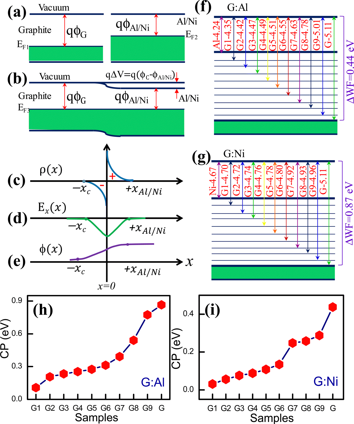 | ||
| Fig. 2 Graphite–Al/Ni composites (a) before and (b) after junction formation. (c) Space charge density distribution, (d) electric field distribution, (c) charge density distribution and (d) electric field, (e) electric potential at the junction. WF of various composite (f) G:Al and (g) G:Ni electrodes and the contact potential (CP) of (h) G:Al and (i) G:Ni electrodes. | ||
The Fermi level alignment in these composites can also be explained based on the graphite and Al phase distributions within the composite film. The phase distributions can be divided into three categories: (i) low graphite content, (ii) low Al (or high graphite) content, and (iii) an equal ratio of graphite and Al. In the electrodes with a low graphite content, such as G1:Al9 (4.353 eV), G2:Al8 (4.421 eV), G3:Al7 (4.478 eV), and G4:Al6 (4.499 eV) (Table S1, ESI†), a larger region is covered by the Al phase and an extremely small region is occupied by graphite. In this configuration, the graphite is assumed to be embedded in the Al matrix like a series of islands (Fig. S7, ESI†), which generates more electron-donating states (i.e., the graphite boundary area) and fewer electron-accepting empty states (i.e., the Al boundary area). Therefore, only some of the electrons from Al can tunnel into the low-energy states of graphite at equilibrium. Nanoscale metal–metal (or semiconductor) Ohmic junctions form, followed by electron transfer. In other words, the volume fraction of the active interfacial area across the graphite and Al is low, thus only a marginal change in the WF is observed for the electrodes with a low Al content.
The change in the contact potential (ΔV) for the G1:Al9, G2:Al8, G3:Al7, G4:Al6, G5:Al5, G6:Al4, G7:Al3, G8:Al2, G9:Al1 and G electrodes is presented in Fig. 2h. The actual contact potential between graphite and Al is ∼0.9 eV, whereas the contact potential for the composites was less than this. A similar charge transfer mechanism was expected to occur in the G:Ni composite electrode. Fig. 2g and i show the difference in the WF and contact potential, respectively, between the G:Ni composite electrodes. The measured WF for the pristine Ni and graphite electrodes was 4.673 ± 0.041 eV and 5.111 ± 0.031 eV, respectively. For the C:Ni composite electrode system, the contact potential (ΔV) and tunable WF range was approximately 0.5 eV. In principle, the volume fraction of the active interfacial boundary formed between graphite and Ni dictated the change in the WF.
The LDOS, which is the DOS primarily associated with the valence band electrons, is the number of electronic states present in the unit energy range. The energy distribution and carrier concentration can be obtained from the DOS. The LDOS near the Fermi energy level of materials considerably influences the physical and chemical properties of a material.13 In this study, the LDOS was derived from the wavelength-dependent photoelectron emission spectra of the composite electrodes. Fig. 3a and b present the photoemission spectra for the G:Al and G:Ni electrodes, respectively, while the local DOS (LDOS; the valence band DOS) of the G:Al and G:Ni electrodes is presented in Fig. 3c and d, respectively, with the specific values summarized in Table S5 (ESI†). As the graphite content in the G:Al and G:Ni electrodes increased, the LDOS state decreased. The LDOS corresponding to the Fermi energy is the LDOS that is associated with the energy in the LDOS state plot. Thus, the DOS corresponding to the Fermi energy can be estimated based on the x-axis on the LDOS plot. The spectra for the variation in the integrated LDOS with the energy for the G:Al and G:Ni electrodes are displayed in Fig. S8a and b (ESI†), respectively, while the composition-dependent LDOS for the G:Al and G:Ni electrodes are presented in Fig. S8c and d (ESI†), respectively.
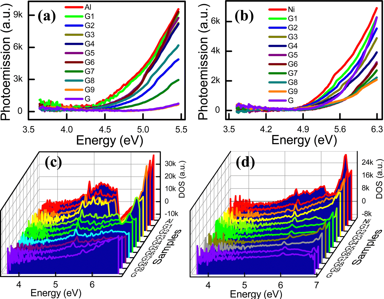 | ||
| Fig. 3 Photoemission spectra of the (a) G:Al and (b) G:Ni electrodes. Local density of states of the (c) G:Al and (d) G:Ni electrodes. | ||
3.3. Optical properties of the composite electrodes
The total reflectance of the hybrid electrodes was measured in the 200–1000 nm wavelength range (Fig. 4). The pristine Al electrode (∼78.73%R) exhibited a higher reflectance than the neat graphite (∼24.96%R) electrode. Therefore, in the composite G:Al electrodes, the total possible tunable reflectance (Δ%R) was ∼49.77%R. A target %R within this range can be achieved using a hybrid electrode with a suitable G:Al composition. Specifically, by increasing the graphite or Al content in the G:Al electrodes, %R can be decreased or increased, respectively. The reflectance spectra of the G:Al electrodes with various graphite to Al ratios are presented in Fig. 4a. For the neat Ni electrode, the reflectance was 70.66%R, while the tunable range for %R for a 100 nm-thick G:Ni electrode was approximately 45.7%R. The neat Ni electrode exhibited a higher reflectance than the neat G electrode (24.96%R). By increasing the graphite and Ni content in the G:Ni composite electrode, the %R can be decreased and increased, respectively (Fig. 4b).33 The average reflectance for the G:Al and G:Ni electrodes with increasing graphite content is presented in Fig. S9a and b (ESI†), respectively, while the plasmonic absorption of the G9:Al1 sample is presented in Fig. S9c (ESI†).
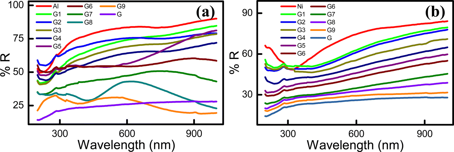 | ||
| Fig. 4 Optical reflectance spectra of (a) G:Al and (b) G:Ni electrodes. | ||
3.4. Morphology of the composite electrodes
The surface morphology of the G:Al and G:Ni electrodes was examined using optical micrographs and AFM. The optical micrographs were taken at a magnification of 5X. The surface texture of the Al and Ni electrodes was flat and it appeared to be free of pinholes. For both types of electrode, the number of pinholes increased with increasing graphite content. Furthermore, as the graphite content increased in the G:Al/G:Ni electrodes, the graphite phase grew, shown in the optical micrographs as a dark region. This increase in the dark phase suggests an increased domain size for graphite. In addition, island-type growth was observed in the films with high graphite levels of G:Al and G:Ni (Fig. S7, ESI†), while the distribution of graphite in the G:Al/G:Ni electrodes (black: graphite; gray: Al/Ni), with low (Fig. S6a, ESI†), medium (Fig. S6b, ESI†) and high graphite content (Fig. S6c, ESI†) is also schematically illustrated. Fig. S6d (ESI†) presents a close view of the schematic representation of the G:Al/G:Ni interface and Fig. S6e (ESI†) presents the Fermi energy and WF of Al, Ni, and G.
The surface morphology and RMS roughness of the G:Al and G:Ni electrodes were also examined using AFM in noncontact mode (Fig. 5). As the Al content in the G:Al electrodes increased, larger grains appeared on the surface (Fig. 5: G1:Al9, G2:Al8, G3:Al7, G4:Al6, G5:Al5, G6:Al4, G7:Al3, G8:Al2, G9:Al1). Though the RMS roughness of the G:Al electrodes varied with the Al content, the maximum roughness was 10 nm (Fig. S10a, ESI†). The average thickness of the G:Al and G:Ni electrodes is presented in Fig. S10c and d (ESI†). The difference in the crystallite size for the G:Al electrodes is summarized in Table S3 (ESI†). Similar trends were also noted for the G:Ni composite electrode (Fig. 5: G1:Ni9, G2:Ni8, G3:Ni7, G4:Ni6, G5:Ni5, G6:Ni4, G7:Ni3, G8:Ni2, G9:Ni1). In the composite G:Al/G:Ni electrodes, the graphite was amorphous in nature, whereas Al and Ni were in crystalline form. The difference in the crystallite size for the G:Ni electrodes is given in Table S4 (ESI†), while the RMS roughness obtained from AFM is listed in Table S1 and S2 (ESI†). Fig. S10b (ESI†) displays the average RMS roughness for the G:Ni electrodes and AFM images of the Ni electrode, Al electrode and graphite film are presented in Fig. S11 (ESI†).
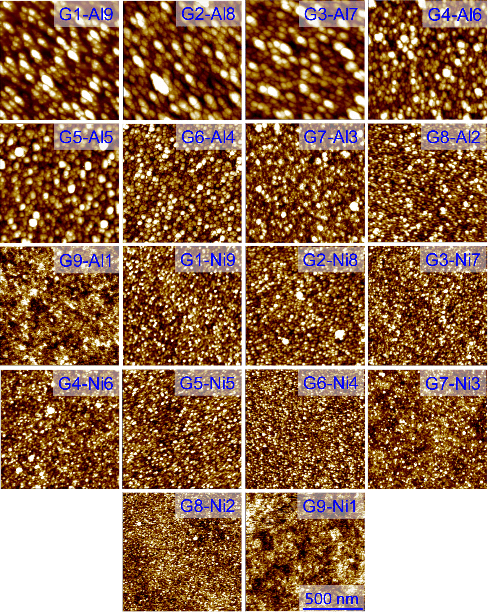 | ||
| Fig. 5 Surface topography (area: 1 × 1 μm) of the G:Al and G:Ni electrodes measured using AFM in noncontact mode. | ||
4. Conclusions
G:Al and G:Ni composites were deposited on a glass substrate using e-beam evaporation. The WF of the G:Al and G:Ni electrodes and their associated structural, optical, electrical, and morphological properties were investigated. The difference in the WF of the electrodes with different graphite content was examined. In calculating the WF, roughness was ignored because it was less than 10 nm. The WF for the G:Al and G:Ni electrodes could be tuned from 4.20 eV to 5.10 eV and from 4.67 eV to 5.10 eV, respectively, due to the formation of graphite–metal (Al/Ni) Ohmic contacts. The resistivity of the G1:Al9 and G1:Ni9 electrodes decreased from 352 Ω sq−1 to 2.284 ± 0.03 Ω sq−1 and from 4.903 ± 0.043 Ω sq−1, respectively. As the Al or Ni content increased, the reflectance increased. The reflectance of the graphite thin film was 28.04%, and that of the G1:Al9 and G1:Ni9 electrodes was 72.07% and 63.24%, respectively. As expected, the addition of metal NPs to a graphite composite film increased the optical reflectance. This proposed graphite–metal composite electrode can be utilized in photovoltaic applications that require a low cost, a high work function, and low-reflection anodes.
Funding
This study was supported by the National Research Foundation of Korea funded by the Korean government (No. 2016R1A3B1908249).Conflicts of interest
The authors declare no competing financial interests.References
- M. Seong, H. Kim, S. W. Lee, D. Kim and S. J. Oh, APL Mater., 2018, 6, 121105 CrossRef.
- C. Tian, A. Mei, S. Zhang, H. Tian, S. Liu, F. Qin, Y. Xiong, Y. Rong, Y. Hu and Y. Zhou, Nano Energy, 2018, 53, 160–167 CrossRef CAS.
- J. W. Kim and A. Kim, Curr. Appl. Phys., 2021, 31, 52–59 CrossRef.
- M. Xue, W. Wang, F. Wang, J. Ou, C. Li and W. Li, J. Alloys Compd., 2013, 577, 1–5 CrossRef CAS.
- B. H. Lee, I. H. Jung, H. Y. Woo, H. K. Shim, G. Kim and K. Lee, Adv. Funct. Mater., 2014, 24, 1100–1108 CrossRef CAS.
- D. B. Bert, A. Hadipour, M. M. Mandoc, T. Woudenbergh and P. W. Blom, Adv. Mater., 2005, 17, 621–625 CrossRef.
- I. Campbell, S. Rubin, T. Zawodzinski, J. Kress, R. Martin, D. Smith, N. Barashkov and J. Ferraris, Phys. Rev. B: Condens. Matter Mater. Phys., 1996, 54, R14321 CrossRef CAS PubMed.
- D. Cornil, Y. Olivier, V. Geskin and J. Cornil, Adv. Funct. Mater., 2007, 17, 1143–1148 CrossRef CAS.
- H. Lu, Z. Liu, X. Yan, D. Li, L. Parent and H. Tian, Sci. Rep., 2016, 6, 1 CrossRef PubMed.
- S. A. Sergiienko, D. M. Tobaldi, L. Lajaunie, D. V. Lopes, G. Constantinescu, A. L. Shaula and N. D. Shcherban, J. Mater. Chem. C, 2022, 10, 626–639 RSC.
- L. Gao, J. Souto-Casares, J. R. Chelikowsky and A. A. Demkov, J. Chem. Phys., 2017, 147, 214301 CrossRef PubMed.
- D. Wu, S. Wan, T. Zhai, J. Yang, R. Wang and S. Duhm, Phys. Status Solidi RRL, 2022, 16, 2100434 CrossRef CAS.
- A. V. Kesavan, B. R. Lee, K. R. Son, A. C. Khot, T. D. Dongale, V. Murugadoss, P. C. Ramamurthy and T. G. Kim, ACS Appl. Mater. Interfaces, 2021, 13, 4284 CrossRef CAS.
- D. S. Kang, S. M. Lee, S. H. Lee and J. S. Roh, Carbon Lett., 2018, 27, 108–111 Search PubMed.
- S. Krimm, J. Phys. Chem., 1953, 57, 22–25 CrossRef CAS.
- S. Krimm and A. V. Tobolsky, J. Polym. Sci., 1951, 7, 57–76 CrossRef CAS.
- M. Rashad, F. Pan, A. Tang and M. Asif, Prog. Nat. Sci.: Mater. Int., 2014, 24, 101 CrossRef CAS.
- A. Jabbar, G. Yasin, W. Q. Khan, M. Y. Anwar, R. M. Korai, M. N. Nizam and G. Muhyodin, RSC Adv., 2017, 7, 31100–31109 RSC.
- I. R. M. Kottegoda, N. H. Idris, L. Lu, J. Z. Wang and H. K. Liu, Electrochim. Acta, 2011, 56, 5815–5822 CrossRef CAS.
- J. Robertson, Philos. Mag. B, 1997, 76, 335–350 CrossRef CAS.
- A. Taylor, S. Baluchová, L. Fekete, L. Klimša, J. Kopeček, D. Šimek, M. Vondráček, L. Míka, J. Fischer, K. Schwarzová-Pecková and V. Mortet, Diamond Relat. Mater., 2022, 123, 108815 CrossRef CAS.
- V. V. Brus, M. I. Ilashchuk, I. G. Orletskyi, M. M. Solovan, G. P. Parkhomenko, I. S. Babichuk, N. Schopp, G. O. Andrushchak, A. I. Mostovyi and P. D. Maryanchuk, Nanotechnology, 2020, 31, 505706 CrossRef CAS PubMed.
- K. P. Maity and V. Prasad, Mater. Res. Express, 2019, 6, 0850a2 CrossRef CAS.
- M. Brohmann, F. J. Berger, M. Matthiesen, S. P. Schießl, S. Schneider and J. Zaumseil, ACS Nano, 2019, 13, 7323–7332 CrossRef CAS.
- C. Godet, Philos. Mag. B, 2001, 81, 205–222 CrossRef CAS.
- D. Dasgupta, F. Demichelis and A. Tagliaferro, Philos. Mag. B, 1991, 63, 1255–1266 CAS.
- N. F. Mott, Philos. Mag., 1969, 19, 835–852 CrossRef CAS.
- I. G. Austin and N. F. Mott, Adv. Phys., 1969, 18, 41 CrossRef CAS.
- M. Chen, W. Li, A. Kumar, G. Li, M. E. Itkis, B. M. Wong and E. Bekyarova, ACS Appl. Mater. Interfaces, 2019, 11, 19315–19323 CrossRef CAS PubMed.
- T. Brintlinger, M. S. Fuhrer, J. Melngailis, I. Utke, T. Bret, A. Perentes, P. Hoffmann, M. Abourida and P. Doppelt, J. Vac. Sci. Technol., 2005, 23, 3174–3177 CrossRef CAS.
- A. Datta, P. Becla and S. Motakef, Sci. Rep., 2019, 9, 1 CrossRef CAS PubMed.
- I. F. Patai and M. A. Pomerantz, J. Franklin Inst., 1951, 252, 239–260 CrossRef.
- K. H. Lee, W. K. Seong and R. S. Ruoff, Carbon, 2022, 187, 396–403 CrossRef CAS.
Footnote |
| † Electronic supplementary information (ESI) available. See DOI: https://doi.org/10.1039/d2tc02848d |
| This journal is © The Royal Society of Chemistry 2022 |