DOI:
10.1039/C8RA05211E
(Paper)
RSC Adv., 2018,
8, 29220-29227
Graphene based photoanode for DSSCs with high performances†
Received
18th June 2018
, Accepted 5th August 2018
First published on 16th August 2018
Abstract
Graphene assisted photoanodes are promising because of the high performance of the resulting dye sensitized solar cells (DSSCs). A photoanode with a three-layer structure is prepared in this study and the synergy between each layer was found to play a vital role in its photovoltaic properties. The influence of interface contact between the transport layer and work layer is revealed. After ameliorating the interface contact level (enhancing the electron transport ability), the functions of the adopted reduced graphene oxide (RGO) and three-dimensional graphene networks (3DGNs) in the transport layer and work layer, respectively, can be made full use of. In order to further enhance the scattering ability for the incident light and improve the adsorption ability for dye molecules, a scattering layer based on the RGO–TiO2 is added in the photoanode. After a comprehensive optimization (including the types of functional groups and mass fractions of the RGO in the work layer and scattering layer), the resulting power conversion efficiency reaches 11.8%, which is much higher than that of previous reported graphene modified DSSCs.
Introduction
Dye sensitized solar cells (DSSCs) have attracted increasing attention because of their non-toxic and low cost.1–6 Since the breakthrough energy conversion efficiency (η) achieved by Gratzel's group in 1991, related research on this topic has become very popular.7 In the past two decades, attention has been focused on fabricating more efficient dyes and finding better photoanode materials to further improve the resulting photovoltaic performance.8,9 Dye molecules act as the photon motor to realize photovoltaic conversion, which determines the incident photon to current conversion efficiency (IPCE) and exerts a significant impact on the resulting η.8 Gratzel et al. reported a series of dyes based on Ru complexes.10–12 Therein, N3 and N749 (called black dye) display high IPCE in a wide wavelength range, and the obtained η of the device exceeds 10%.10 Beside these high-cost Ru-based dyes, some new dyes including indoline, porphyrin and phthalocyanine have been fabricated in recent years.13–15 In fact, the corresponding properties of these reported dyes meet the requirements of DSSCs at this stage.
On the contrary, the bottleneck of DSSCs is the relatively low performance of the photoanode materials. Although nano-porous TiO2 (including ZnO) photoanode enhances the dye adsorption ability and introduces a relatively high η, the low fill factor (FF) restricts further improvement of the photovoltaic performances due to the high resistance.8 Some attempts have been carried out to avoid the extra loss of photo-induced electrons. Graphene, a strictly two-dimensional material, possesses unique properties such as an extremely high electron mobility (200![[thin space (1/6-em)]](https://www.rsc.org/images/entities/char_2009.gif) 000 cm2 V−1 s−1), a large theoretical BET area (2630 m2 g−1) and a high luminance efficiency (97% for a monolayer sample), which makes it a promising material for energy conversion devices.16,17 Shin's group reported a reduced graphene oxide (RGO) modified photoanode that achieved an enhancement of 20% for the η.18 Gao et al. adopted the RGO–TiO2 composite to prepare the photoanode and reported a remarkable increase in the photovoltaic performances.19 Considering the negative influence from the discontinuous construction of the RGO nanosheets on the electron transport, three-dimensional graphene networks (3DGNs) prepared by chemical vapor deposition method were used in the photoanode as fast electron transport channels by our group.20,21 Although the η increases to 9.1% (∼30% higher than that of the RGO added device), it is still far from the predicted value. After careful analysis, we found that the poor interface contact between the 3DGNs and TiO2 sets a barrier to the electron transport, leading to a remarkable loss of the photocurrent.21
000 cm2 V−1 s−1), a large theoretical BET area (2630 m2 g−1) and a high luminance efficiency (97% for a monolayer sample), which makes it a promising material for energy conversion devices.16,17 Shin's group reported a reduced graphene oxide (RGO) modified photoanode that achieved an enhancement of 20% for the η.18 Gao et al. adopted the RGO–TiO2 composite to prepare the photoanode and reported a remarkable increase in the photovoltaic performances.19 Considering the negative influence from the discontinuous construction of the RGO nanosheets on the electron transport, three-dimensional graphene networks (3DGNs) prepared by chemical vapor deposition method were used in the photoanode as fast electron transport channels by our group.20,21 Although the η increases to 9.1% (∼30% higher than that of the RGO added device), it is still far from the predicted value. After careful analysis, we found that the poor interface contact between the 3DGNs and TiO2 sets a barrier to the electron transport, leading to a remarkable loss of the photocurrent.21
As we know, the poor contact between the conductive substrate and photoanode brings about a high dark current, leading to a reduced short circuit current (JSC) and η.9,20 Recently, our group designed a series of photoanodes with a two-layer structure to depress the annihilation of photo-generated electrons and I3−¿¿ at the interface.9 A proper transport layer (prepared by the layer-by-layer assembly method) between the conductive substrate and work layer of the photoanode exerts a positive influence on the resulting photovoltaic performance.9 Moreover, we found that the reduction degree of the adopted RGO in the transport layer imposes a significant effect on the performance of the resulting functional layer.22 However, in some cases, we found that the added transport layer may not play an expected effect, indicating that some other factors influence the function of the transport layer.21 Based on our recent study, the interface condition between the graphene and TiO2 is found to exert a significant influence on the electron and phonon transport between them. The surface defect of the 3DGNs can act as the bridge to achieve ohmic contact between them.23–25 Therefore, we deem that the interface contact level between the transport layer and work layer may play a similarly vital role in the resulting η. Although the interface contact condition between the conductive substrate and transport layer is studied extensively,9,22 the interface contact level between the transport layer and work layer has never been revealed, which limits further improvement in graphene based-DSSCs. The optimization of the contact level between the transport layer and work layer to achieve synergy between them deserves more attention.
In this study, RGO and 3DGNs are used as modifiers to fabricate the transport layer and work layer of the photoanode. In order to improve the contact level between these two layers, some elaborate designs are adopted. Moreover, a scattering layer based on the RGO–TiO2 composite is prepared to improve the IPEC (increasing loading amount of dye). After optimizing the interface condition between the transport layer and work layer, a remarkable improvement in the photovoltaic performance of the resulting DSSCs is achieved, and a η value as high as 11.8% is obtained after further adding a scattering layer.
Results and discussion
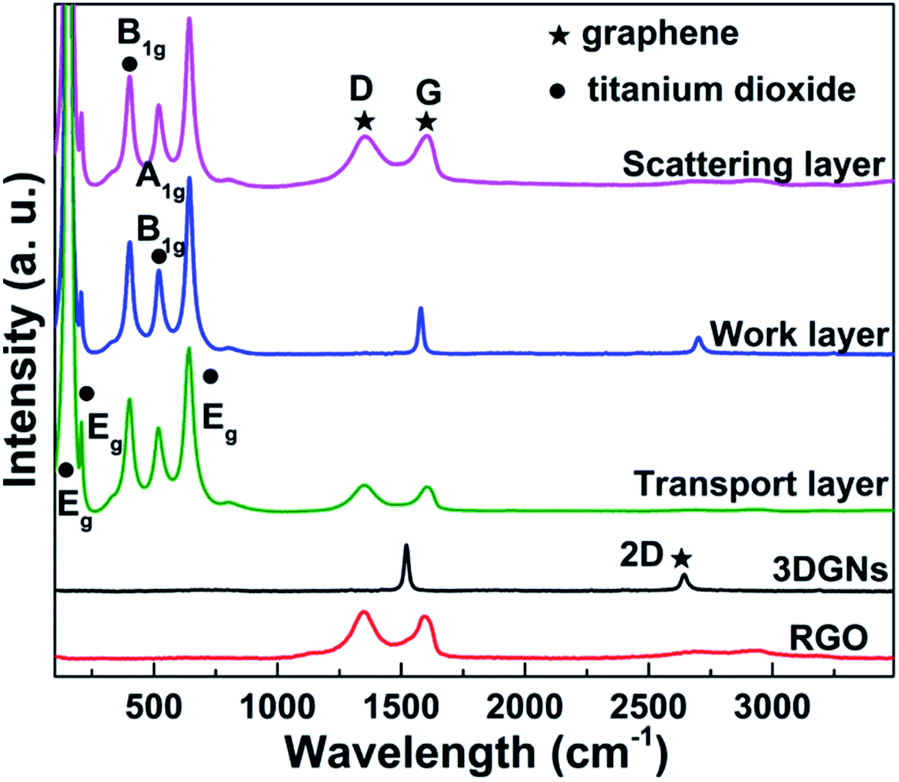
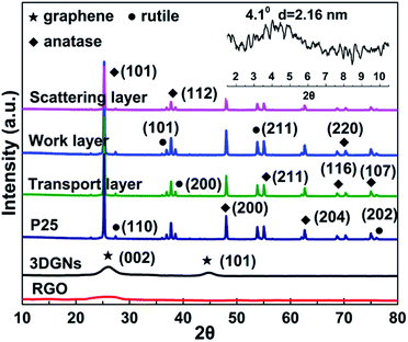
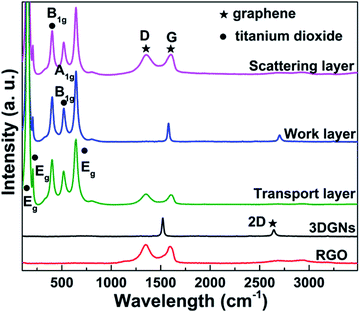
SEM images of the pristine nano TiO2, transport layer and work layer are shown in the Fig. 1. Average size of the pure TiO2 particles ranges from 20–30 nm (Fig. 1a), provides a pre-condition to achieve a uniform dispersion on the graphene surface. The transport layer (prepared by using the layer-by-layer assembly method, more details are supplied in the Experimental section) with the RGO terminal layer displays a much smoother surface compared with the case of the TiO2 terminal layer (Fig. 1b and c, the terminal layer is the finally deposited layer of the transport layer). Moreover, the lamellar structure of the alternative RGO and TiO2 layer can be seen by the cross-section image (Fig. 1d). As for the work layer, the 3DGNs not only act as the fast transport network for photo-induced electrons, but also as a scaffold to load TiO2 nanoparticles (Fig. 1e, the original 3DGNs is shown in the inset). After adding the RGO, no obvious difference other than some additional graphene nanosheets can be seen on the 3DGNs' surface (Fig. 1f, both the 3DGNs and RGO are marked). XRD patterns of the 3DGNs, RGO, TiO2 and resulting photoanode are displayed in Fig. 2. Compared with that of the 3DGNs, the characteristic peak corresponding to (101) (JCPDS card: 41-1487, which is closely related to the long-range order) disappears in the case of the RGO, indicating the discontinuous structure of the latter. Moreover, the signal located at 26.6° is assigned to the (002) lattice plane.26,27 As for the pure TiO2, both the characteristic peaks belonged to the anatase and rutile phases (JCPDS card: 84-1286 and JCPDS card: 21-1276) and can be seen in the profile. Moreover, the patterns of the resulting transport layer, work layer and scattering layer are almost identical.28 The phenomenon is reported in some previous works and the low mass fraction of the graphene indicates that the corresponding signal is drowned in the composites.29,30 Moreover, the periodic layered structure of the transport layer is confirmed by the small angle XRD profile and a peak located at 4.1° (which corresponds to layer spacing of 2.16 nm: the thickness of one RGO layer and one TiO2 layer) can be seen. Raman spectroscopy is a useful, non-destructive tool to obtain information such as thickness, quality and average size of the graphite-like materials, making it one of the most popular methods to analyze graphene samples.31–33 There are three major signals can be seen: G, D and 2D peaks. The G peak is associated with the E2g phonon at the Brillouin zone center and produces a signal at ∼1580 cm−1.31 The intensity and position of this peak is determined by the thickness and charge amount of the sample. D band is the fingerprint peak of the defective graphene (∼1350 cm−1), while the 2D peak is the second order signal of the D peak but free of defects.32 The intensity and position of the 2D peak can be used to identify the quality and thickness of graphene samples.33 The absence of the D peak from the profile of the 3DGNs implies its high quality (Fig. 3), which is further confirmed by the 2D peak (the intensity of 2D peak is much higher than that of the RGO sample). The major defects of the RGO are surface functional groups, and can be controlled by the reduction process (more details are provided in the ESI†). Moreover, the Raman signals induced by TiO2 in the low wavelength area belong to Eg, B1g and A1g modes.
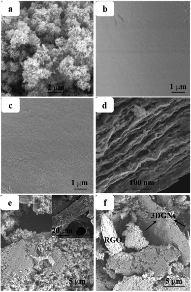 |
| | Fig. 1 SEM images of (a) TiO2 (b) transport layer with the RGO as the terminal layer (c) transport layer with the TiO2 as the terminal layer (d) cross-section view of the transport layer (e) the 3DGNs added work layer (the original 3DGNs shown in the inset) (f) the 3DGNs and RGO co-modified work layer. | |
 |
| | Fig. 2 XRD curves of the RGO, 3DGNs, TiO2, transport layer, work layer and scattering layer. The small angle XRD result of the transport layer is displayed as the inset. | |
 |
| | Fig. 3 Raman profiles of the RGO, 3DGNs, transport layer, work layer and scattering layer. | |
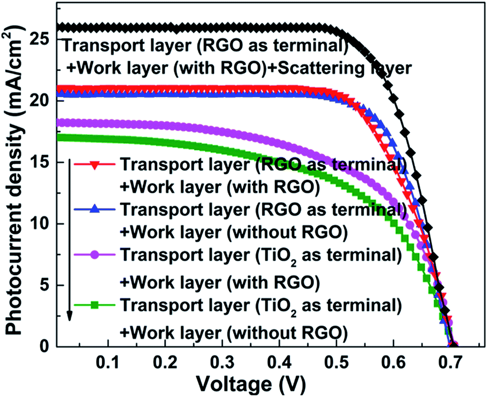
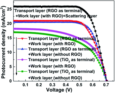
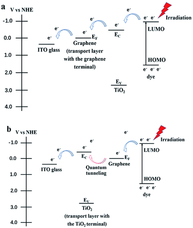
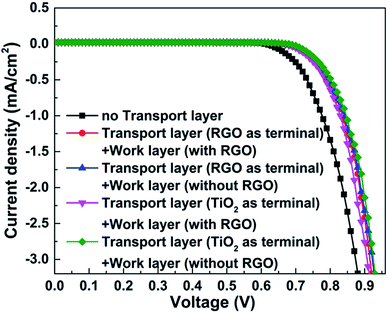
J–V curves of the resulting DSSCs with various photoanodes are recorded. As we can see from Fig. 4, the observed photovoltaic performances are deeply dependent on the structure of the adopted photoanode. Firstly, the function of the transport layer is closely related to its terminal layer. The transport layer displays an outstanding positive effect when the RGO is adopted as the terminal layer (both the JSC and η increase by ∼11% compared with the case when the transport layer is absent, Table 1), while no remarkable improvement can be found when TiO2 is used as the terminal layer. The transport process of photo-generated electrons in these two cases are described in the schematic diagrams of Fig. 5a and b (more details are supplied in the ESI†). The major distinguishing factor is the electron transport at the interface between the work layer and transport layer. Considering that the other conditions are identical, four possible reasons (including interface contact condition between the transport layer and work layer, interface contact condition between the transport layer and conductive substrate, change of the thickness of the work layer, change of the thickness of the transport layer) may lead to the observed distinction of the photovoltaic performance. The TiO2 terminal layer of the transport layer can be considered as a part of the work layer, which may induce the change of the photovoltaic performance because of the varying thickness of the work layer and transport layer. According to our previous study, the η increases from 4.96% to 6.25% when the thickness of the work layer changes from 10 to 15 μm.9 Similarly, the enhancement of η reaches ∼10% (from 6.99% to 7.68%) when the number of bi-layers in the transport layer increases from 50 to 200.21 However, the thickness of the TiO2 terminal layer in the transport layer is less than 2.16 nm (the thickness of one bi-layer structure), which is far from that of the work layer (the thickness of work layer is constant at ∼10 μm). Similarly, the change of thickness of the transport layer can be ignored because 200 bi-layers are adopted in the transport layer in this study. Therefore, the interface contact level is the major reason leading to the varying photovoltaic performances. The Fermi level of graphene is higher than the conduction band of TiO2, and the probability of electron transport from graphene to TiO2 is found to be less than 5 × 10⁻⁷ (quantum tunneling is found to be the sole path for achieving transport to overcome the Schottky barrier, ∼2 eV).27 Contrarily, an ohmic contact will form when the electrons are transported from TiO2 to graphene. Therefore, the electron transport (from TiO2 and 3DGNs to RGO) is more smooth when the RGO is adopted as the terminal layer compared with when a TiO2 terminal layer is adopted (electron transport from 3DGNs and TiO2 to TiO2). In order to confirm this point of view, the photocurrent of these photoanodes were measured. As expected, the photocurrent from the photoanode that possessed a better interface contact (reducing electron loss at the interface area) between the work layer and transport layer was ∼18% higher than that in another case (Fig. 6). Considering the BET area (which influences the loading amount of dye, ∼270 m2 g−1) and illumination condition are identical, the observed distinctions result from two possible reasons: (1) interface contact between the work layer and transport layer and (2) interface contact between the transport layer and conductive substrate. The latter determines the dark current of the device which were recorded (Fig. 7). As shown in the patterns, the dark currents of the photoanodes which possess a transport layer are much lower than that of the pure TiO2 photoanode. Moreover, similar dark currents of various photoanodes with different transport layers indicate that the electron loss at the interface of photoanode and conductive substrate has nothing to do with the specific terminal layer of the transport layer. Therefore, the interface contact level between the transport layer and work layer imposes a significant influence on the resulting photovoltaic performances. The type of terminal layer has a vital role in the determination of the resulting properties and explains the discrepancy from previous reports.9,21
 |
| | Fig. 4
J–V curves of DSSCs with various photoanodes. | |
Table 1 Photovoltaic performances of devices with various photoanodes
| Photoanodes |
Parameters |
Loading dye (×10−7 mol cm−2) |
|
J
SC (mA cm−2) |
V
oc (mV) |
FF (%) |
η (%) |
| 3DGNs added work layer |
16.8 |
703 |
0.61 |
7.20 |
1.36 |
| Transport layer (TiO2 terminal) + 3DGNs added work layer |
17.0 |
705 |
0.61 |
7.31 |
1.37 |
| Transport layer (RGO terminal) + 3DGNs added work layer |
18.2 |
708 |
0.62 |
7.99 |
1.31 |
| Transport layer (TiO2 terminal) + 3DGNs and RGO added work layer |
20.6 |
706 |
0.62 |
9.02 |
1.42 |
| Transport layer (RGO terminal) + 3DGNs and RGO added work layer |
21.1 |
702 |
0.65 |
9.63 |
1.38 |
| Transport layer (RGO terminal) + 3DGNs and RGO added work layer + scattering layer |
26.0 |
709 |
0.64 |
11.80 |
1.77 |
 |
| | Fig. 5 Schematic diagrams of electron transport in the photoanode (a) the transport layer with the RGO as the terminal layer (b) the transport layer with the TiO2 as the terminal layer. | |
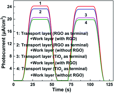 |
| | Fig. 6 Photocurrents of various photoanodes. | |
 |
| | Fig. 7 Dark currents of devices with various photoanodes. | |
Moreover, the observed photovoltaic performances from J–V curves show that the presence of the RGO in the work layer has a positive influence on the devices. Our group has proven that the interface contact level between the graphene basal plane and TiO2 nano-particles in the work layer is quite important to the resulting photovoltaic performances.20,21 Therein, the surface functional groups of the RGO act as the linker to improve the interface contact level. Similarly, the RGO modifier in the work layer provides a better interface contact condition for electron transport from the work layer to transport layer. The photocurrents of photoanodes are shown in Fig. 6 and shows obvious disparities, thus proving the ameliorative contact level between the transport layer and work layer after adding the RGO in the work layer. Besides ameliorating the electron transport ability at the interface area, the added RGO exerts a positive influence on the electron transport in the work layer. According to the obtained results (Table 1), the enhancement of the η is about 20% after adding 4 wt% RGO into the work layer. As we know, the major aim of adding graphene into the work layer is improving its electron transport ability and ameliorating the electron transport level at the interface area, and some groups have made relative studies. In the first phase, the RGO is widely adopted as the modifier.19,34,35 However, some researchers found that the obtained enhancement is far from the expected value due to the high defect density and discontinuous structure of the RGO.36,37 Contrarily, the high quality and continuous structure endows the 3DGNs (prepared by chemical vapor deposition method) with a more promising modifier, which has been proven by Yen's group, Huang's group and our group.20–22,38,39 With the identical mass fraction (1 wt%), the η increases from 5.86% to 6.56% when the RGO is replaced by the 3DGNs. Therefore, the 3DGNs rather than RGO possesses better electron transport ability when used as the modifier for the work layer. However, even when the added RGO is replaced by the 3DGNs in this study, the obtained η (9.14%) is lower than that of the 3DGNs and RGO co-modified device (9.63%). Therefore, the major function of the added RGO in the work layer is ameliorating the electron transport level at the interface between the transport layer and work layer in this study.
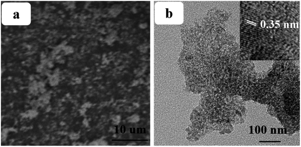
Beside the electron transport ability, the resulting photovoltaic performances are strongly dependent on the scattering ability (for incident light) and adsorption ability (for dye) of the employed photoanode. The relationship between the average size of particles of the photoanode and wavelength of the incident light is the paramount factor influencing the scattering ability of the photoanode and a remarkable increase will be achieved when these two values are comparable. Considering that the size of particles in the work layer is small (TiO2 nanoparticles 20–30 nm), the scattering ability for visible-light (400–760 nm) is weak, restricting the absorption efficiency of incident photons as well as the IPEC (Fig. 8). Therefore, designing a functional layer to enhance the scattering ability for visible-light is meaningful. Moreover, the scattering layer should possess good compatibility (simultaneously including good interface contact conditions between the work layer and dyes) with the device. According to our previous study, the average size of the RGO–TiO2 composite, which is fully compatible with the work layer and dyes, can be controlled by adjusting the reaction conditions during the hydrothermal procedure.28 SEM and TEM images of the scattering layer is shown in the Fig. 9 with the graphene sheets and TiO2 particles marked. By adjusting the reaction conditions, the average size of the composite is adjusted to ∼600 nm (Fig. 9b), achieving an enhanced scattering ability for the incident visible-light. The (101) lattice plane of the TiO2 particles can be identified by the lattice spacing in the inset. With a decrease in reaction time, the agglomeration of the composite decreases (more details are provided in the ESI†).
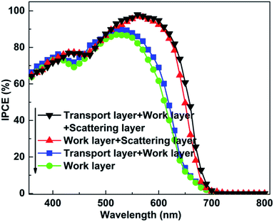 |
| | Fig. 8 IPCE patterns of devices with various photoanodes. | |
 |
| | Fig. 9 SEM (a) and TEM (b) images of the RGO–TiO2 scattering layer, the high magnificent image of the material is shown in the inset. | |
After adding the RGO–TiO2 scattering layer onto the work layer, the corresponding IPEC and photovoltaic performances are enhanced significantly (Fig. 6 and 8). A ∼10% increase can be seen for the IPEC in the long wavelength range, indicating the significance of employing the scattering layer. Moreover, the JSC increases to 24.6 mA cm−2 at the same time, proving the yield of photo-induced electrons grows remarkably even when the irradiation condition is unvaried. Besides the scattering ability for the incident light, the adsorption ability of dye molecules, which is closely related to its BET area, is crucial to the resulting property of the photoanode. The large BET area of graphene is another reason to add a promising modifier for the scattering layer (586 m2 g−1 for the scattering layer). Therefore, the RGO–TiO2 is a satisfactory composite for the scattering layer (loading amount of dye enhances remarkably after adding the scattering layer, Table 1).
Recently, the contact levels between the RGO and other materials (including inorganic matters and organic matters) were revealed by our group where the total amount and types of the functional groups on the RGO surface were found to be acting as the determinants.40–42 After optimizing these two parameters, the Celement:Chydroxyl:Cepoxy:Ccarboxyl = 63:16:3:18 and Celement:Cfunction = 1.7:1 are recommended for adoption as the modifier for the photoanode (the corresponding XPS curves and detailed preparation process are provided in the ESI†), and the resulting JSC and η increase to 26.0 mA cm−2 and 11.8% (∼6% higher than the case without the optimization process). Moreover, a synergy between the mass fraction of the RGO in the work layer (as well as in the scattering layer) and the resulting photovoltaic performance is discovered. The 4 wt% and 5 wt% RGO in the work layer and scattering layer achieve the best photovoltaic performances. A lower mass fraction of the RGO cannot completely ameliorate the interface contact condition between the transport layer and work layer, while the function of the excess RGO can be ignored because the total amount of the photo-generated electrons is limited.
Experimental
Materials
P25 was purchased from Degussa. Acetonitrile, polytetrafluoroethylene and sodium dodecyl sulfate were purchased from the Beijing chemical reagent plant (Beijing, China). Chloroplatinic acid, natural graphite, indoline, polyethyleneimine (PEI) aqueous solution, iodine and potassium iodide were obtained commercially from Aladdin Co. Deionized water was utilized to prepare all aqueous solutions. The P25 sample was sintered at 350 °C for 4 h to remove the organics and dust for the subsequent experiments.
Preparation
Preparation of the 3DGNs, RGO, TiO2 nanosheets, graphene–TiO2 transport layer, pure TiO2 photoanode, 3DGNs–TiO2 photoanode and Pt electrode have been reported by us previously.8,20–22 The transport layer was fabricated by the layer-by-layer assembly technology. Briefly, a conductive glass substrate was immersed into the protonic PEI aqueous solution for 15 min to introduce positive charges and then washed twice with deionized water (step 1). After that, the conductive glass was immersed into the TiO2 nanosheet solution for 15 min and then washed twice (step 2). Then, the sample was immersed into the PEI solution for 15 min and rinsed twice (step 3). Lastly, the substrate was immersed into the RGO solution for 15 min and washed twice (step 4). These steps were repeated until the desired number of bi-layers (a 200 bi-layer structure is adopted in this study) were obtained (the TiO2 or RGO can be designed as the terminal layer when step 2 or step 4 is performed as the last step. The terminal layer is the finally deposited layer). Subsequently, the prepared films were illuminated under UV-light for 24 h to remove the PEI. The RGO and 3DGNs co-modified TiO2 work layer was prepared as follows: the 3DGNs (2 wt%) and RGO nanosheets (2–8 wt%) were mixed with TiO2 nanoparticles and moved into an ethanol solution for the supersonic treatment (50 min). Then, the resulting paste was deposited on a conductive glass (or transport layer) by the doctor-blade approach. The scattering layer is fabricated by the hydrothermal method. Briefly, a certain amount of RGO (1–10 wt%) and P25 were added into the sodium hydroxide solution with an ultrasonic treatment (4 h) and the mixture was transferred into a reactor maintained at a specific temperature (150–220 °C) for a certain time (12–24 h). After the reaction, the composite was dried at 90 °C for 12 h and then put into the alcohol solution and stirred for 40 min to form a paste. The resulting paste was deposited on the work layer to act as the scattering layer. The thicknesses of all the work layers and scattering layers are 10 μm and 5 μm, respectively.
Characterization
X-ray photoelectron spectroscopy (XPS) was measured on an RBD upgraded PHI-5000C ESCA system (Perkin Elmer). The morphology images were obtained by scanning electron microscope (SEM) (FEI Sirion 200 scanning electron microscope) and transmission electron microscopy (TEM) (JEM-2100F). X-ray diffraction (XRD) patterns were recorded on a Bruker D8 Advance (Cu Kα radiation 0.154 nm). Raman spectra were recorded by a LabRam-1B Raman microspectrometer at 514.5 nm (Horiba Jobin Yvon, France). The BET surface areas were measured on a Nova 100 by using N2 as the adsorption gas. Photocurrent measurements were performed on a CHI 660D electrochemical analyzer (Shanghai CH Instrument Company, China). The J–V curves were recorded by a PGSTAT 30 potentiostat (Netherlands). The incident photon-to-current conversion efficiency (IPCE) profiles were recorded on a Newport 1918-c power meter. The loading amount of the indoline was calculated by the concentration difference of the dye in the solution before and after adsorption by the photoanode (adsorption time is 24 h). The concentration of dye in the solution is proportional to the integral area of the adsorption peak measured by the UV-visible spectrometer (the adsorption signal was located at ∼510 nm).43,44
Conclusions
Graphene based photoanodes were prepared and adopted to modify the DSSCs and the resulting photovoltaic performances were found to be closely related to the structure of the fabricated photoanodes. Firstly, the terminal layer of the transport layer determines the interface contact level between the transport layer and work layer. Similarly, the presence of RGO in the work layer further ameliorates the interface condition. Based on the obtained photovoltaic performances, the interface contact condition exerts a remarkable influence on the JSC, FF and η, which is similar to the effect from the interface condition between the transport layer and conductive substrate. The scale of photocurrent and dark current prove this point of view. Moreover, a scattering layer based on the RGO–TiO2 composite was fabricated to enhance the scattering ability for incident light and to increase the BET area for a higher dye loading amount. After optimizing the structures of the transport layer, work layer and scattering layer, the resulting η reaches 11.8%, which is much higher than that of the previously reported graphene based-DSSCs.
Conflicts of interest
There are no conflicts to declare.
Acknowledgements
This work is supported by National Natural Science Foundation of China (51506012, 51671037, 51706023), Natural Science Foundation of Jiangsu Province (BK20150266), Special Foundation of Sci-Tech achievements transformation of Jiangsu province (BA2015166).
Notes and references
- E. Singh, K. S. Kim, G. Y. Yeom and H. S. Nalwa, RSC Adv., 2017, 7, 28234–28290 RSC.
- D. T. Wang, W. X. Wang, X. Y. Ma, C. Zhang, J. S. Zhao and X. X. Zhang, Ind. Eng. Chem. Res., 2015, 54, 12639–12645 CrossRef CAS.
- A. Ashok, S. N. Vijayaraghavan, S. V. Nair and M. Shanmugam, RSC Adv., 2017, 7, 48853–48860 RSC.
- S. L. Li, H. H. Min, F. Xu, L. Tong, J. Chen, C. Y. Zhu and L. T. Sun, RSC Adv., 2016, 6, 34546–34552 RSC.
- J. C. Kim, M. M. Rahman, M. J. Ju and J. J. Lee, RSC Adv., 2018, 8, 19058–19066 RSC.
- S. Venkatesan, E. S. Darlim, M. H. Tsai, H. Teng and Y. L. Lee, ACS Appl. Mater. Interfaces, 2018, 10, 10955–10964 CrossRef CAS.
- B. Oregan and M. Gratzel, Nature, 1991, 353, 737–740 CrossRef CAS.
- C. Y. Lin, Y. H. Lai, H. W. Chen, J. G. Chen, C. W. Kung and R. Vittal, Energy Environ. Sci., 2011, 4, 3448–3455 RSC.
- B. Tang and G. X. Hu, J. Power Sources, 2012, 220, 95–102 CrossRef CAS.
- W. Xu, J. Pei, J. F. Shi, S. J. Peng and J. Chen, J. Power Sources, 2002, 183, 792–798 CrossRef.
- M. K. Nazeeruddin, P. Pechy and M. Gratzel, Chem. Commun., 1997, 33, 1705–1706 RSC.
- J. Rochford, D. Chu and A. Hagfeldt, J. Am. Chem. Soc., 2007, 129, 4655–4665 CrossRef CAS.
- M. K. Nazeeruddin, P. Pechy, T. Renouard, S. M. Zakeeruddin, R. H. Baker and M. Gratzel, J. Am. Chem. Soc., 2001, 123, 1613–1624 CrossRef CAS.
- T. Horiuchi, H. Miura and S. Uchida, Chem. Commun., 2003, 39, 3036–3037 RSC.
- G. D. Sharma, P. Suresh, M. S. Roy and J. A. Mikroyannidis, J. Power Sources, 2010, 195, 3011–3016 CrossRef CAS.
- B. Tang and G. X. Hu, Chem. Vap. Deposition, 2014, 20, 14–22 CrossRef CAS.
- B. Tang, G. X. Hu and H. Y. Gao, Int. J. Heat Mass Transfer, 2015, 85, 420–429 CrossRef CAS.
- Y. E. Shin, Y. J. Sa and S. Park, Nanoscale, 2014, 6, 9734–9741 RSC.
- S. R. Sun, L. Gao and Y. Q. Liu, Appl. Phys. Lett., 2010, 96, 083113–083115 CrossRef.
- B. Tang and G. X. Hu, J. Power Sources, 2013, 234, 60–68 CrossRef CAS.
- B. Tang, G. J. Ji, Z. W. Wang, H. Q. Chen, X. F. Li, H. G. Yu, S. Li and H. Liu, RSC Adv., 2017, 7, 45280–45286 RSC.
- Y. F. Sun, Y. C. Cao, W. Q. Huang, Y. J. Zhu, L. Heng and B. Tang, Mater. Lett., 2016, 165, 178–180 CrossRef CAS.
- B. Tang, H. Q. Chen, Y. F. He and Z. W. Wang, Compos. Sci. Technol., 2017, 150, 54–64 CrossRef CAS.
- B. Tang, S. L. Wang, J. Zhang, Z. W. Wang, Y. F. He and W. Q. Huang, Int. Mater. Rev., 2018, 63, 204–225 CrossRef CAS.
- B. Tang, H. Q. Chen, H. P. Peng, Z. W. Wang and W. Q. Huang, Nanomaterials, 2018, 8, 105–131 CrossRef.
- H. S. Song, C. H. Ko, W. Ahn, B. J. Kim, E. Croiset, Z. W. Chen and S. C. Nam, Ind. Eng. Chem. Res., 2012, 51, 10259–10264 CrossRef CAS.
- G. X. Hu and B. Tang, Mater. Chem. Phys., 2013, 138, 608–614 CrossRef CAS.
- M. Akizuki and Y. Oshima, Ind. Eng. Chem. Res., 2017, 56, 6204–6212 CrossRef CAS.
- X. Y. Zhang, H. P. Li, X. L. Cui and Y. H. Lin, J. Mater. Chem., 2010, 20, 2801–2806 RSC.
- H. Zhang, X. J. Lv, Y. M. Li, Y. Wang and J. H. Li, ACS Nano, 2010, 4, 380–386 CrossRef CAS.
- B. Tang, G. X. Hu and H. Y. Gao, Appl. Spectrosc. Rev., 2010, 45, 369–407 CrossRef CAS.
- A. C. Ferrari, J. C. Meyer, V. Scardaci, C. Casiraghi, K. S. Novoselov and A. K. Geim, Phys. Rev. Lett., 2006, 97, 187401–197404 CrossRef CAS.
- M. Sarno, G. Rossi, C. Cirillo and L. Incarnato, Ind. Eng. Chem. Res., 2018, 57, 4895–4906 CrossRef CAS.
- X. Wang, L. Zhi and K. Mullen, Nano Lett., 2008, 8, 323–327 CrossRef CAS.
- T. H. Tsai, S. C. Chiou and S. M. Chen, Int. J. Electrochem. Sci., 2011, 6, 3333–3343 CAS.
- Z. P. Chen, W. C. Ren, L. B. Liu, S. F. Pei and H. M. Chen, Nat. Mater., 2011, 10, 424–428 CrossRef CAS.
- D. R. Dreyer, S. J. Park, W. C. Bielawski and R. S. Ruoff, Chem. Soc. Rev., 2010, 39, 228–240 RSC.
- M. Y. Yen, M. C. Hsiao and S. H. Liao, Carbon, 2011, 49, 3597–3606 CrossRef CAS.
- J. Zhi, H. L. Cui, A. Chen and F. Q. Huang, J. Power Sources, 2015, 281, 404–410 CrossRef CAS.
- J. Zhang, S. Li, B. Tang, Z. W. Wang, G. J. Ji, W. Q. Huang and J. P. Wang, Nanoscale Res. Lett., 2017, 12, 457–461 CrossRef.
- Y. F. Sun, Y. F. He, B. Tang, C. B. Tao, J. M. Ban and L. Jiang, RSC Adv., 2017, 7, 55790–55795 RSC.
- B. Tang, Z. W. Wang, W. Q. Huang, S. Li, T. T. Ma, H. G. Yu and X. F. Li, Nanoscale Res. Lett., 2017, 12, 527–533 CrossRef.
- M. Matsui, R. Aoki, D. Nishiwaki, Y. Kubota, K. Funabiki, J. Jin, T. Yoshida, S. Higashijima and H. Miura, RSC Adv., 2015, 5, 57721–57724 RSC.
- Y. Z. Li, Y. C. Li, P. Song, F. C. Ma, J. P. Liang and M. T. Sun, RSC Adv., 2017, 7, 20520–20536 RSC.
Footnote |
| † Electronic supplementary information (ESI) available. See DOI: 10.1039/c8ra05211e |
|
| This journal is © The Royal Society of Chemistry 2018 |
Click here to see how this site uses Cookies. View our privacy policy here. 
 Open Access Article
 This Open Access Article is licensed under a Creative Commons Attribution-Non Commercial 3.0 Unported Licence
 *,
Haogang
Yu
,
Haoping
Peng
,
Zhengwei
Wang
,
Sen
Li
,
Tingting
Ma
and
Weiqiu
Huang
*,
Haogang
Yu
,
Haoping
Peng
,
Zhengwei
Wang
,
Sen
Li
,
Tingting
Ma
and
Weiqiu
Huang