
 Open Access Article
 This Open Access Article is licensed under a Creative Commons Attribution-Non Commercial 3.0 Unported Licence
The lab-on-PCB approach: tackling the μTAS commercial upscaling bottleneck
Despina
Moschou
 *a and
Angeliki
Tserepi
b
*a and
Angeliki
Tserepi
b
aCentre for Advanced Sensor Technologies, Department of Electronic and Electrical Engineering, University of Bath, BA2 7AY, Bath, UK. E-mail: d.moschou@bath.ac.uk
bInstitute of Nanoscience and Nanotechnology, National Center for Scientific Research “Demokritos”, Patriarchou Gregoriou and 27 Neapoleos Str., 153 41 Aghia Paraskevi, Attiki, Greece. E-mail: a.tserepi@inn.demokritos.gr
First published on 6th March 2017
Abstract
Commercialization of lab-on-a-chip devices is currently the “holy grail” within the μTAS research community. While a wide variety of highly sophisticated chips which could potentially revolutionize healthcare, biology, chemistry and all related disciplines are increasingly being demonstrated, very few chips are or can be adopted by the market and reach the end-users. The major inhibition factor lies in the lack of an established commercial manufacturing technology. The lab-on-printed circuit board (lab-on-PCB) approach, while suggested many years ago, only recently has re-emerged as a very strong candidate, owing to its inherent upscaling potential: the PCB industry is well established all around the world, with standardized fabrication facilities and processes, but commercially exploited currently only for electronics. Owing to these characteristics, complex μTASs integrating microfluidics, sensors, and electronics on the same PCB platform can easily be upscaled, provided more processes and prototypes adapted to the PCB industry are proposed. In this article, we will be reviewing for the first time the PCB-based prototypes presented in the literature to date, highlighting the upscaling potential of this technology. The authors believe that further evolution of this technology has the potential to become a much sought-after standardized industrial fabrication technology for low-cost μTASs, which could in turn trigger the projected exponential market growth of μTASs, in a fashion analogous to the revolution of Si microchips via the CMOS industry establishment.
 Despina Moschou | Dr. Despina Moschou (M. Eng. Electrical and Computer Engineering, PhD in Microelectronic Technology) is a 50th anniversary Prize Fellow in Bioelectronics, within the Department of Electronic & Electrical Engineering at the University of Bath. Since 2010, her main research focus has been in the development of disposable lab-on-a-chip systems for bioanalytical applications (molecular and immunoassay-based point-of-care diagnostic devices). For the past 6 years, she has been pursuing the lab-on-printed circuit board approach, in an effort to realize disposable, mass-manufacturable lab-on-a-chip microsystems. Her interests also include inkjet printing technologies, adding further functionality to biomedical diagnostic systems. |
 Angeliki Tserepi | Dr. Angeliki Tserepi is Director of Research at the Institute of Nanoscience and Nanotechnology, National Center for Scientific Research “Demokritos”, Athens, Greece. She received a PhD in Chemical Physics from Ohio State University, USA, in 1994, and a European “Marie Curie” post-doctoral Fellowship at the Université Joseph Fourier, Grenoble, France (1994–1996). Her current research focuses on plasma-enabled surface engineering for control of wettability, biomolecule immobilization and cell attachment, and its implementation in microfluidic and lab-on-a-chip devices for food safety and medical diagnostics, where the PCB-based approach emerges as a very promising manufacturing technology. |
1 Introduction
Since the introduction of the micro total analysis system (μTAS) concept,1 the global excitement for this revolutionary technology has been exponentially increasing,2 owing to its tantalizing advantages over conventional laboratory tests:3 rapid response time, miniaturized sample volumes, automation, portability and reduced cost. The extensive research efforts from the increasingly growing global lab-on-a-chip (LoC) community over these years have proven these advantages and the feasibility of having such devices in real-life use. Based on such highly promising proof-of-concept devices, LoC research has benefitted from substantial investment, both from public funding bodies and from private investment. Despite all of these factors, clearly indicating that a LoC revolution is bound to happen soon, very few LoC-based diagnostic tests have been successfully commercialized3 until now, achieving real-life adoption.The reasons accounting for this discrepancy have been identified by researchers over the past few years and present the topical challenges for the LoC community; in one sentence, LoCs must become better suited for real world analyses. What does this come down to?4,5
a) Sample to answer microchips, implying a high degree of integration (sample preparation, reagent manipulation, biochemical reactions, and quantitative detection modules on a single platform);
b) cost-effective mass-manufacturing;
c) LoC design standardization, similar to electronics;
d) user-friendly LoC interfacing with the macroscopic world.
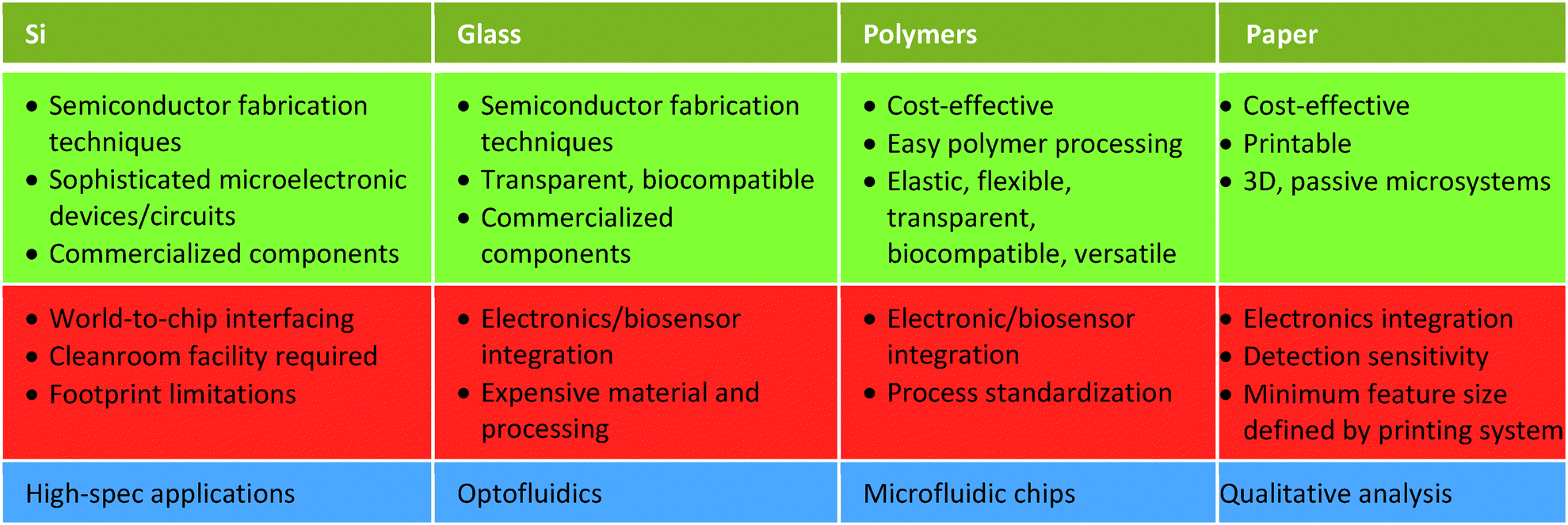
Several fabrication technologies have been explored until now; however, the currently prevailing approaches (Si, glass, polymers, paper)6 have not been able to address these points convincingly. In this review, we aim to analyze such technologies, in the light of their commercialization potential, while showcasing the upscaling advantages of a recently re-emerging technology: lab-on-PCB (lab-on-printed circuit board).
The idea of exploiting PCBs as a platform for integrated fluidic/electronic microsystems was first proposed in the late 1990s;7,8 however, alternative technologies (CMOS, polymers) dominated the LoC research arena; the focus of the LoC community at that point in time was mainly on demonstrating LoC component proof-of-concept microchips, and not particularly on integration strategies and micromanufacturing. Nowadays, with low-cost upscaling of highly integrated LoCs being a technology driver, the lab-on-PCB9 approach presents a promising alternative. While the academic publications are currently dominated by alternative strategies, the exponential trend (Fig. 1) in archived PCB based LoC publications is indicative of its future potential. In this review, we will present reported lab-on-PCB components and microsystems and the recent developments in the field, along with this technology's upscaling advantages and commercialization potential, supported by the European Institute of Printed Circuits (EIPC).
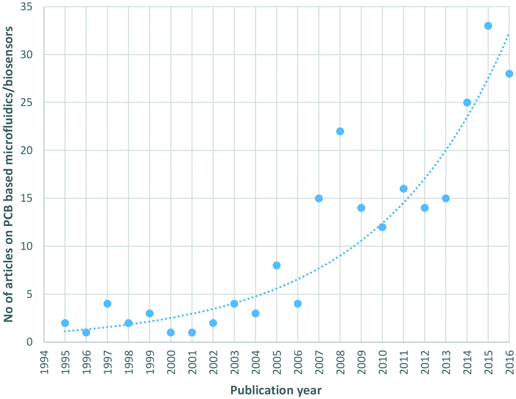 | ||
| Fig. 1 Number of published articles on PCB-based sensors and LoCs over the past 20 years (Scopus search, 12/11/2016, keywords: “printed circuit board” + “microfluidics” and “printed circuit board” + “biosensor”). | ||
2 Past and current μTAS high-volume production strategies
The standardization of integrated circuit (IC) microfabrication led the development of early microfluidic and microelectromechanical systems,10 even before the concept of μTAS was proposed by Manz et al.,1 owing to the maturity of clean room-based techniques. Features on the micrometer scale could be achieved consistently and reliably, adapting already available processing techniques. Since the most widely used substrate in microfabrication is the Si wafer, the first prototypes were Si-based; nonetheless, glass is a substrate that is also clean room-compatible and at the same time optically transparent and chemically inert.11 These advantages led to the commercialization of glass microfluidics over Si ones. However, clean room-based processing for relatively large footprint MEMs faces significant cost-limitations; therefore, microfluidics researchers and industries currently focus on lower cost materials, such as polymers and paper. All of the aforementioned materials and accompanying manufacturing approaches feature specific competitive advantages and disadvantages that have been presented in numerous review articles. For reasons of completeness, they will be briefly presented in the following sections, demonstrating each material suitable for specific applications.2.1 Si and glass technologies
Silicon has dominated the CMOS IC industry for the past decades, owing to its manufacturability in commercial clean room facilities. Clean room microfabrication consists of many standard processes:111. nanometer-scale patterning (photolithography, e-beam lithography, etc.);
2. additive processes (physical and chemical vapor deposition, sputtering, spin-coating, etc.);
3. micromachining (wet/dry etching, lift-off, diamond scribing, laser micromachining, etc.);
4. chip bonding (anodic bonding, adhesive bonding, fusion bonding, etc.);
Sophisticated biosensors and μTAS components12–16 have been developed over the past decades in silicon17 (Fig. 2A), innovatively combining such techniques and achieving impressive performance. Currently, there are several manufacturers offering Si microfluidics, positioned as fabs for μTAS designers (LioniX,18 Micralyne19).
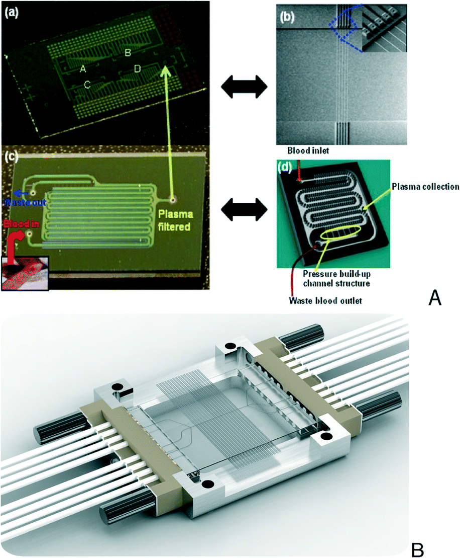 | ||
| Fig. 2 A) Si nanowire biosensing platform (a and b) and integrated plasma filtration microfluidic (c and d) for cardiac biomarker quantification (reprinted from ref. 17, copyright 2011, with permission from Elsevier) and B) glass microfluidic interfacing (Dolomite Ltd.).32 | ||
Due to CMOS processing inherent compatibility with microelectronic components (transistors, signal processing circuitry), the most sensitive and specific biosensors currently available have been first obtained with this technology. Based on the miniaturization advantage that has driven the semiconductor industry in the past decades, stand-alone silicon chips can be produced in mass volumes, at a very low cost; the more chips that fit within a Si wafer, the lower the overall processing cost.
However, this inherent advantage becomes a disadvantage for applications such as complete sample-in-answer-out LoCs: the chips are just too small to be interfaced with the macroscopic world (and thus the end-users) in a practical way. In order to overcome this obstacle, one would have to increase the footprint of the final device, decreasing the number of produced chips per wafer and thus increasing dramatically the cost of the final product. Clean room processing can indeed achieve optimum performance devices but can prove extremely expensive and laborious compared to other options, therefore it should be ideally employed in μTAS applications where increased sensitivity and accuracy requirements are more important than the actual cost of the LoC device20 (i.e. clinical laboratory equipment, next generation sequencing, nanofluidics, etc.), exploiting the unique advantages of Si (high chemical resistance, mechanical strength, temperature stability, high aspect ratio or high accuracy on large footprints).
Building on these Si characteristics, hybrid approaches have been followed by researchers so as to combine miniaturized Si chips with other, lower-cost materials like polymers,21 in order to achieve more efficient world-to-chip interfacing. Nonetheless, these hybrid approaches require custom bonding techniques20 from each manufacturer to ensure fluidic sealing between the different materials and thus would not allow cost-effective standardized commercial upscaling yet.
Glass substrates22 (Fig. 2B) are also used as a standard in clean room processing, combining the advantages of Si with optical transparency (requirement for optical detection LoC systems), biocompatibility, low non-specific adsorption, dielectric properties and gas impermeability. Therefore, for many years, glass has been considered the substrate of choice,5,23–25 with sophisticated μTASs demonstrated by research groups globally.26–30 It allowed the commercialization of several microfluidic components (Micronit,31 Dolomite,32 Caliper-currently Perkin Elmer33). Standard interfacing solutions34 (Fig. 2B) for such glass LoCs are currently available from manufacturers (IDEX,35 Dolomite,36 Micronit37). So why haven't we seen a wider adoption of glass LoCs? Indicatively, the current cost of a simple glass microfluidic mixer (4.5 × 1.5 cm2) lies in the order of hundreds of dollars. In addition, the hardness of glass poses limits to its broad application in microfluidics, with its gas impermeability not allowing its use for long-term cell culturing applications. Therefore, glass microchips are ideally suited for high-end applications (Table 1) that can accommodate high costs, employing mainly electroosmotic mobility and optical detection approaches.22
|
2.2 Polymer technologies
The limitations of Si and glass substrates, as mentioned above, motivated the development of other chip materials that can be easily fabricated and are compatible with a broad spectrum of biological applications. Generally speaking, an inherent property of microfluidic devices is their increased surface to volume ratio, resulting in enhancement of their structural material properties; as a result, the materials determine to a large degree the performance of the devices and this constitutes one of the main reasons for the predominance of polymer materials over Si and glass in the fabrication of microfluidic devices. Excellent reviews on polymers were published very early after the establishment of new methods for polymeric microfluidics, presenting overviews of polymer-based microfluidic systems including their material properties, fabrication methods and back-end processing, as well as applications and analysis of the markets.38–40 Others demonstrate the advantages of hybrid approaches including polymers41 or focus on low cost-fabrication technologies.42 The main and extremely attractive benefit stemming from the use of polymer materials is the wide range of their available properties which allows the selection of a material suitable for a specific application. In addition, compared to inorganic materials, polymers are easy to access and inexpensive and therefore have become the most-commonly used materials for microfluidic chips. According to their physical properties, polymers can be classified into three categories: elastomers, thermosets, and thermoplastics.The most popular elastomer in microfluidics among research labs is polydimethylsiloxane (PDMS), due to its superiority with respect to ease of fabrication and low cost.43 In addition, its low surface tension facilitates its peeling off from masters after being cured. Furthermore, it can be reversibly and conformally sealed to another piece of PDMS, glass, or other substrates by simple contact. Irreversible bonding of PDMS is also possible for PDMS, glass, silicon, or thermoplastic polymers by plasma oxidizing the PDMS surface,44 in some cases combined with surface modification.45 Multilayer channel structures were fabricated by simply stacking many PDMS pieces with through holes to connect different layers. With this PDMS stacking technology, realization of integrated microvalves became possible,46 which led to the most widely used on-chip valving method in the microfluidics field and allowed the realization of very sophisticated chips with thousands of on-chip valves47 for sample manipulation. In contrast to glass, silicon, and hard polymeric materials [e.g. poly(methylmethacrylate) (PMMA) and polycarbonate (PC)], PDMS is gas permeable and thus favours the development of chips for cell studies. Despite its popularity, PDMS also has notable limitations. For example, it is incompatible with organic solvents and inappropriate to support certain quantitative experiments due to biomolecule adsorption within the channel and water evaporation through channel walls.48 Most importantly, soft lithography is not amenable to mass production, although most appropriate for rapid prototyping in research labs.
Thermoplastics distinctly soften at their glass transition temperature (Tg), making them processable around Tg, which is important for the convenience of their molding and bonding. Their ability to be reshaped after being cured makes them amenable to commercially well-established replication schemes such as hot embossing and injection moulding, thus facilitating upscaling to mass production. Because of their wide use in industry, significant experience has been accumulated with thermoplastics. Typical thermoplastics for microchips are PMMA, PC, polystyrene (PS), polyethylene terephthalate (PET), and polyvinylchloride (PVC). They show a slightly better solvent compatibility than PDMS, fair resistance to alcohols but are incompatible with most other organic solvents such as ketones and hydrocarbons. Thermal moulding can produce thousands of replicas at high rate and low cost, but it requires templates in metal or silicon for use at high temperatures; it is excellent for commercial production but not economical for prototyping. Embossing machines are much simpler, which makes them more suitable for small and medium series and for research institutes. The best known and most frequently used technique under industrial conditions is injection moulding. It is not frequent in research institutes, but many microfluidic products are made using this process by companies such as Microfluidic ChipShop, Boehringer Ingelheim MicroParts (formerly Steag MicroParts) or Gyros. Not as convenient as PDMS, thermoplastics cannot form conformal contact with other surfaces. Typical strategies for sealing their channels include thermal bonding and glue-, solvent-, or surface modification-assisted bonding.39,44 Generally speaking, the bonding of thermoplastics requires much milder conditions than those used for glass, that is, lower temperature and pressure without necessitating clean room environments.
Thermosets are crosslinked polymers that form a rigid network as a result of heating or radiating the thermosetting molecules. Thus once cured, thermosets cannot be softened or reshaped before decomposition. Before their introduction into microfluidics for the fabrication of microchannel structures, thermosets (e.g. SU-8 photoresist and polyimide) have already served as negative photoresists; therefore, the microfluidics community benefited from existing know-how on the creation of highly resolved and/or high aspect ratio structures on thermoset materials. Normally, these materials are stable even at high temperatures, resistant to most solvents, and optically transparent. Using suitable bonding methods, microfluidic chips can be fabricated entirely in thermosets. Their major advantages include the capability for true 3D microfabrication using photopolymerization and their high strength, which allows high-ratio and free-standing structures to be fabricated.
However, as pointed out in many excellent reviews,49 microfluidics technology goes far beyond the fabrication of microfluidic channels or channel networks. To make an operational LoC device, additional functionalities (electrical or electrochemical function, valving, pumping, immobilization of biomolecules, thermal reaction, sensing, etc.) need to be integrated with the microfluidic chip. Therefore, in addition to integration, post-processing is also necessary to introduce functional materials in the microfluidic network. Kitsara et al.50 reviewed the hybrid integration of functional materials (such as hydrogels, porous monoliths, and paper) into polymer microfluidic devices to enhance their functionality (e.g. hydrogels served as valves, porous monoliths allowed filtering, etc.). In addition, back-end processing was demonstrated to be necessary for counteracting a few drawbacks intrinsic to polymers and in particular their hydrophobicity which poses challenges to microchannel priming and results in biofouling and unspecific binding of biomolecules on microchannel walls.51,52
Despite the demonstration in the lab of many integrated microfluidic systems for diagnostic applications,53 microfluidic-based point-of-care (POC) devices have not yet made a great impact on the commercial market as expected. Commercial POC platforms for medical diagnostics were reviewed recently by M. Li and E. Diamandis,54 departing from the revolutionary, handheld i-STAT from Abbott and advancing to increasingly versatile systems, such as the EncompassMDx (able to run a fully automated polymerase reaction assay on a cartridge holding 24 samples) and the rHEALTH (able to run hundreds of tests on a single drop of blood) systems. More recently, a collaboration has been reported (Feb. 2016) between Sony DADC Biosciences, a leading supplier of smart polymer parts for the biomedical industry, and MyCartis, a provider of fully integrated and broadly applicable molecular diagnostics and immunodiagnostics solutions. The former acts as the manufacturing partner using its ISO-certified injection molding and bonding capabilities, while the latter provides a diagnostic system based on a multiplex analysis platform to analyze a broad range of protein and nucleic acid-based biomarkers. Finally, Xagenic has developed an easy to use diagnostic system, the Xagenic X1™ platform, that allows the user to perform molecular diagnostic lab-quality assays in the physician office, with a time-to-result of 20 min.
The less than expected impact of microfluidics on the market is due to various reasons and challenges, including the need for external, in some cases, bulky and expensive detection equipment and the lack of standardization. The rating of microfluidic devices with respect to their cost and recommended use (research or commercial) depending on the substrate material and the relevant fabrication technology is illustrated in Fig. 3 and explained in more detail in Table 1, where paper is also included, for reasons that will be explained in detail below.
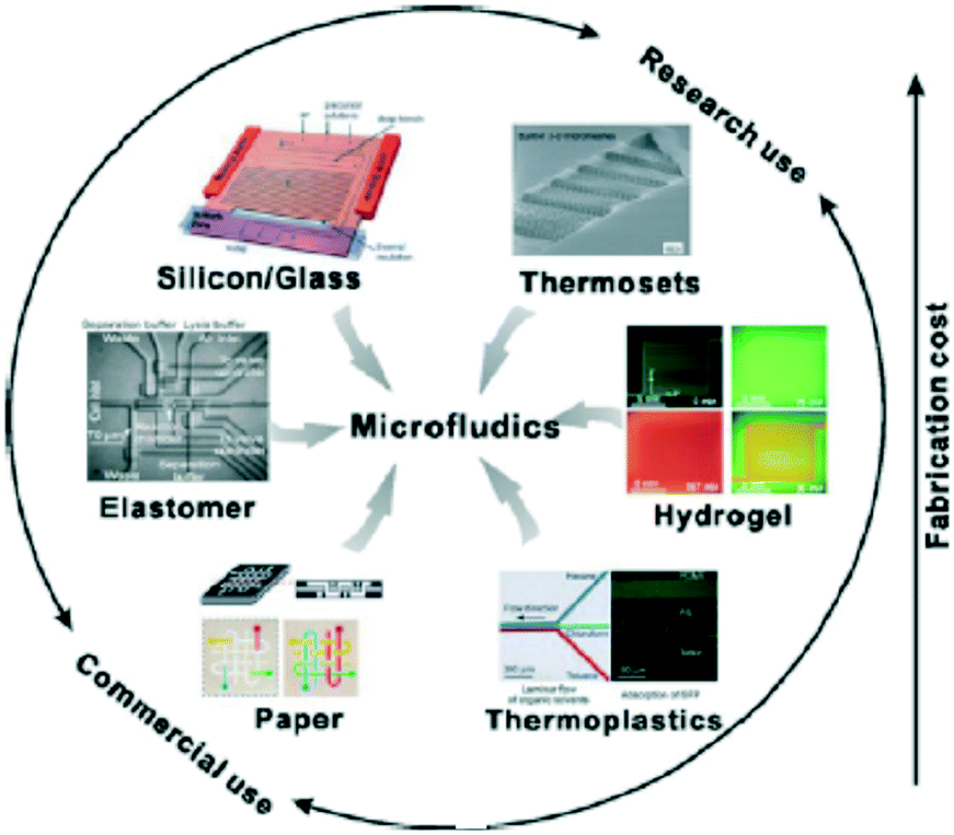 | ||
| Fig. 3 Rating of microfluidic devices with respect to fabrication cost and type of use (reprinted with permission from ref. 38, copyright 2013, American Chemical Society). | ||
2.3 Paper
Paper is one of the first materials used for biochemical assays (glucose tests, pregnancy tests, chromatography),55–57 owing to its inherent hydrophilicity, biocompatibility, low cost, white background (ideal for colorimetric detection assays) and easy disposal (natural degradation, incineration).5 Until recently, although no easy way to fabricate microfluidics had been demonstrated, microfluidic research has been dominated by polymer and glass substrates.In 2007, Martinez et al.58 first introduced a simple method of creating consistently millimetre-sized channels on paper, thus introducing a novel and exciting capability for more advanced paper-based lab-on-a-chip devices. Since then, the field has rapidly advanced with several fabrication approaches introduced:59 wax printing, inkjet printing, photolithography, flexographic printing, plasma treatment, laser treatment, wet etching, screen printing and wax screen-printing. Each technique has its advantages and disadvantages, with the lower-cost printing approaches being more promising for large scale production of POC devices.
Based on this approach, very promising microsystems (2D and 3D) and biosensors60–62 (Fig. 4A and B) have started to emerge. In terms of flow control, the hydrophilic nature of paper allows pressure-free fluidic transport; however, methods for controlling the fluid flow are still required and hence recently suggested for the implementation of more complex assays (valving, timed reagent delivery, separation, mixing).63–66
 | ||
| Fig. 4 A) Paper-based electrochemiluminescence DNA sensors (reprinted with permission from ref. 61, copyright 2013, American Chemical Society) and B) enzymatic ePAD devices (reprinted with permission from ref. 60, copyright 2009, American Chemical Society).62 | ||
In terms of biosensing, the substrate itself is an organic material with no significant optical, electrical or chemical properties that can be used for transduction.67 Hence, the integration of any kind of quantitative biosensor is the most challenging part for a full stand-alone paper-based diagnostic system. Colorimetric detection has dominated the field until now, being the easiest and most cost-effective method.68–71 The first commercial application of paper-based devices (Diagnostics For All, DFA)72 is based exactly on this approach, aiming to commercialize paper-based, low-cost point of care diagnostics in the developing world via a non-profit enterprise model.
Despite the indisputable advantage of simplicity in this effort, sensitive and quantitative results (Table 1) are still required for accurate POC diagnosis. In order to cover these specifications, integration of some kind of electronics is still under investigation in paper-based systems. Addressing this issue, electrochemical microfluidic paper-based analytical devices (μPADs) are the second most popular biosensing approach for paper substrates, printing conductive inks in order to form sensing electrodes.60,73–77
With analyte quantification being a pre-requisite for many diagnostic applications, electrochemical detection seems to be the future route to follow. Despite the efforts for developing printed electronics techniques towards this goal, there is still a lot of work to be done in a variety of fields (printable biosensors, μPAD paper, reagent storage, paper-based power systems, etc.) until a financially viable paper-based POC product providing quantitative analysis can be commercialized.67
3 Lab-on-PCB
Printed circuit boards as platforms for LoC devices claim to eliminate most of the hurdles imposed by other substrates in the commercialization of microfluidic devices and systems: upscaling, standardization, and system-level integration of microfluidic devices at a minimal cost. These advantages stem from the exploitation of the well-established PCB technology, currently routinely used for the mass production of electronic circuits and consumer electronics. It is hence suggested that the microfluidics community should seriously consider and further investigate on adapting to the PCB technology for various commercial applications in diagnostics. Such an adaptation to this fabrication technology would facilitate the standardization of microfluidic components, following the electronics paradigm, and render PCBs a platform for convenient system integration. In this section, a thorough review of the lab-on-PCB technology will be attempted, along with its historical evolution and development to present prototypes. Its particular upscaling advantages, such as the low-cost production, the current technological capabilities, and the size of PCB manufacturing market worldwide will be highlighted along with the re-sparked interest in such devices. The detailed presentation of already demonstrated lab-on-PCB microfluidics, complex μTASs and biosensors is indicative of the readiness of this technology for commercialization and standardization.3.1 Technology overview and demonstrated prototypes
Printed circuit boards are typically composed of planar insulating layers such as an FR4 core (fiberglass interwoven with an epoxy resin) and layers of conducting metal, copper most commonly (copper-clad FR4). The main processing steps of the PCB technology will be presented in detail below (section 3.2). In brief, a typical fabrication process comprises photolithography for transferring a desired design on copper, followed by wet etching of copper to form the copper tracks. Next, vias (holes) are drilled with electroplating enabling the connection between copper layers, where desired. If stacks with multiple copper layers are necessary, copper-clad FR4 is laminated together with fiber weaves impregnated with a resin bonding agent (such as epoxy) and bearing copper foil. Today in industry, multilayer PCBs with up to 24 layers are available with standard processing, extending the capability of processing up to 40 layers for prototypes.78 In addition, fabrication of flexible printed circuits (FPC) and combinations of flexible and rigid (flex-rigid) printed circuits are also possible in industry. Therefore, microfluidics fabricated on flexible, mostly polyimide (PI) sheets will be also reviewed here. Apart from the interesting advantages of the PCB technology in terms of cost, fabrication service, large scale production, reliability and electronic integration, these substrates (FR4, PI) have excellent thermal stability, good mechanical and electrical properties and resistant to most of the commonly used reagents. Last but not least, recycling and disposal facilities are already available and used in the PCB industry, alleviating environmental concerns for the use of disposable lab-on-PCBs. Below, prototypes of both microfluidic systems and sensors, realized by implementing basic processing steps of the PCB technology, will be reviewed.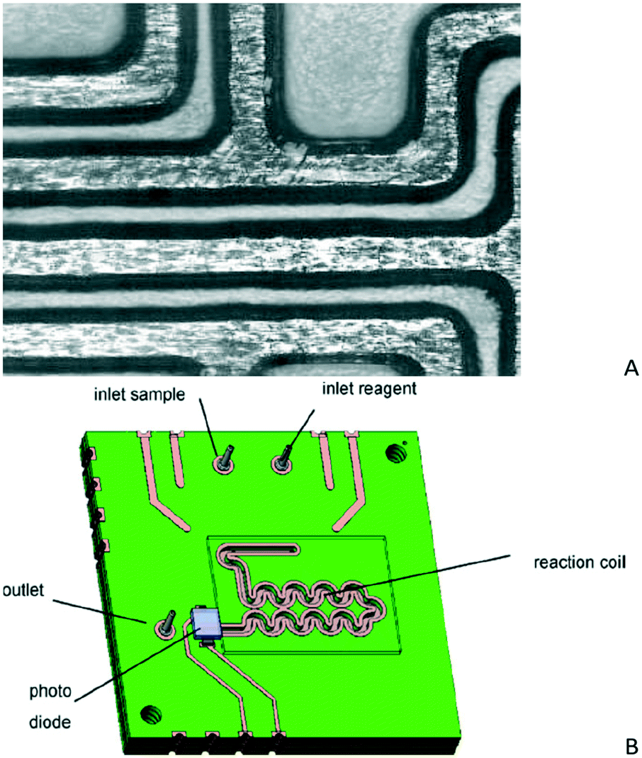 | ||
| Fig. 5 A) Fluidic channels on a PCB covered with glass (reprinted from ref. 82, copyright 1999, with permission from Elsevier) and B) model of a fluid injection analysis system designed for fabrication on a PCB (reprinted from ref. 85, copyright 2007, with permission from Elsevier). | ||
For example, SU-8 has been extensively used for the formation of microfluidic channels or chambers on top of the PCB. First, the electrical components are fabricated on a PCB and then an SU-8 layer is coated on the PCB to planarize and aid the adherence of the fluidics which are subsequently patterned in an additional SU-8 layer. In one case,86 platinum (Pt) resistors were fabricated on a PCB (by Pt sputtering followed by a lift-off process) to serve as temperature sensing elements. A microfluidic flow channel was then patterned on a second layer of SU-8 (Fig. 6A). Afterwards, a thin layer of PMMA was spin-coated on the surface of the SU-8 channels which were sealed with a thick PMMA plate by thermal bonding. The method was used for the fabrication of a PCB-based flow sensor allowing for the integration of the sensor electronics on the same board with flow channel and sensing elements. In other cases, an electroosmotic micropump,87 an electrochemical-sensor cell array88 and a single-use, low-consumption microvalve89 were fabricated by integrating the microfluidic channels on the SU-8 layer with electrodes and electrical connections on the PCB. The single-use microvalve was later integrated into an on-chip impulsion system (Fig. 6B) for autonomous micromixing, preventing the use of external pumps and greatly improving the system portability.9 Despite the enormous integration possibilities offered by the combined PCB/SU-8 technology in the realization of lab-on-PCB systems, the industrial upscaling of this technology seems at the moment limited by the high degree of process modifications required to be adopted by the PCB industry. In addition, the SU-8 technology lacks the high yield and productivity which is of utmost importance for industry.
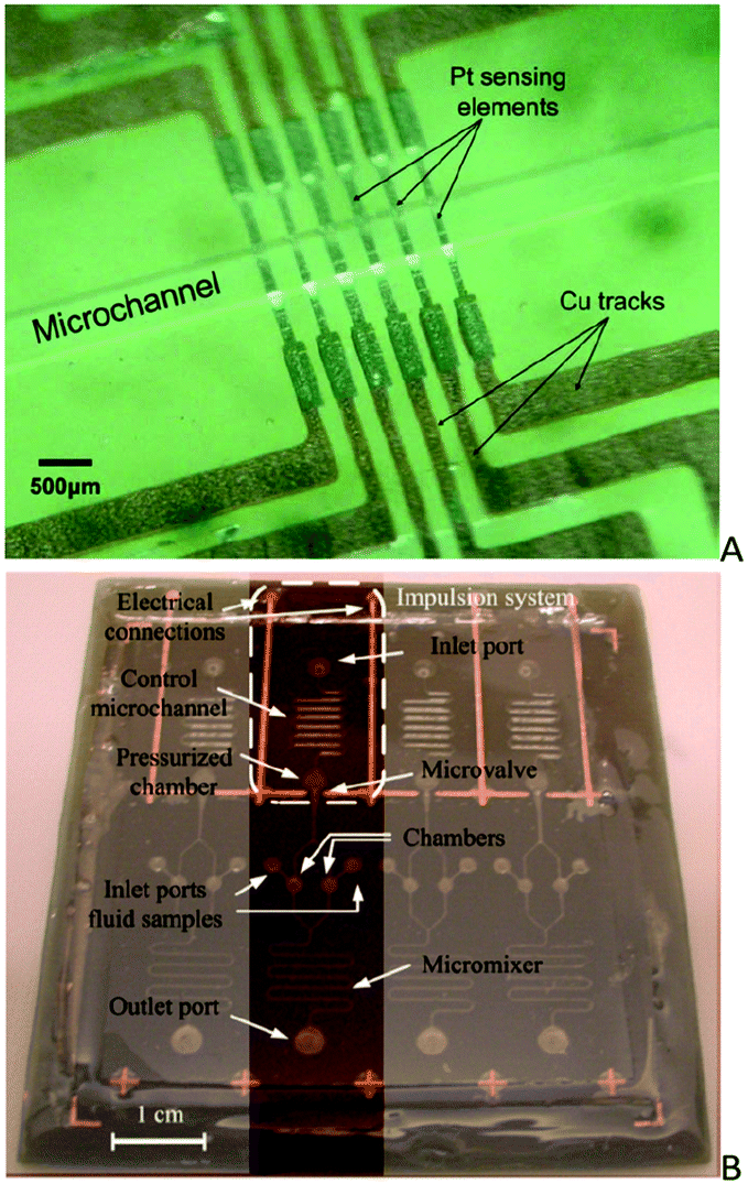 | ||
| Fig. 6 A) Image of the low-sensing elements and SU-8 microchannel integrated into the PCB (reprinted from ref. 86, copyright 2009, with permission from Elsevier) and B) image of the lab-on-PCB platform for autonomous micromixing (reprinted from ref. 9, copyright 2015, with permission from Elsevier). | ||
To overcome these deficiencies of SU-8, dry film photosensitive resists (DFR) have been proposed, motivated by the success of the DuPont™ Riston® dry film photoresist, which revolutionized the way printed circuit boards were fabricated, when it was invented 40 years ago.90 Generally speaking, DFRs are more advantageous compared to liquid resists, due to the high yield and quality of their processing through uniform resist thickness and the high productivity through elimination of drying and edge-bead removal.91 Recently, TMMF, 1002F or Ordyl DFRs have been proposed and used for planarization, encapsulation, and creation of the microfluidic network and sealing on PCB substrates. Specifically, TMMR S2000, also called TMMF S2000 when sold as a dry resist from Tokyo Ohka Kogyo Co., Ltd., was used to create microfluidics on a PCB surface.92 The patterning of the fluidics was achieved by UV exposure, development and baking. The channels were finally sealed with a second layer of TMMF which was also exposed and cured93 to provide fluidic interconnections for a nanofluidic chip integrated into the PCB. Despite the fact that in the latter work the nanofluidic chip was fabricated on Si and thus the overall chip was a hybrid one, an attractive platform is provided for integration of Si-based chips with PCB-based fluidic and electrical connections. Another dry resist, the 1002F polymer, was used94,95 to planarize and encapsulate surface mounted components (resistors, LEDs, temperature sensors) on top of a PCB surface by casting the 1002F polymer and using a hot press and UV exposure. A second layer of 1002F was used for the fluidic patterning by UV lithography. The sealing of the device was achieved using a lamination process using tape or a thin layer of the cured 1002F polymer. Finally, Ordyl DFR was applied96 for the fabrication of microfluidic chips for capillary electrophoresis with integrated PCB electrodes, implemented for capacitive contactless conductivity-based detection. In this work also, the final devices were hybrids, using a PDMS slab either hosting the microfluidic network or sealing the device.
While it remains to be seen whether or not these DFRs will be adopted by the PCB industry, thus facilitating the commercialization of low-cost lab-on-PCB systems, the integration of rigid substrates into PCBs has been also proposed. In fact, hybrid LoC devices have been fabricated by combining a PCB with other hard substrates such as glass, polycarbonate (PC), cyclo-olefin copolymers (COCs), cured epoxy chips, or soft PDMS. For example, a glass–PCB hybrid device has been reported,97 where the fluidic part was fabricated on glass by means of SF6 plasma etching and bonded onto a thin PI (Pyralux-AP Polyimide, Kapton®) with the aid of a PDMS elastomer membrane, irreversibly bonded on the PCB by means of a siloxane-based surface adhesion promoter.98 In such hybrid systems, on-chip storage and dispensing of liquids99 are also made possible through the use of integrated heaters implemented for example as paraffin actuators. In such hybrid devices, integration of Si transducer chips (for conductivity-based or pH detection) has been also made possible together with microfluidics fabricated in PDMS.100 Disposable PDMS–PCB chips were also reported for electrophoretic separation and amperometric DNA detection101 or low cost detection and enumeration of circulating tumor cells in a microfluidic impedance cytometer.102,103 In addition, highly integrated microfluidic components and LoC devices have been developed on PCB substrates for on-chip sample preparation, DNA amplification and detection, by integrating multiple embedded heating and sensing elements together with electrical circuitries on a PCB with a polymeric cover where the microfluidic network (mixers, valves, pumps, etc.) was micromilled.104 For example, an elaborate PCB-based sample preparation module (with the fluidics on polyurethane, PU) has been presented from Stanford University,105 for the extraction of pathogenic nucleic acids directly from raw blood, demonstrating that it is feasible to have this integral part of lab-on-a-chip diagnostics on a PCB platform. Using a similar hybrid technology, impressive fully integrated, self-contained LoC devices were reported106 (Fig. 7), such as the “FraunhoferivD platform”107 for sample preparation, DNA amplification and detection, in combination with a fully automated instrumentation, for rapid disease diagnosis. A much simpler microfluidic chip on which the microchannels and the microelectrodes of sensors were integrated directly into the copper sheet on a PCB was demonstrated for the generation of oil-in-water and water-in-oil emulsion droplets.108 More recently, a novel concept and application has been proposed in a hybrid chip for microfluidic thermal treatment of water, realized in hybrid PC–PCB chips.109 As it becomes evident from the above discussion, the combination of PCBs and polymeric, functional covers has proved an excellent solution towards the realization of highly integrated, self-contained LoC devices and systems.
 | ||
| Fig. 7 Self-contained LOPCB integrating reagent storage, valves, pumps, microheaters, PCR chambers and DNA microarray sensors for pathogenic bacteria detection from whole blood (reprinted with permission from ref. 106, copyright 2004, American Chemical Society). | ||
In most of the above mentioned works on the fabrication of lab-on-PCB systems, the microfluidic network is fabricated in materials (SU-8, TMMF, 1002F, Ordyl, PDMS, etc.) not commonly used in the PCB industry, requiring the introduction of new materials and modified processes for upscaling. An interesting exception to the above works is the work of the Rostock group81,82,85,110 that implements a multilayer standard PCB technology without additional process steps, as well as of those of a few other groups (work to be described below) implementing only materials with which the PCB industry is quite familiar, i.e. rigid PCB, flexible PI, photosensitive PI-based dry films, and other laminates. For example, pioneering work on the fabrication of microfluidic channels integrated with electrodes was carried out at EPFL on flexible metalized polyimide films (also currently implemented in the PCB industry).111 A photosensitive PI (PI-2732, DuPont) patterned by means of lithography or a non-photosensitive type PI (PI-2611, DuPont) patterned by dry etching techniques was implemented for the formation of microfluidic structures. The sealing process that followed used N-methyl-2-pyrrolidone solvent (NMP, a swelling agent for PI) in order to modify the surface of polyimide and facilitate irreversibly strong bonding with another PI foil. Another non-photosensitive type of polyimide (Pyralux™ from DuPont) was microstructured by means of plasma etching (O2/SF6) for the fabrication of a meander-like microchannel, lying above three resistive copper microheaters for performing DNA amplification based on polymerase chain reaction (PCR). The microchannel was sealed using polyolefin thin tape bearing a pressure sensitive poly(dimethyl)siloxane (PDMS) adhesive112 and the microheaters were used also as temperature sensors to indicate the correct temperatures necessary for PCR.113 Similarly, an improved continuous flow PCR device was fabricated using the same patterning method and materials, but the sealing was performed using commercially available Kapton® PI tape with a siloxane adhesive.114 In this device, sufficient amplification of a DNA fragment (90 bp) was demonstrated within 5 min, with relatively low power consumption (2.5 W). This was achieved due to the small thickness of the substrate and the careful design of the device, targeting sufficient temperature uniformity (set-point ±1.5 °C) across each thermal zone.
DFRs with which the PCB manufacturers are mostly familiar are the polyimide-based laminated dry film resists (e.g. PC1000), routinely used in the PCB industry as solder masks. These materials were recently implemented in research labs as patterning layers on top of commercial PCBs for the fabrication of microfluidic components to be integrated into LoCs. For example, micromixers of various geometries have been fabricated, after sealing with thin polyolefin films.115,116 Furthermore, microfluidic devices for DNA amplification have been fabricated on 4-copper layer PCB substrates by using either CNC machining or photolithography of industrially used dry film photosensitive resists, for the formation of meandering microfluidic channels.117,118 In the latter work also, copper facilitates the incorporation of on-chip resistive microheaters, serving both as thermal zones necessary for DNA amplification (Fig. 8A) and as temperature sensors114 implemented for temperature regulation. In a few cases, integration of semiconductor biosensing chips with PCB-based microfluidics and sensor read-out electronics was demonstrated for the creation of integrated, yet hybrid LoCs.119,120 For this reason, sensors fabricated on a PCB by the standard PCB technology are highly desirable for seamless integration and upscalability of PCB-based lab-on-chips and will be reviewed below.
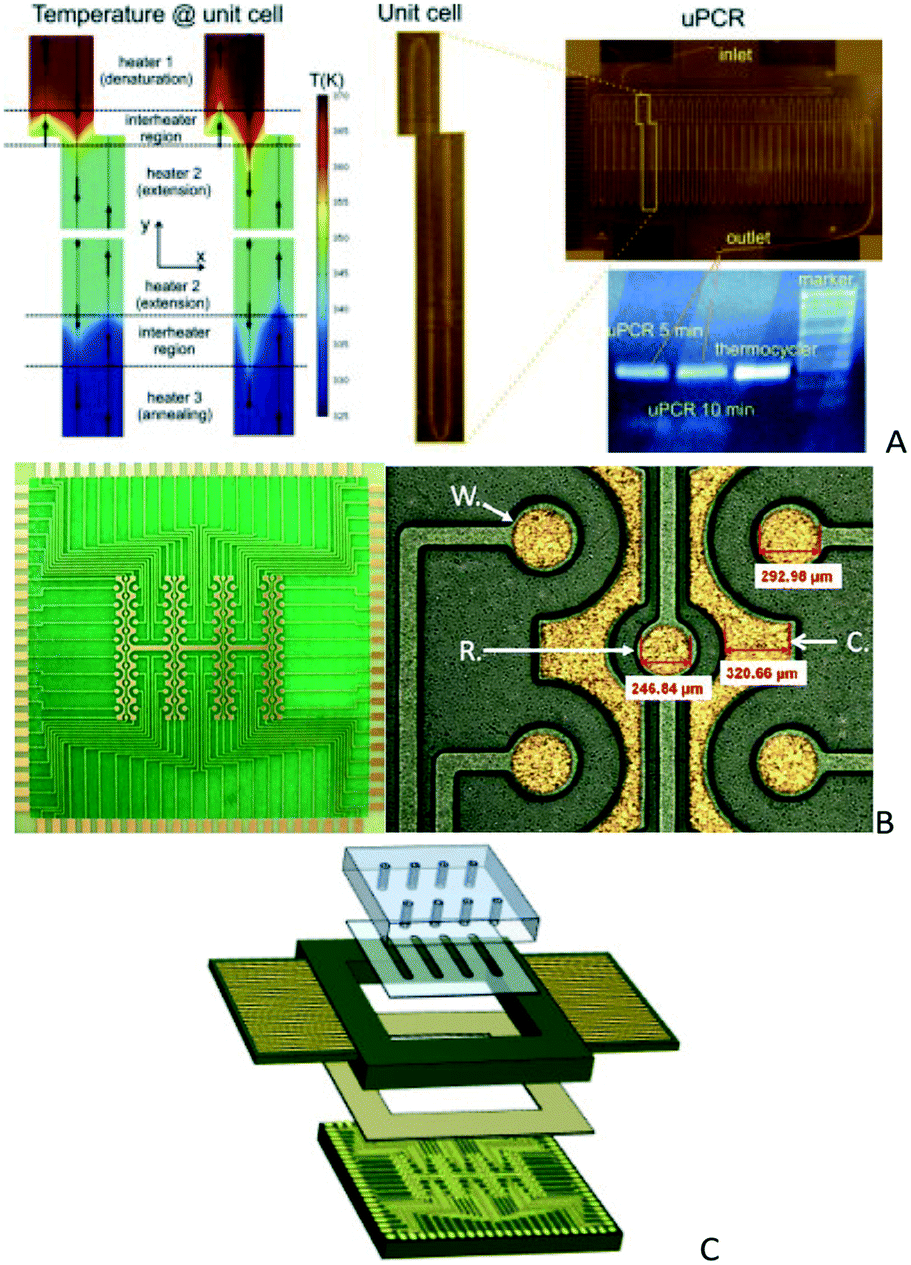 | ||
| Fig. 8 A) Integrated uPCR-on-PCB (reprinted from ref. 114 with permission from Elsevier) and electrochemical biosensor array chips on a PCB, B) an electrolytically gold plated DNA detector on a PCB (from ref. 131, with permission from IOS Press) and C) a schematic representation of the sensor platform B packages with PMMA microfluidics (reprinted from ref. 132, copyright 2016, with permission from Elsevier). | ||
Further applications of the PCB technology in the LoC field include droplet-based microfluidics and the fabrication of master molds. Indeed, PCBs have been employed as substrates in two-dimensional (digital) microfluidics,121 which is the basic technology of Advanced Liquid Logic Inc.,122 in which multilayered electrical access lines are used for electrowetting on dielectric (EWOD) movement of droplets and automated liquid handling. A PCB-based capacitive fluidic sensor was also reported by Vu Quoc et al.123 for real-time monitoring of air bubbles in microfluidic channels. Finally, copper-clad PCB substrates can be employed to produce,124 at low cost, high speed and with simplicity, master molds for the fabrication of polymeric microfluidic devices.
A hybrid approach, integrating a CMOS-based ISFET sensor via wire bonding into a PCB microfluidic platform, was presented by Tseng et al.126 for fast (within 2 min) diagnosis of glucose-6-phosphate dehydrogenase (G6PD) deficiency in blood samples. This approach exploits the increased ISFET sensitivity in sensing small changes in pH, in this case caused by the reduction of nicotinamide adenine dinucleotide phosphate (NADP) in the presence of the G6PD enzyme. While such an integration strategy benefits from a sensitive and robust CMOS based sensor, it stills presents difficulty in its upscalable production, requiring wire bonding of the CMOS chip on the PCB substrates, and in the fluidic sealing process.
The work presented by Prodromakis et al.127 presents a solution to this issue, exploiting pH sensitive, PCB based extended gate ISFETs. The PCB based TiO2 pH sensors demonstrated a sensitivity of 22 mV pH−1, but nonetheless in terms of fabrication still required clean room based post-processing for the pH sensing TiO2 membrane. Addressing this issue, the group replaced the TiO2 sensing membrane with a PCB technology compatible material, namely, Parylene-C,128 while improving the extended gate ISFET sensitivity to 16.3 mV pH−1.
A PCB-based electrochemiluminescence device for the quantification of H2O2 has also been presented by Pittet et al.,129 presenting detailed electrochemical characterization of gold vs. gold and gold vs. Ag/AgCl PCB electrodes. In all of the aforementioned papers, there is still a need to exploit a discrete Ag/AgCl reference electrode. Moschou et al.130 addressed this issue, studying the PCB compatible fabrication of integrated Ag/AgCl reference electrodes. The PCB integrated reference electrodes proved electrically stable in an unbiased mode operation, thus allowing their exploitation in open circuit potentiometry experiments.
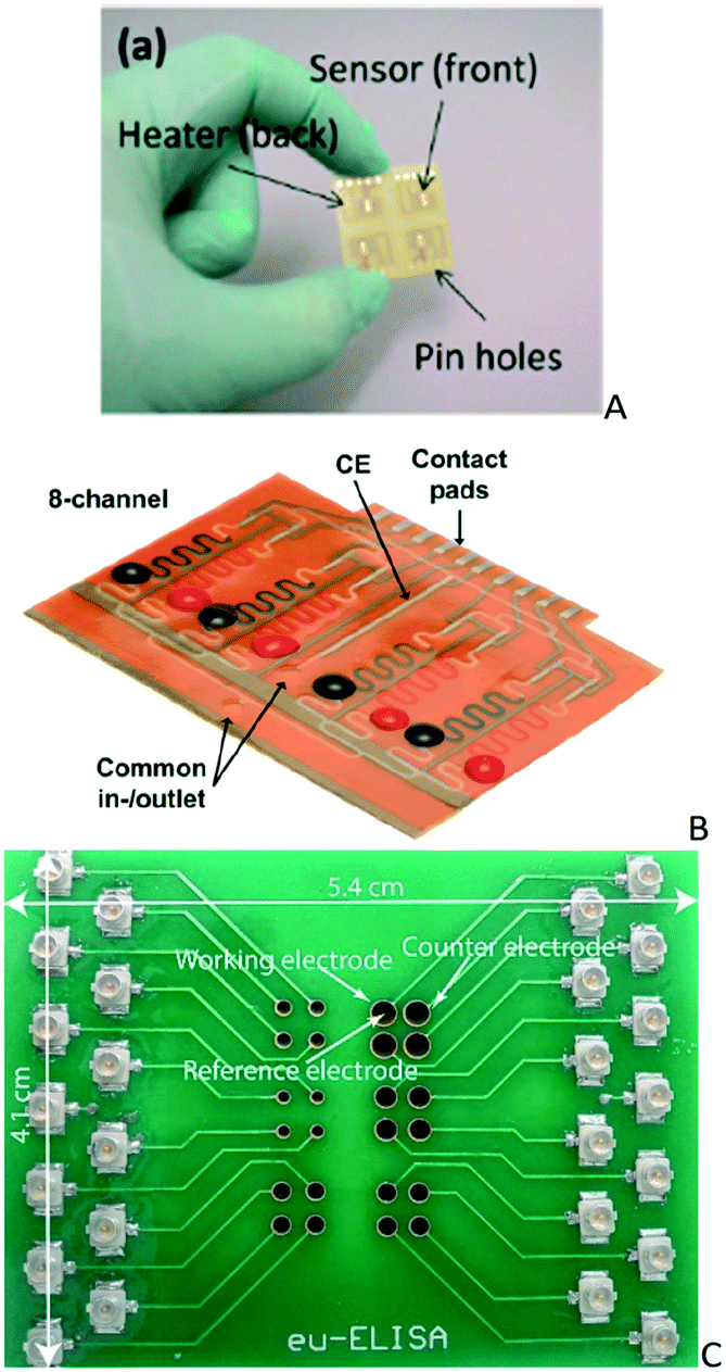
PCB based biosensors have also been successfully exploited in biochemical sensing of clinically relevant biomarkers. IMEC (ref. 131) presented in 2014 a study of PCB gold electrodes (Fig. 8B) exploited for the detection of DNA breast cancer related biomarkers, highlighting the cost effective upscalability advantage of this technology. In this work, a detailed study of the gold plating process was performed, presenting a threefold improvement in the detection limit (0.05 nM) over clean room fabricated sensor platforms and high specificity.
Expanding these highly promising results, Sanchez et al.132 demonstrated in 2016 multiplex electrochemical detection of seven breast cancer genetic markers on the same PCB-based gold electrode array, integrating also Peltier heating elements and laser machined PMMA microfluidics (Fig. 8C). In this work, the authors also highlight the importance of the gold plating process (soft gold layers over nickel vs. electroless nickel with immersion gold) in the controlled immobilization of the capture receptors. Hence, in this work, the array-to-array and sensor-to-sensor reproducibility proved excellent, while achieving 25 pM limit of detection.
A compact biosensing system was presented by Tseng et al.133 that contained an array of devices comprising three-microelectrode electrochemical sensors (Fig. 9A) and resistive heaters, intended for employment in quantitative polymerase chain reactions. Despite the impressive DNA biosensor PCB systems proposed, no fully PCB compatible molecular diagnostic LoC has been demonstrated to date.
 | ||
| Fig. 9 A) PCB integrating electrochemical sensors and microheaters (reprinted from ref. 133, copyright 2014, with permission from Elsevier), B) photographs of the antibiotic detection microfluidic biosensors comprising eight immobilization sections (reprinted from ref. 136, http://pubs.acs.org/doi/full/10.1021/acs.analchem.6b02294) and C) commercially fabricated microchambers used for IFN-γ detection (reprinted from ref. 137, copyright 2016, with permission from Elsevier). | ||
PCB biosensors have also been studied extensively for protein biomarker detection. Hybrid PCB technologies have been employed, post-processing the PCB electrodes in an effort to increase their sensitivity. Nanotextured ZnO thin films, sputter-deposited on a PCB, providing ultrasensitive detection of troponin-T for cardiovascular diagnostics134 were reported by Jacobs et al. An electrochemical sensor was developed on a flexible PCB, incorporating a nanostructured electrode surface modified by graphene and gold nanoparticles to achieve enhanced sensitivity in glucose detection.135
In 2016, Prof. Urban's group136 at the University of Freiburg presented a flexible PCB-based (Dupont, Pyralux AP8525R) electrochemical microfluidic platform for multianalyte antibiotic detection (Fig. 9B). In this last approach, DFRs are exploited for the microfluidic layer, rendering the microfluidic part PCB compatible as opposed to the two previous ones. However, the authors choose not to use the already present metal layer for electrochemical detection but instead deposit platinum electrodes, thus adding a non-standard PCB processing step to the system fabrication flow. A glucose oxidase assisted amperometric assay is implemented on the sensing electrodes, detecting protein targets of two antibiotic classes (tetracycline, LOD = 6.33 ng mL−1 and pristinamycin, LOD = 9.22 ng mL−1) in human serum.
Nonetheless, purely PCB-based sensing electrodes for protein detection have also been demonstrated. During the same period, Moschou et al.137 demonstrated the successful exploitation of PCB sensing electrodes for IFN-γ sensing (Fig. 9C), realized on fully integrated, commercial multi-layer PCBs,130,137–139 intended for employment in a fully integrated immunodiagnostic chip137 in combination with commercially fabricated DFR-based microfluidics.139 Also in 2016, Moreira et al.140 studied silver plated PCB electrodes for the electrochemical impedance spectroscopy-based detection of carcinogenic embryonic antigen protein. In this work, an antibody-like biomimetic material is used as a sensing element, demonstrating excellent specificity and a dissociation constant of 0.0058 ng mL−1.
In the work of Li et al.,141 an integrated PCB based array sensing chip with a high signal to noise ratio and a high sensitivity was developed for simultaneous detection of lactate and glucose in serum. In this case, lactate oxidase and glucose oxidase were immobilized on gold plated electrodes, and the amperometric response was recorded for increasing lactate/glucose concentrations. The achieved sensitivity in both of the latter biosensors promises lab-on-PCB diagnostic systems with high sensitivity, specificity and reproducibility, provided a PCB compatible microfluidic is integrated.
3.2 Upscaling advantages
The academic-led research so far demonstrates the feasibility of fabricating required lab-on-a-chip components and systems exploiting the PCB technology, as is the case for all of the other fabrication technologies suggested until now. The unique, competitive advantage of the lab-on-PCB approach over the alternatives currently pursued lies in its inherent low cost upscalability for fully integrated LoCs and the benefit of a large, long-standing industry already available.The printed circuit board, the platform upon which components such as semiconductor chips and capacitors are mounted, was built to provide electrical interconnections between electronic components. Being a very mature industry with more than 60 years of technology development (the first double-sided PCB was manufactured in 1947 (ref. 142)), process standardization and infrastructure investment, commercially fabricated PCBs are now increasingly complex: multilayer, flexible or flexi-rigid hybrids, evolving into high technology products and starting to compete with the micrometer scale technology of the semiconductor industry.143 At the same time, this industry benefits from much lower infrastructure and processing costs; indicatively, a single layer PCB can be individually purchased for $0.20 per cm2, while a 4 layer board can be purchased for $0.52 per cm2, as opposed to glass microfluidic chips that cost on the order of $10–20 per cm2. This cost estimate clearly indicates why this technology could be leveraged for applications such as point-of-care diagnosis: the cost is similar to paper and CMOS fabricated chips, but featuring increased functionalities and with no additional costs for chip-to-world connectivity, packaging or electronics integration; PCBs produced from the factories are ready to be used. The cost of PCBs can be reduced even further in large-scale production, since industry works following the panelization concept, thus allowing parallelized manufacturing in large quantities.
The industrial processes relevant to lab-on-PCB fabrication and currently exploited for the standard PCBs can be summarized as follows.
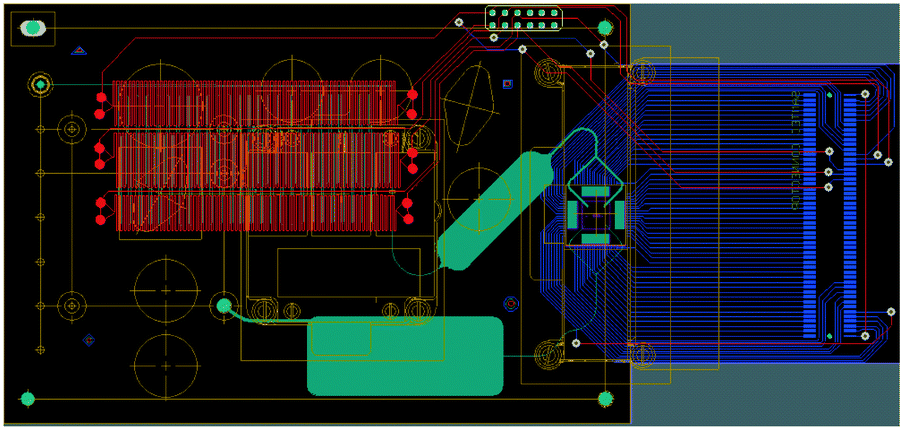 | ||
| Fig. 10 Multilayer lab-on-PCB design incorporating instrumentation mechanical specifications, metal layers and an electronic interfacing and microfluidic network (reproduced with permission from Chemical and Biological Microsystems Society, ref. 144). | ||
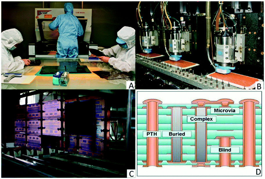 | ||
| Fig. 11 A) Photopatterning of the resist, courtesy of EPEC;145 B) CNC drills, courtesy of EPEC;145 C) industrial wet processing line (© Swoolverton/Wikimedia Commons/CC-BY-SA-3.0, ref. 147); D) schematic of the different via configurations (courtesy of EPP Europe148). | ||
| Application | Sensor technology | Microfluidic technology | Non-standard PCB fabrication steps | Ref. |
|---|---|---|---|---|
| Glucose & lactate detection | Electrochemical (amperometric) | DFR | Sensor integration | 8 |
| Volume actuator | Capacitance bubble detection | Copper patterning | PCB compatible | 7 |
| pH regulation for cell cultures | Optical pH sensor | Copper patterning | Sensor integration | 82 |
| Micropump | Copper patterning | Heating wire and thin foil integration | 83 | |
| Micropump | Copper patterning | PCB compatible | 84 | |
| Flow injection analysis (Fe3+) | Optical (480 nm diode) | Copper patterning | Chip interfacing | 85 |
| Flow rate sensor | Pt resistive sensors | SU-8 | SU-8, Pt deposition, polymer sealing | 86 |
| Electroosmotic pump | SU-8 | SU-8 | 87 | |
| DNA sensing | Electrochemical (chronopotentiometry) | SU-8 | SU-8, gold wire bonding | 88 |
| Microvalves | SU-8 | SU-8 | 89 | |
| Microchannels | DFR | Nanofluidic (Si-based) integration | 93 | |
| Electroosmotic flow | DFR/liquid polyurethane | PDMS sealing/liquid polyurethane | 94 | |
| Capillary electrophoresis | Electrochemical (capacitively coupled contactless conductivity detection) | DFR | PDMS sealing | 96 |
| Glass | Sensor integration, PDMS sealing | 97 | ||
| On chip reagent storage & dispensing | Epoxy | Microfluidic sealing | 99 | |
| DNA detection | Electrochemical (amperometric) | PDMS | PDMS bonding | 101 |
| Coulter counter | Electrochemical (impedance) | PDMS | PDMS bonding | 102 |
| DNA detection | Electrochemical (AC voltammetry) | PC gasket | Gasket sealing | 104 |
| Bacterial DNA detection | Electrochemical (eSensor™ microarray) | PC | PC microfluidic & sensor integration | 106 |
| CRP/PSA protein markers | Electrochemical (chronoamperometry) | COC | COC microfluidic & sensor integration | 107 |
| Emulsion droplets | Capacitance detection | Copper | Microfluidic sealing | 108 |
| Seawater sample thermal cycling | PC | Microfluidic sealing | 109 | |
| DNA amplification and detection | Electrochemical (SWV) | FR4/pre-preg | PCB compatible | 110 |
| Biological tissue interfacing | Electrochemical (muscle recordings) | DFR | PCB compatible | 111 |
| DNA amplification | PI | Plasma etching | 112 | |
| DNA amplification | PI | Plasma etching | 114 | |
| Enzymatic digestion | DFR | Microfluidic sealing | 115 | |
| Enzymatic digestion | DFR | Microfluidic sealing | 116 | |
| DNA amplification | FR4 | Microfluidic sealing | 117 | |
| pH | Electrochemical (IDE & ISFET) | PDMS | PC microfluidic & sensor integration | 100 |
| Colon cancer | Electrochemical (capacitive) | DFR | Sensor integration | 120 |
| Glucose sensing | Electrochemical (amperometric) | DFR | Sensor integration | 125 |
| G6PD deficiency | Electrochemical (ISFET) | PDMS | PDMS microfluidic & sensor integration | 126 |
| pH sensing | Electrochemical (extended gate ISFET) | Sensing layer deposition | 128 | |
| H2O2 sensing | Electrochemiluminescence | DFR | Microfluidic sealing | 129 |
| pH sensing | Electrochemical (OCP, extended gate ISFET) | PMMA | PMMA sealing | 130 |
| DNA sensing | Electrochemical (amperometric) | PCB compatible | 131 | |
| Quantitative DNA amplification | Electrochemical (cyclic voltammetry) | SU-8 | Microfluidic sealing | 133 |
| Troponin-T detection | Electrochemical (EIS) | PDMS | ZnO deposition, PDMS bonding | 134 |
| Glucose detection | Electrochemical (amperometric) | PDMS | Graphene inkjet printing, gold nanoparticle electrodeposition, PDMS bonding | 135 |
| Antibiotic detection | Electrochemical (amperometric) | DFR | PCB compatible | 136 |
| Tuberculosis | Electrochemical (amperometric) | PMMA | PMMA bonding | 137 |
| Passive microfluidics | DFR | PCB compatible | 139 | |
| Cancer biomarker detection | Electrochemical (DPV) | PCB compatible | 140 | |
| Lactate & glucose detection | Electrochemical (amperometric) | PCB compatible | 141 | |
| Cell lysis and nucleic acid extraction | Polyurethane | Microfluidics bonding | 105 | |
| Electrowetting on dielectric | Teflon/ITO deposition | 121 |
Patterned metal areas of the boards that do not require electrical connectivity (e.g. metal routes) can be coated with an electrically insulating solder mask layer serving also as protection from the environment, either by screen printing or by means of a photosensitive laminate.
This capability offers unique versatility in the lab-on-PCB technology, allowing for the fabrication of 3D LoCs through a combination of various material layers at will or even flexible/flexi-rigid microsystems. While pre-preg layers are routinely used at the moment for mechanical adhesion of electrical layers, an adaptation of this bonding technique (bonding temperature/pressure/time, material optimization, substrate pre-treatment) can be exploited for fluidic sealing of PCB microfluidics.
The described fabrication technology is very similar to the routinely exploited microfabrication processes in lab-on-a-chip microsystems, offering a wide range of materials and process combinations to achieve the desired result, but this time on an industrial scale, following processing according to international standards149 and regulations.143 The final cost of each device will be defined by the exact process and material requirements but would be expected to be below $1 per cm2, given the current costs of electronic PCBs. Therefore, footprint should also be a consideration for lab-on-a-chip designers, since the final cost is directly associated with the area of the board and the number of individual boards fitted in each panel. In the lab-on-PCB case, no particular consideration for electrical interfacing or packaging needs to be considered, as is the case for all alternative integration technologies; slot type interfacing (e.g. PCI express, flat flexible connectors) is routinely used already in PCBs. On the fluidic side, already available fluidic connectors can be easily attached to the boards (e.g. luer type) or directly interfaced by means of O-rings or ferrules,150 assuring fluidic tightness.
3.3 Lab-on-PCB industrial status
Quoting Dr Nge:5 “Highly integrated systems must be developed in a way that enhances performance and reduces costs relative to conventional methods”; the lab-on-PCB aspires to address these exact points by adding effortlessly electronic functionality in lab-on-a-chip systems while reducing their upscaling cost to practical levels; to this end, the established position of the PCB industry in the world is of critical importance.Currently, the global PCB market is valued over $59.2 billion, with Europe sharing a 4.1% market share, mostly aimed at high specification products (aerospace, automotive applications). Most globally leading PCB manufacturers are located in Asia (e.g. Nippon Mektron, ZDT, Unimicron) with turnovers on the order of $2–3 billion and impressive annual growths (>10%). The top 74 largest European PCB companies totalled more than $1 billion in turnover in 2015. Given the projected aggressive growth and increasing market value of POC (global POC market currently estimated in excess of $15 billion annually with an annual growth of 7%) and LoC (projected market growth at 18–29%, reaching $3.6–5.7 billion by 2018) technologies, the PCB industry aspires in adapting accordingly and leveraging its existing technical and commercial infrastructure to address this need. The European Institute of Printed Circuits (EIPC) announced its new activities in MEMs, during Electronica 2016 in Munich; the inaugural event was the first PCB BioMEMs workshop,151 followed by a business to business joint event between the Microfluidics Consortium (MF-8) and EIPC member industries. These initiatives aim to encourage further synergies between PCB manufacturers and the microfluidics industry.
Both Dyconex Ltd.152 and Epigem Ltd.153 are already providing microfluidics solutions based on the PCB technology, while Tulip Group154 has partnered with Bigtec Labs155 to commercialize the Truelab™, a PCB-based micro PCR system under their company, Molbio Diagnostics, thus meeting its objective of providing high quality diagnostic tools, at affordable prices, for the health care needs of the developing world. Furthermore, several academia/PCB industry partnerships have produced/are developing industrially manufactured PCB prototypes.116,117,130,137–139,156–158 Given the novelty of this approach and its commercial interest, there has been significant activity in patenting related innovations, ranging from PCB microfluidic processing to fuel cell microsystems.159–168
In the past, a few collaborations have been established between academia/research groups and the PCB industry towards industrially manufactured (rigid or flexible) PCB prototypes for microfluidics and MEMS. Examples include the collaboration of the Univ. of Rostock with ANDUS electronic GmbH for the development of a DNA amplification and detection chip109 as well as for the incorporation of PCB-based pressure sensors in commercial Sauter AG VAV controllers.169 Currently, a collaboration between the University of Seville170 and Biomedal S. L. promotes PCB-based LoC for gluten detection. Furthermore, the authors' groups are expanding their collaboration with the EIPC171 and MF-8,172 in order to raise awareness within the academic community, the microfluidics industry and the European PCB manufacturers about the capabilities and potential of the lab-on-PCB technology. We are also working with one of the most innovative PCB manufacturers in the UK, namely, Spirit Circuits Ltd.,173 aiming to adapt our technology to current industrial standards and take it a step further towards large scale production.
4 Future outlook
Convincing the wider community of the upscaling potential of PCB manufacturing, adapted to microfluidics/LoC production, would lead to researchers/engineers designing their prototypes using already existing PCB CAD/CAM and mass-producing them via the PCB industry, by simply supplying their designs to the manufacturers. Thus, a new business model for the μTAS community could be established, similar to the integrated circuit industry: end-user specifications → μTAS chip design → “tape-out” following the PCB manufacturers' standardized technology and design rules.One could think that such a business model is very close to realization, since most of the processes and tools are already there; nonetheless, in order to truly take this technology to full-scale commercialization, coordinated optimization steps need to be implemented. An ITRS-like technology roadmap could assist to this end, setting the current and future technological challenges for lab-on-PCB researchers and manufacturers.
PCB manufacturing processes need to be adapted to assure optimum yield, uniformity and reliability for high specification applications like LoC, while maintaining the processing costs to a minimum. Research should be focused on standardizing a robust fluidic sealing process at a panel level, both in terms of materials and process parameters. Metal plating processes need to be thoroughly characterized (plating thicknesses, molecular composition, surface roughness) and optimized for biosensing applications. PCB CAD/CAM would have to be adapted to cover for microfluidic design (i.e. microfluidic component design libraries) and relevant design rules should be defined and implemented to assist the LoC designers. Cost models for the lab-on-PCB technology should be clearly defined along with relevant regulations and accreditations, in order to cover the end-user specifications (e.g. pharmaceutical, food, security industries).
Equally crucial for the commercialization of this technology is the active involvement of the wider LoC scientific community, exploring the limitations of this technology for a wide variety of applications already presented. More proof-of-concept prototypes should be adapted to the lab-on-PCB technology, defining future process requirements (e.g. biocompatibility of materials, process thermal budget) and contributing to the currently unforeseen innovative ideas for different applications.
5 Conclusions
Commercialization of lab-on-a-chip devices is currently the “holy grail” within the μTAS research community. While a wide variety of highly sophisticated chips, which could potentially revolutionize healthcare, biology, chemistry and all related disciplines, are increasingly being demonstrated, very few are or can be adopted by the market and reach the end-users. The major inhibition factor lies in the lack of an established commercial manufacturing technology for the currently pursued materials (Si, glass, polymers, paper), allowing the cost-effective integration of all necessary components.The lab-on-PCB approach, while suggested many years ago, only recently has re-emerged as a very strong candidate, owing to its inherent upscaling potential: the PCB industry is well established all around the world, with standardized fabrication facilities and processes, but commercially exploited currently only for electronics. For this reason, complex μTAS integrating microfluidics, sensors, and electronics (biosensors, signal conditioning circuits, flow-control structures) on the same PCB platform can easily be upscaled, exploiting this already well-established infrastructure. In this article, we presented for the first time an overview of the demonstrated proof-of-concept lab-on-PCB prototypes to date, by the global research community. The mass-manufacturing process capabilities currently available within the PCB industries were also presented, along with the PCB industry's long-established position in the global economy. Efforts to develop a standardized industrial fabrication technology for lab-on-PCB are already in place; the authors believe that such a development could trigger the exponential market growth of μTASs, in a fashion analogous to the revolution of Si microchips via the CMOS industry establishment.
Acknowledgements
The authors would like to thank the European Institute of Printed Circuits (EIPC), the Microfluidics Consortium (MF-8) and Spirit Circuits Ltd. for their support in the lab-on-PCB technology and assistance in the industrial processing and the global PCB market. G. Kaprou, INN-NCSR “Demokritos”, is acknowledged for part of the literature search. This work is partly funded by EC under FP7-ICT-2011.3.2 “LOVE-FOOD” (Grant Agreement No. 317742) and H2020-ICT-2015 “LoveFood2Market” (Grant Agreement No. 687681) projects.References
- A. Manz, N. Graber and H. Á. Widmer, Sens. Actuators, B, 1990, 1, 244–248 CrossRef CAS.
- E. K. Sackmann, A. L. Fulton and D. J. Beebe, Nature, 2014, 507, 181–189 CrossRef CAS PubMed.
- C. D. Chin, V. Linder and S. K. Sia, Lab Chip, 2012, 12, 2118–2134 RSC.
- A. K. Yetisen, L. R. Volpatti, A. F. Coskun, S. Cho, E. Kamrani, H. Butt, A. Khademhosseini and S. H. Yun, Lab Chip, 2015, 15, 3638–3660 RSC.
- P. N. Nge, C. I. Rogers and A. T. Woolley, Chem. Rev., 2013, 113, 2550–2583 CrossRef CAS PubMed.
- P. Abgrall and A. M. Gué, J. Micromech. Microeng., 2007, 17, R15 CrossRef.
- T. Merkel, M. Graeber and L. Pagel, Sens. Actuators, A, 1999, 77, 98–105 CrossRef CAS.
- G. Jobst, I. Moser, P. Svasek, M. Varahram, Z. Trajanoski, P. Wach, P. Kotanko, F. Skrabal and G. Urban, Sens. Actuators, B, 1997, 43, 121–125 CrossRef CAS.
- C. Aracil, F. Perdigones, J. M. Moreno, A. Luque and J. M. Quero, Microelectron. Eng., 2015, 131, 13–18 CrossRef CAS.
- S. C. Terry, J. H. Jerman and J. B. Angell, IEEE Trans. Electron Devices, 1979, 26, 1880–1886 CrossRef.
- S. Badilescu and M. Packirisamy, BioMEMS: science and engineering perspectives, CRC Press, 2011 Search PubMed.
- A. Gao, N. Lu, Y. Wang and T. Li, Sci. Rep., 2016, 6, 22554 CrossRef CAS PubMed.
- J. He, J. Zhu, C. Gong, J. Qi, H. Xiao, B. Jiang and Y. Zhao, PLoS One, 2015, 10(12), e0145160 Search PubMed.
- C. Toumazou, L. M. Shepherd, S. C. Reed, G. I. Chen, A. Patel, D. M. Garner, C.-J. A. Wang, C.-P. Ou, K. Amin-Desai and P. Athanasiou, Nat. Methods, 2013, 10, 641–646 CrossRef CAS PubMed.
- D. P. Tran, M. A. Winter, B. Wolfrum, R. Stockmann, C. T. Yang, M. Pourhassan-Moghaddam, A. Offenhaüsser and B. Thierry, ACS Nano, 2016, 10, 2357–2364 CrossRef CAS PubMed.
- B. Van Dorst, M. Brivio, E. Van Der Sar, M. Blom, S. Reuvekamp, S. Tanzi, R. Groenhuis, A. Adojutelegan, E. J. Lous, F. Frederix and L. J. Stuyver, Biosens. Bioelectron., 2016, 78, 126–131 CrossRef CAS PubMed.
- Z. Guo-Jun, Z. H. H. Luo, H. Min Joon, A. Jun, K. Tae Goo and J. Hongmiao, Biosens. Bioelectron., 2011, 28, 459–463 CrossRef PubMed.
- http://www.lionixbv.nl/microfluidics/ .
- http://www.micralyne.com/applications/biomed-mems/microfluidic-chips/ .
- K. Kalkandjiev, L. Riegger, D. Kosse, M. Welsche, L. Gutzweiler, R. Zengerle and P. Koltay, J. Micromech. Microeng., 2011, 21, 025008 CrossRef.
- F. Paolo, http://www.meddeviceonline.com/doc/silicon-a-material-with-huge-potential-for-lab-on-chips-0001, 2015.
- R. Osellame, H. J. W. M. Hoekstra, G. Cerullo and M. Pollnau, Laser Photonics Rev., 2011, 5, 442–463 CrossRef CAS.
- C. Khan Malek, L. Robert, J.-J. Boy and P. Blind, Microsyst. Technol., 2006, 13, 447–453 CrossRef.
- K. Sugioka and Y. Cheng, Lab Chip, 2012, 12, 3576–3589 RSC.
- M. Stjernström and J. Roeraade, J. Micromech. Microeng., 1998, 8, 33 CrossRef.
- T.-L. Chang, Z.-C. Chen, Y.-W. Lee, Y.-H. Li and C.-P. Wang, Microelectron. Eng., 2016, 158, 95–101 CrossRef CAS.
- Y. Chen, W. Gao, C. Zhang and Y. Zhao, Lab Chip, 2016, 16, 1332–1339 RSC.
- H. Cong, X. Xu, B. Yu, H. Yuan, Q. Peng and C. Tian, J. Micromech. Microeng., 2015, 25, 053001 CrossRef.
- D. J. Harrison, K. Fluri, K. Seiler, Z. Fan, C. S. Effenhauser and A. Manz, Science, 1993, 261, 895–897 CAS.
- S. Kalsi, M. Valiadi, M. N. Tsaloglou, L. Parry-Jones, A. Jacobs, R. Watson, C. Turner, R. Amos, B. Hadwen, J. Buse, C. Brown, M. Sutton and H. Morgan, Lab Chip, 2015, 15, 3065–3075 RSC.
- http://www.micronit.com/products/ .
- http://www.dolomite-microfluidics.com/ .
- http://www.perkinelmer.co.uk/category/microfluidic-instruments .
- http://www.dolomite-microfluidics.com/de/microfluidic-news?start=55 .
- https://www.idex-hs.com/fluidic-connections.html .
- http://www.dolomite-microfluidics.com/webshop/connectors-c-1 .
- https://store.micronit.com/chipholders .
- K. Ren, J. Zhou and H. Wu, Acc. Chem. Res., 2013, 46, 2396–2406 CrossRef CAS PubMed.
- H. Becker and C. Gartner, Anal. Bioanal. Chem., 2008, 390, 89–111 CrossRef CAS PubMed.
- H. Becker and L. E. Locascio, Talanta, 2002, 56, 267–287 CrossRef CAS PubMed.
- P. Abgrall and A. Gue, J. Micromech. Microeng., 2007, 17, R15 CrossRef.
- B. K. Gale, M. A. Eddings, S. O. Sundberg, A. Hatch, J. Kim and T. Ho, Fabrication and packaging: Low-cost MEMS technologies in Comprehensive Microsystems, Elsevier, Amsterdam, 2008 Search PubMed.
- J. C. McDonald and G. M. Whitesides, Acc. Chem. Res., 2002, 35, 491–499 CrossRef CAS PubMed.
- M. E. Vlachopoulou, A. Tserepi, P. Pavli, P. Argitis, M. Sanopoulou and K. Misiakos, J. Micromech. Microeng., 2009, 19, 015007 CrossRef.
- Y. Temiz, R. D. Lovchik, G. V. Kaigala and E. Delamarche, Microelectron. Eng., 2015, 132, 156–175 CrossRef CAS.
- M. A. Unger, H.-P. Chou, T. Thorsen, A. Scherer and S. R. Quake, Science, 2000, 288, 113–116 CrossRef CAS PubMed.
- T. Thorsen, S. J. Maerkl and S. R. Quake, Science, 2002, 298, 580–584 CrossRef CAS PubMed.
- A. R. Prakash, S. Adamia, V. Sieben, P. Pilarski, L. Pilarski and C. Backhouse, Sens. Actuators, B, 2006, 113, 398–409 CrossRef CAS.
- E. Verpoorte and N. De Rooij, Proc. IEEE, 2003, 91, 930–953 CrossRef CAS.
- M. Kitsara and J. Ducrée, J. Micromech. Microeng., 2013, 23, 033001 CrossRef.
- K. Tsougeni, P. S. Petrou, D. P. Papageorgiou, S. E. Kakabakos, A. Tserepi and E. Gogolides, Sens. Actuators, B, 2012, 161, 216–222 CrossRef CAS.
- E. Gogolides, K. Ellinas and A. Tserepi, Microelectron. Eng., 2015, 132, 135–155 CrossRef CAS.
- K. F. Lei, J. Lab. Autom., 2012, 17, 330–347 CrossRef CAS PubMed.
- M. Li and E. P. Diamandis, Crit. Rev. Clin. Lab. Sci., 2016, 53, 268–276 CrossRef PubMed.
- R. Paisey, P. Bradshaw, M. Hartog and P. West, Br. Med. J., 1979, 2, 1509 CrossRef CAS PubMed.
- J. L. Vaitukaitis, Ann. N. Y. Acad. Sci., 2004, 1038, 220–222 CrossRef PubMed.
- S. Partridge, Biochem. J., 1948, 42, 238 CrossRef CAS PubMed.
- A. W. Martinez, S. T. Phillips, M. J. Butte and G. M. Whitesides, Angew. Chem., Int. Ed., 2007, 46, 1318–1320 CrossRef CAS PubMed.
- Y. Xia, J. Si and Z. Li, Biosens. Bioelectron., 2016, 77, 774–789 CrossRef CAS PubMed.
- W. Dungchai, O. Chailapakul and C. S. Henry, Anal. Chem., 2009, 81, 5821–5826 CrossRef CAS PubMed.
- V. Mani, K. Kadimisetty, S. Malla, A. A. Joshi and J. F. Rusling, Environ. Sci. Technol., 2013, 47, 1937–1944 CrossRef CAS PubMed.
- Z. Nie, F. Deiss, X. Liu, O. Akbulut and G. M. Whitesides, Lab Chip, 2010, 10, 3163–3169 RSC.
- R. R. Niedl and C. Beta, Lab Chip, 2015, 15, 2452–2459 RSC.
- X. Li, P. Zwanenburg and X. Liu, Lab Chip, 2013, 13, 2609–2614 RSC.
- X. Li and X. Liu, Microfluid. Nanofluid., 2014, 16, 819–827 CrossRef CAS.
- B. J. Toley, J. A. Wang, M. Gupta, J. R. Buser, L. K. Lafleur, B. R. Lutz, E. Fu and P. Yager, Lab Chip, 2015, 15, 1432–1444 RSC.
- S. Ahmed, M. P. Bui and A. Abbas, Biosens. Bioelectron., 2016, 77, 249–263 CrossRef CAS PubMed.
- C.-M. Cheng, A. W. Martinez, J. Gong, C. R. Mace, S. T. Phillips, E. Carrilho, K. A. Mirica and G. M. Whitesides, Angew. Chem., Int. Ed., 2010, 49, 4771–4774 CrossRef CAS PubMed.
- S. M. Z. Hossain and J. D. Brennan, Anal. Chem., 2011, 83, 8772–8778 CrossRef CAS PubMed.
- R. E. Luckham and J. D. Brennan, Analyst, 2010, 135, 2028–2035 RSC.
- S. A. Klasner, A. K. Price, K. W. Hoeman, R. S. Wilson, K. J. Bell and C. T. Culbertson, Anal. Bioanal. Chem., 2010, 397, 1821–1829 CrossRef CAS PubMed.
- Diagnostics For All, http://dfa.org/.
- G. Lisak, J. Cui and J. Bobacka, Sens. Actuators, B, 2015, 207(Part B), 933–939 CrossRef CAS.
- Z. Nie, C. A. Nijhuis, J. Gong, X. Chen, A. Kumachev, A. W. Martinez, M. Narovlyansky and G. M. Whitesides, Lab Chip, 2010, 10, 477–483 RSC.
- J. Adkins, K. Boehle and C. Henry, Electrophoresis, 2015, 36, 1811–1824 CrossRef CAS PubMed.
- P. Rattanarat, W. Dungchai, D. Cate, J. Volckens, O. Chailapakul and C. S. Henry, Anal. Chem., 2014, 86, 3555–3562 CrossRef CAS PubMed.
- M. Li, Y. Wang, Y. Zhang, J. Yu, S. Ge and M. Yan, Biosens. Bioelectron., 2014, 59, 307–313 CrossRef CAS PubMed.
- Eurocircuits, www.eurocircuits.com.
- G. Jobst, I. Moser, P. Svasek, M. Varahram, Z. Trajanoski, P. Wach, P. Kotanko, F. Skrabal and G. Urban, Sens. Actuators, B, 1997, 43, 121–125 CrossRef CAS.
- I. Moser, G. Jobst and G. A. Urban, Biosens. Bioelectron., 2002, 17, 297–302 CrossRef CAS PubMed.
- T. Merkel, M. Graeber and L. Pagel, Sens. Actuators, A, 1999, 77, 98–105 CrossRef CAS.
- A. Wego, S. Richter and L. Pagel, J. Micromech. Microeng., 2001, 11, 528–531 CrossRef CAS.
- A. Wego and L. Pagel, Sens. Actuators, A, 2001, 88, 220–226 CrossRef CAS.
- N. T. Nguyen and X. Y. Huang, Sens. Actuators, A, 2001, 88, 104–111 CrossRef CAS.
- S. Gassmann, I. Ibendorf and L. Pagel, Sens. Actuators, A, 2007, 133, 231–235 CrossRef CAS.
- K. Kontakis, A. Petropoulos, G. Kaltsas, T. Speliotis and E. Gogolides, Microelectron. Eng., 2009, 86, 1382–1384 CrossRef CAS.
- S. Gassmann, L. Pagel, A. Luque, F. Perdigones and C. Aracil, Fabrication of electroosmotic micropump using PCB and SU-8, 2012 Search PubMed.
- S. Gassmann, A. Luque, F. Perdigones, J. Quero and L. Pagel, Sensor structures generated with combination of SU8 and PCBMEMS, 2013 Search PubMed.
- G. Flores, C. Aracil, F. Perdigones and J. M. Quero, J. Micromech. Microeng., 2014, 24(6), 065013 CrossRef.
- DuPont, www.dupont.com.
- P. Vulto, N. Glade, L. Altomare, J. Bablet, L. Del Tin, G. Medoro, I. Chartier, N. Manaresi, M. Tartagni and R. Guerrieri, Lab Chip, 2005, 5, 158–162 RSC.
- N. Wangler, L. Gutzweiler, K. Kalkandjiev, C. Müller, F. Mayenfels, H. Reinecke, R. Zengerle and N. Paust, J. Micromech. Microeng., 2011, 21(9), 095009 CrossRef.
- N. Palacios-Aguilera, J. Bastemeijer and J. Mollinger, Dry film resist microfluidic channels on printed circuit board and its application as fluidic interconnection for nanofluidic chips: fabrication challenges, 2011 Search PubMed.
- L. L. Wu, S. Babikian, G. P. Li and M. Bachman, Microfluidic printed circuit boards, 2011 Search PubMed.
- L. L. Wu, L. A. Marshall, S. Babikian, C. M. Han, J. G. Santiago and M. Bachman, A printed circuit board based microfluidic system for point-of-care diagnostics applications, 2011 Search PubMed.
- R. M. Guijt, J. P. Armstrong, E. Candish, V. Lefleur, W. J. Percey, S. Shabala, P. C. Hauser and M. C. Breadmore, Sens. Actuators, B, 2011, 159, 307–313 CrossRef CAS.
- A. Wu, L. Wang, E. Jensen, R. Mathies and B. Boser, Lab Chip, 2010, 10, 519–521 RSC.
- D. Cai and A. Neyer, Microfluid. Nanofluid., 2010, 9, 855–864 CrossRef CAS.
- R. Bodén, M. Lehto, J. Margell, K. Hjort and J.-Å. Schweitz, J. Micromech. Microeng., 2008, 18, 075036 CrossRef.
- I. Burdallo, C. Jimenez-Jorquera, C. Fernández-Sánchez and A. Baldi, J. Micromech. Microeng., 2012, 22, 105022 CrossRef.
- M. H. Ghanim and M. Z. Abdullah, BioChip J., 2013, 7, 51–56 CrossRef CAS.
- D. Shi, J. Guo, L. Chen, C. Xia, Z. Yu, Y. Ai, C. M. Li, Y. Kang and Z. Wang, Electrophoresis, 2015, 36, 1854–1858 CrossRef CAS PubMed.
- G. Jinhong, L. Chang Ming and K. Yuejun, Biomed. Microdevices, 2014, 16, 681–686 CrossRef PubMed.
- K. Lian, S. O'Rourke, D. Sadler, M. Eliacin, C. Gamboa, R. Terbrueggen and M. Chason, Sens. Actuators, B, 2009, 138, 21–27 CrossRef CAS.
- L. A. Marshall, L. L. Wu, S. Babikian, M. Bachman and J. G. Santiago, Anal. Chem., 2012, 84, 9640–9645 CAS.
- R. H. Liu, J. Yang, R. Lenigk, J. Bonanno and P. Grodzinski, Anal. Chem., 2004, 76, 1824–1831 CrossRef CAS PubMed.
- S. Schumacher, J. Nestler, T. Otto, M. Wegener, E. Ehrentreich-Forster, D. Michel, K. Wunderlich, S. Palzer, K. Sohn, A. Weber, M. Burgard, A. Grzesiak, A. Teichert, A. Brandenburg, B. Koger, J. Albers, E. Nebling and F. F. Bier, Lab Chip, 2012, 12, 464–473 RSC.
- J. Li, Y. Wang, E. Dong and H. Chen, Lab Chip, 2014, 14, 860–864 RSC.
- S. Gassmann, A. Trozjuk, J. Singhal, H. Schuette, M. L. Miranda and O. Zielinski, PCB based micro fluidic system for thermal cycling of seawater samples, 2015 Search PubMed.
- S. Gassmann, H. Goetze, M. Hinze, M. Mix, G.-U. Flechsig, L. Pagel and I. I. E. Society, in 38th Annual Conference on Ieee Industrial Electronics Society, 2012, pp. 3982–3986 Search PubMed.
- S. Metz, R. Holzer and P. Renaud, Lab Chip, 2001, 1, 29–34 RSC.
- E. Mavraki, D. Moschou, G. Kokkoris, N. Vourdas, S. Chatzandroulis and A. Tserepi, A continuous flow μPCR device with integrated microheaters on a flexible polyimide substrate, 2011 Search PubMed.
- S.-Y. Kim, J.-D. Kim, Y.-S. Kim, H.-J. Song and C.-Y. Park, International Journal of Control and Automation, 2015, 8, 67–74 CrossRef.
- D. Moschou, N. Vourdas, G. Kokkoris, G. Papadakis, J. Parthenios, S. Chatzandroulis and A. Tserepi, Sens. Actuators, B, 2014, 199, 470–478 CrossRef CAS.
- V. E. Papadopoulos, I. N. Kefala, G. Kaprou, G. Kokkoris, D. Moschou, G. Papadakis, E. Gizeli and A. Tserepi, Microelectron. Eng., 2014, 124, 42–46 CrossRef CAS.
- I. N. Kefala, V. E. Papadopoulos, G. Karpou, G. Kokkoris, G. Papadakis and A. Tserepi, Microfluid. Nanofluid., 2015, 19, 1047–1059 CrossRef CAS.
- G. Kaprou, G. Papadakis, D. Papageorgiou, G. Kokkoris, V. Papadopoulos, I. Kefala, E. Gizeli and A. Tserepi, Microsyst. Technol., 2015, 1–6 Search PubMed.
- G. Kaprou, G. Papadakis, G. Kokkoris, V. Papadopoulos, I. Kefala, D. Papageorgiou, E. Gizeli and A. Tserepi, Miniaturized devices towards an integrated lab-on-a-chip platform for DNA diagnostics, 2015 Search PubMed.
- I. Burdallo, C. Jimenez-Jorquera, C. Fernandez-Sanchez and A. Baldi, J. Micromech. Microeng., 2012, 22(10), 105022 CrossRef.
- D. Moschou, N. Vourdas, M. K. Filippidou, V. Tsouti, G. Kokkoris, G. Tsekenis, I. Zergioti, S. Chatzandroulis and A. Tserepi, Proceedings of the SPIE – The International Society for Optical Engineering, 2013, vol. 8765, pp. 87650L–87659 Search PubMed.
- J. Gong and C.-J. Kim, J. Microelectromech. Syst., 2008, 17, 257–264 CrossRef PubMed.
- L. Logic, www.liquid-logic.com.
- T. Vu Quoc, H. Nguyen Dac, T. Pham Quoc, D. Nguyen Dinh and T. Chu Duc, Microsyst. Technol., 2015, 21, 911–918 CrossRef.
- A. P. Sudarsan and V. M. Ugaz, Anal. Chem., 2004, 76, 3229–3235 CrossRef CAS PubMed.
- P. S. Petrou, I. Moser and G. Jobst, Biosens. Bioelectron., 2002, 17, 859–865 CrossRef CAS PubMed.
- H.-Y. Tseng, J. Lum, S. Malfesi and B. L. Gray, Measurement, 2015, 73, 158–161 CrossRef.
- T. Prodromakis, Y. Liu, J. Yang, D. Hollinghurst and C. Toumazou, A novel design approach for developing chemical sensing platforms using inexpensive technologies, 2011 Search PubMed.
- T. Trantidou, D. J. Payne, V. Tsiligkiridis, Y.-C. Chang, C. Toumazou and T. Prodromakis, Sens. Actuators, B, 2013, 186, 1–8 CrossRef CAS.
- P. Pittet, L. Guo-Neng, J. M. Galvan, R. Ferrigno, L. J. Blum and B. D. Leca-Bouvier, IEEE Sens. J., 2008, 8, 565–571 CrossRef CAS.
- D. Moschou, T. Trantidou, A. Regoutz, D. Carta, H. Morgan and T. Prodromakis, Sensors, 2015, 15, 18102 CrossRef CAS PubMed.
- P. Salvo, O. Y. Henry, K. Dhaenens, J. L. Acero Sanchez, A. Gielen, B. Werne Solnestam, J. Lundeberg, C. K. O'Sullivan and J. Vanfleteren, Bio-Med. Mater. Eng., 2014, 24, 1705–1714 CAS.
- J. L. Sanchez, O. Y. Henry, H. Joda, B. W. Solnestam, L. Kvastad, E. Johansson, P. Akan, J. Lundeberg, N. Lladach, D. Ramakrishnan, I. Riley and C. K. O'Sullivan, Biosens. Bioelectron., 2016, 82, 224–232 CrossRef CAS PubMed.
- H.-Y. Tseng, V. Adamik, J. Parsons, S.-S. Lan, S. Malfesi, J. Lum, L. Shannon and B. Gray, Sens. Actuators, B, 2014, 204, 459–466 CrossRef CAS.
- M. Jacobs, S. Muthukumar, A. P. Selvam, J. E. Craven and S. Prasad, Biosens. Bioelectron., 2014, 55, 7–13 CrossRef CAS PubMed.
- Z. Pu, R. Wang, J. Wu, H. Yu, K. Xu and D. Li, Sens. Actuators, B, 2016, 230, 801–809 CrossRef CAS.
- A. Kling, C. Chatelle, L. Armbrecht, E. Qelibari, J. Kieninger, C. Dincer, W. Weber and G. Urban, Anal. Chem., 2016, 88, 10036–10043 CrossRef CAS PubMed.
- D. Moschou, L. Greathead, P. Pantelidis, P. Kelleher, H. Morgan and T. Prodromakis, Biosens. Bioelectron., 2016, 86, 805–810 CrossRef CAS PubMed.
- D. Moschou, H. Morgan and T. Prodromakis, The 20th International Conference on Miniaturized Systems for Chemistry and Life Sciences (mTAS 2016), 2016, p. 0115 Search PubMed.
- N. Vasilakis, D. Moschou, D. Carta, H. Morgan and T. Prodromakis, Appl. Surf. Sci., 2016, 368, 69–75 CrossRef CAS.
- F. T. C. Moreira, M. J. M. S. Ferreira, J. R. T. Puga and M. G. F. Sales, Sens. Actuators, B, 2016, 223, 927–935 CrossRef CAS.
- X. Li, J. Zang, Y. Liu, Z. Lu, Q. Li and C. M. Li, Anal. Chim. Acta, 2013, 771, 102–107 CrossRef CAS PubMed.
- R. PCB, http://www.rapidpcb.com/history-of-printed-circuit-boards.html.
- J. LaDou, Int. J. Hyg. Environ. Health, 2006, 209, 211–219 CrossRef CAS PubMed.
- D. Moschou, N. Vourdas, G. Kokkoris, G. Tsekenis, V. Tsouti, I. Zergioti, A. Tserepi and S. Chatzandroulis, 16th International Conference on Miniaturized Systems for Chemistry and Life Sciences (mTAS 2012), 2012, pp. 1804–1806 Search PubMed.
- Epectec, http://www.epectec.com/flex/gallery/.
- http://www.optiprint.ch/de/home/index.php .
- Wikipedia, https://en.wikipedia.org/wiki/Printed_circuit_board.
- EPP-Europe, http://www.epp-europe.eu/home/-/article/32536727/40640165/Blind,-buried-vias,-stacked-microvias-with-laser-drilling/art_co_INSTANCE_0000/maximized/.
- http://www.ipc.org/ContentPage.aspx?pageid=Standards .
- D. Moschou, N. Vourdas, M. K. Filippidou, V. Tsouti, G. Kokkoris, G. Tsekenis, I. Zergioti, S. Chatzandroulis and A. Tserepi, in Bio-Mems and Medical Microdevices, ed. A. Tserepi, M. DelgadoRestituto and E. Makarona, 2013, vol. 8765 Search PubMed.
- http://www.eipc.org/eipcevent/2016-workshop-pcb-bio-mems/ .
- Dyconex, http://www.mst.com/dyconex/technology/enabling_technologies/microfluidic/index.html.
- Epigem, http://epigem.co.uk/.
- http://www.tulipgroup.com/index_try.htm .
- http://www.bigteclabs.com/index.html .
- S. Bush, http://www.electronicsweekly.com/market-sectors/medical-electronics/pcb-microfluidics-medical-sensing-2014-04/, 2014.
- N. Electronics, http://www.newburyelectronics.co.uk/.
- D. Moschou, ElectronicsWorld, http://viewer.zmags.com/publication/f5b8b76a#/f5b8b76a/1, 2016, vol. 122 Search PubMed.
- C. I. Walker and A. Rajagopal, US20120264202 A1, 2012.
- V. K. Pamula, M. G. Pollack and R. B. Fair, US8349276 B2, 2013.
- S. A. Elrod, J. S. Fitch and D. K. Biegelsen, US7347533 B2, 2008.
- J. S. Coursey and H. Liang, US20150182967 A1, 2015.
- S. Chen, A. Rajagopal and A. Scherer, US8574513 B2, 2013.
- C. I. Walker, A. Rajagopal and A. Scherer, US8414785 B2, 2013.
- D. J. L. Brett and A. R. J. Kucernak, US20140057138 A1, 2014.
- S. Chen, A. Rajagopal and A. Scherer, US9238833 B2, 2016.
- R. A. Brennen and A. A. A. M. van de Goor, US6632400 B1, 2003.
- G. Lavallee and J. Catchmark, US20030096081 A1, 2003.
- M. Hämmerle and L. Pagel, in Industrial Technology (ICIT), 2010 IEEE International Conference on IEEE, pp. 1553–1557 Search PubMed.
- Prof. Jose Quero, private communication.
- EIPC, http://www.eipc.org/.
- http://www.cfbi.com/microfluidics.htm .
- S. C. Ltd., http://www.sclpcbgroup.com/spirit.
| This journal is © The Royal Society of Chemistry 2017 |