
 Open Access Article
 This Open Access Article is licensed under a Creative Commons Attribution-Non Commercial 3.0 Unported Licence
UV-assisted nanoimprint lithography: the impact of the loading effect in silicon on nanoscale patterns of metalens
Zahrah
Alnakhli
 ,
Zhiyuan
Liu
,
Feras
AlQatari
,
Haicheng
Cao
and
Xiaohang
Li
*
,
Zhiyuan
Liu
,
Feras
AlQatari
,
Haicheng
Cao
and
Xiaohang
Li
*
King Abdullah University of Science and Technology (KAUST), Advanced Semiconductor Laboratory, Thuwal 23955-6900, Saudi Arabia. E-mail: Zahrah.alnakhli@kaust.edu.sa; xiaohang.li@kaust.edu.sa
First published on 11th April 2024
Abstract
This work studies the impact of the silicon (Si) loading effect induced by deep reactive ion etching (DRIE) of silicon master molds on the UV-nanoimprint lithography (NIL) patterning of nanofeatures. The silicon molds were patterned with metasurface features with widths varying from 270 to 60 nm. This effect was studied by focus ion beam scanning electron microscopy (FIB-SEM) and atomic force microscopy (AFM). The Si loading etching effect is characterized by the variation of pattern feature depth concerning feature sizes because smaller features tend to etch more slowly than larger ones due to etchants being more difficult to pass through the smaller hole and byproducts being harder to diffuse out too. Thus, the NIL results obtained from the Si master mold contain different pattern geometries concerning pattern quality and residual photoresist layer thickness. The obtained results are pivotal for NIL for fabricating devices with various geometrical nanostructures as the research field moves towards commercial applications.
1. Introduction
Developing low-cost high-throughput nanolithography techniques with high resolution is essential for commercialisation applications. Due to its ability to transfer patterns with a wide variety of geometry and size without compromising mass manufacturability, nanoimprint lithography (NIL) has attracted considerable attention over the past few years.1–3 This technique opens the way for many applications not just in the microfabrication industry but also in the industry of nanodevices.4NIL has been identified by the International Technology Roadmap for Semiconductors (ITRS) as a potential next-generation lithography technique alongside conventional UV-photolithography, e-beam lithography (EBL), and extreme UV lithography (EUVL).5 The resolution limit of current UV-photolithography stands at approximately ∼10 nm half pitch for lines and spaces, which can be achieved with increased production costs due to additional etching and deposition steps involved in pitch splitting.6 E-beam lithography, a direct writing technique, offers lower throughput than industry standards and ITRS. Meanwhile, extreme UV lithography (EUVL) using equipment operating at a 13.5 nm wavelength coupled to a 0.55NA lens is expected to enable patterning a 10 nm half-pitch by 2025.7 However, the main challenge lies in the substantial changes required to upgrade the system, including a higher numerical aperture (NA) or a shift to a shorter wavelength, necessitating a new light source system, multilayer coating, and potentially a new photoresist.8
UV-nanoimprint lithography (UV-NIL) distinguishes itself in the field of lithography by utilizing ultraviolet light to achieve pattern replication through a methodical process comprising four defined stages. Initially, the process begins with the creation of a master mold, employing advanced techniques such as EBL, X-ray lithography, focused ion beam (FIB), or EUVL to establish the pattern to be replicated. Following this, the replication surface is prepared by coating a glass wafer with a liquid flexible polymer, which is then solidified through either thermal curing or UV light exposure, setting the stage for pattern transfer. The third step involves the imprinting phase, where a photoresist layer is applied to the substrate and the patterned transparent stamper mold is pressed against it. This assembly is then exposed to UV light, ensuring the transfer of the pattern by curing the photoresist. The final stage concludes the process by carefully separating the stamper mold from the substrate and removing any residual layers on the substrate with an oxygen plasma process, thereby revealing a flawlessly replicated pattern. This structured approach not only highlights UV-NIL's unique position in lithography but also showcases its efficiency and precision in pattern replication.
UV-NIL offers a sophisticated approach for crafting nanostructures with unparalleled precision. Yet, it faces significant hurdles that span from the design phase to the final production. For instance, the fabrication of master molds is intricate, necessitating exact control to ensure that the nanostructures' fidelity matches the original designs.9 Challenges here include maintaining integrity at sub-10 nm scales, where even slight inaccuracies can lead to major deviations in the final product.10 In the case of stamp molds, the polymer used in the mold is another critical factor. One critical aspect is the deformation of the mold during the imprinting process.11 Mold deformation can lead to issues such as non-uniform residual thickness, pattern breakage, and instability in the dimensions of the transferred patterns. Additionally, the low modulus of the polymer mold can limit the resolution of imprinting to the microscale, restricting the achievable feature sizes.12
Moreover, the photoresist layer introduces its challenges, particularly when it comes to its composition and the curing process.13 Finding a formulation that allows for low polymerization shrinkage and includes beneficial additives, such as fluorine, is essential for achieving the desired outcomes.14 Yet, the presence of residual layers post-imprinting and the need for uniform curing using UV light without compromising the nanostructure's quality are significant obstacles. Each of these challenges—ranging from master mold fabrication, stamp mold integrity, and polymer behavior to photoresist optimization—demands careful attention and innovation to leverage UV-NIL's full potential in nanostructure fabrication.
The quest to refine NIL has spurred extensive research, particularly in enhancing the fabrication of master molds, which are pivotal as the initial carriers of the imprinting pattern. The demand for selecting the material for master molds is increasing because it's the initial carrier of the imprinting pattern. Thus, exploring materials, fabrication methods, the area of the pattern and the minimum feature size and pitches become essential. In recent years, researchers have been exploring the use of high-hardness materials such as diamond, silicon nitride, quartz and sapphire. Despite the high durability that they show, it was difficult to transfer the pattern on the resist, which resulted in low pattern resolution. The pattern was directly written by electron beam lithography with a minimum feature size of 100–300 (nm).3,15–21 Compared with molds made of silicon, high precision with a minimum feature size of 6–80 (nm) was achievable.22 One of the challenges towards NIL nanostructure fabrication nowadays relies on improving the master mold fabrication process that ensures high resolution and aspect ratios for patterns with different sizes and pitches. Traditionally, Si-based molds are one of the most common wafer substrates, and a suitable deep reactive ion etching (DRIE) process is used to transfer the pattern to the wafer. This process is known for fabricating nano-Si features with vertical (90°) sidewalls.23
For the selection of materials for fabricating master molds in nanoimprint lithography, it is crucial to weigh several factors, including material cost, fabrication cost, and the stamp's lifetime.24 Silicon and quartz are widely used in industry, each with its own set of advantages and disadvantages regarding cost, particularly.25–27 Recent studies have provided insights into these aspects highlighting the cost implications associated with different materials for master mold creation. Silicon molds are highly regarded for their durability and precision, making them a preferred choice in many industrial applications.28 However, the cost associated with electron beam lithography, a common method for fabricating silicon molds, can be quite high. This cost is influenced by various factors, including yield and writing speed, and presents a significant limitation.29–31 Despite this, silicon molds offer advantages of long lifetime, attributable to silicon's superior mechanical properties. On the other hand, quartz molds, while also utilized in nanoimprint lithography, may exhibit fragility and reduced durability compared to silicon molds.5,10,32 This can affect their longevity and cost-effectiveness for industrial use. Nonetheless, the choice between silicon and quartz molds often boils down to a trade-off between initial cost and the long-term benefits of durability and precision.33 Optimizing fabrication processes and utilizing advanced techniques can increase the lifetime of silicon molds, thereby reducing the overall cost of ownership.28
With silicon molds offering superior durability and resolution, enhancing the capabilities of silicon molds in nanoimprint lithography, making them a preferred choice for high-precision and long-lasting nanostructure fabrication, is needed. However, this process suffers from the influence of the Si loading effect, which is defined as the variation of the total depth of nano-features on the same wafer as a result of alternative feature size and etching conditions.34 The fidelity of nanoscale patterns created through UV-NIL and their subsequent optical performance in metalenses are profoundly influenced by the silicon loading effect encountered during the deep reactive ion etching (DRIE) process of silicon master molds. We propose that by meticulously optimizing the DRIE parameters, we can substantially reduce this effect, leading to a more uniform and high-quality pattern transfer. This optimization is critical because the stamp mold, acting as a reverse imprint of the master mold, directly determines the success of the UV-NIL process. Any failure in achieving uniform pattern transfer or the presence of a non-uniform residual photoresist layer can hinder the lithography process. We will demonstrate strategies to adjust the etching parameters effectively, ensuring the removal of the residual layer without causing over-etching or incomplete pattern transfer, thus enhancing the overall quality and performance of the fabricated metalenses.
This research aims to investigate the silicon loading effect's role in the deep reactive ion etching (DRIE) process and its impact on the consistency and quality of nanoscale patterning essential for the production of metalenses through UV-nanoimprint lithography (UV-NIL), with a particular focus on minimizing variations in the depth of etching. Initially, three silicon master molds are prepared using the Bosch DRIE technique, each engineered to demonstrate a specific degree of the silicon loading effect by varying the density of the patterns. These molds are then employed in electron beam lithography (EBL) to inscribe nanoscale feature arrays suited for metalens construction, maintaining uniformity in patterns across molds while altering densities to examine the loading effect. Following this, stamp molds are produced from each master using UV-curable polymers, precisely mirroring the etched features of the master molds, including any discrepancies caused by the silicon loading effect. The accuracy of these stamp molds in replicating the master molds' features is confirmed through atomic force microscopy (AFM) and scanning electron microscopy (SEM), which also checks for uniformity in features and detects any defects. The UV-NIL technique is subsequently applied to imprint these patterns onto TiO2-coated substrates, ensuring controlled UV exposure and pressure to achieve even pattern transfer, and SEM analysis is utilized to assess the silicon loading effect on the fidelity of the patterns, with a focus on etching depth. Moreover, the research delves into various strategies for eliminating the residual photoresist to secure clean pattern transfers devoid of over-etching or incomplete removal, pinpointing the best conditions to maintain the integrity of the nanostructures. In the final phase, the produced metalenses are subjected to optical characterization to evaluate their performance metrics, such as focal length, efficiency, and any aberrations, thereby comparing metalenses made using different stamp molds to elucidate the silicon loading effect's influence on the end product.
2. Materials and methods
The study is based on the direct-imprint UV-NIL method, where a stamp inverts a master's patterns, which are subsequently reinverted into the imprint material to recreate the master's original structure of a metasurface device, which is based on a special arrangement of TiO2 square pillars. The design structure is schematically illustrated in Fig. 1. It consists of TiO2 square pillars on the front of a sapphire substrate. The target geometries are found from the maximum amount of the transmitted electromagnetic beam with λd = 633 (nm) (for more information check our earlier work35). They are found to be: height (h) = 600 (nm) length (l) = (0 to 270) (nm) and cell size (p) = 320 (nm).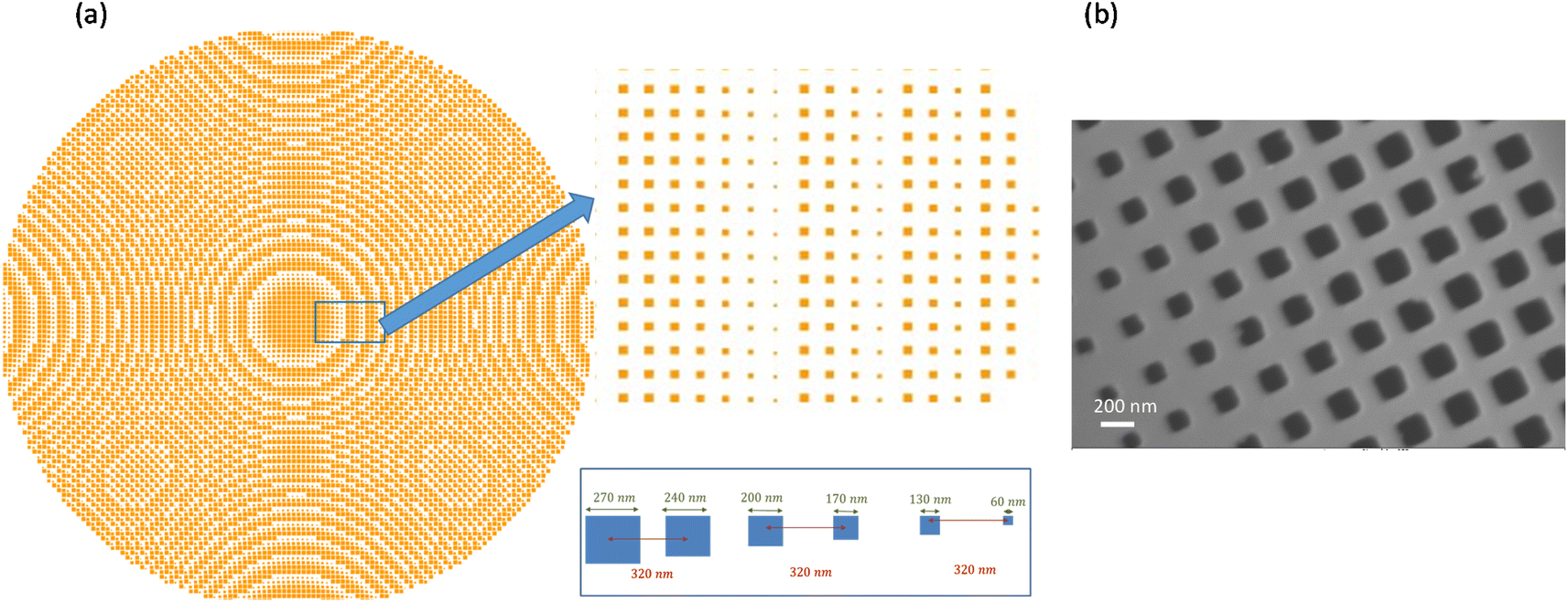 | ||
| Fig. 1 Illustration of the metasurface structure illustrating a special arrangement of square with varying length and (b) scanning electron microscopy (SEM) image of the fabricated NIL master mold with a metasurface pattern on silicon. | ||
2.1 Nano-imprint master mold fabrication
The fabrication process utilized a 4-inch (100) p-type silicon wafer with a resistivity of 5–10 Ω cm and a thickness of 525 μm for the UV-NIL master mold. Nanostructured metasurfaces were created using a combination of E-beam lithography (EBL) and Bosch deep reactive-ion etching (DRIE) methods. To transfer the metasurface patterns onto the wafer, an Ar-6200-0.9 positive tone photoresist and 100 KeV electron beam lithography (JEOL-e-beam writer_nf) were used. Thin Ni films with a 60 nm thickness served as masking layers to facilitate the silicon dry etching process. It's important to note that fabricating the metal masking layer is more complex than using SiO2, requiring three additional processes: metal deposition, reactive ion etching, and chemical etching. The nanoscale structures were constructed using a bottom-up approach, which included metal film evaporation followed by the lift-off procedure.To decide whether Bosch deep reactive ion rtching (DRIE) or cryogenic deep reactive ion etching (DRIE) is better for making optical devices, we must look at the benefits and uses of each method. Bosch DRIE is celebrated for its high speed, affordability, outstanding resolution, and consistency, making it perfect for efficiently crafting complex patterns on silicon bases. This technique has been effectively applied in the creation of high-performance silicon metalenses for optical purposes.36 Conversely, cryogenic DRIE is valued for its meticulous control over profiles and its capability to etch structures with high aspect ratios at lower temperatures. This approach has been instrumental in developing nanostructures and surfaces with exceptional hydrophobic properties through refined etching techniques.37 Additionally, it has played a crucial role in producing silicon nanostructures and trenches with high aspect ratios and controlled profiles. When it comes to making optical devices, Bosch DRIE might be the go-to choice for scenarios where swift production and cost efficiency are key, such as in silicon metalens manufacturing. Meanwhile, cryogenic DRIE might be favored for tasks that demand exact profile control and the creation of nanostructures or features with high aspect ratios. Dirdal, C. A., et al.37 in their study showed that both the Bosch and cryogenic DRIE processes have been successful in achieving high efficiencies in the range of 50–52%. The Bosch process offers the flexibility to achieve different degrees of characteristic sidewall surface roughness, while the cryogenic process produces structures with smooth sidewalls and conforms well to the target dimensions. Both processes have demonstrated their capability of producing high-quality metalenses with close to theoretical optical efficiency.
The selection between Bosch DRIE and cryogenic DRIE for optical device fabrication hinges on the specific outcomes sought from our production process. Cryogenic etching tends to yield patterns with significant surface roughness around the openings, leading to highly irregular opening shapes, whereas Bosch etching results in smoother openings at the top. Because with prolonged etching time, the mask layer can degrade faster due to the drop in temperature of the substrate given our particular application needs, Bosch DRIE emerges as the optimal choice due to its effectiveness and cost efficiency, aligning closely with our project's requirements.
For the silicon etching process, an Oxford Instruments Plasmalab 100 Ltd. inductively coupled plasma reactive ion etching (ICP-RIE) system, equipped with a liquid nitrogen dewar, was used. This setup enabled the DRIE etching process to be conducted at temperatures as low as −20 °C. To assess the effects of various etching parameters on the profile, different variables expected to influence outcomes, such as Bosch DRIE scallop sizes, sidewall tapering, and undercut, were examined across three similar UV-NIL masters.
The etching process was conducted in two main steps. Initially, a polymer layer resistant to etching (C4F8) was deposited across the substrate's surface to safeguard the sidewalls during etching. This step led to the creation of nanoholes with vertical sidewalls in the silicon wafer. Then, the polymer layer at the bottom of these holes was eliminated using ion plasma bombardment, preparing the surface for etchant gas (SF6) interaction with silicon. The introduction of SF6 into the silicon substrate for a brief period marked the final phase of the etching process, with the key process parameters detailed in Table 1.
| Process parameters | |
|---|---|
| Gas flow rate (sccm); etching | SF6: 100 C4F8: 10 |
| Gas flow rate (sccm); deposition | SF6: 10 C4F8: 100 |
| Substrate temperature (°C) | −20 |
| ICP power (W) | 1300 |
| RF power (W) | 5 |
2.2 UV-NIL stamp mold fabrication
Creating the stamp mold involved a detailed, multi-step procedure to ensure precision and quality. The process began with selecting 4-inch glass plates as the base material, which were first thoroughly cleaned using ultrasonic baths in acetone and isopropyl alcohol (IPA), each for 15 minutes. This was followed by drying with nitrogen gas to remove any remaining contaminants. To improve the glass plates' affinity for water—a property known as hydrophilicity—they were treated with plasma for 10 minutes and then heated at 200 °C for half an hour to modify their surface characteristics further.In parallel, the master mold was prepared for the stamping process. It received a coating of an anti-sticking layer, specifically EVGASL1, applied at a high speed to ensure an even layer. To activate this coating, a solution of 3 M Novec 7100 Engineering fluid was applied. The silicon wafer, designated to receive the imprint from the master mold, was preheated to 120 °C for two minutes to make it ready for stamping and then further heated to 150 °C for five minutes to remove any residual moisture.
The material for the stamp itself was then mixed, combining 20 mL of EVG WS material (designed for UV-NIL applications) with 0.5 mL of a photoinitiator to trigger the curing process under UV light. This mixture was stirred and then left to rest to allow any trapped air to escape, ensuring a smooth, bubble-free consistency.
Following this, the glass wafer was coated with an adhesion promoter, EVGPRIM K, and reheated to ensure that the coating firmly adhered to the wafer. The glass was then meticulously aligned and placed on the master mold, and a precise amount of the UV-NIL solution was applied between them, starting from one edge to avoid trapping air in the solution. This assembly was left undisturbed, allowing the solution to evenly spread across the interface due to capillary action.
Finally, the entire setup was exposed to UV light from a mercury vapor lamp for 15 minutes, curing the polymer and solidifying the pattern onto the glass. The system was then left to stabilize at room temperature overnight before the newly formed stamp mold was carefully separated from the master mold. This intricate process ensured the creation of a high-quality stamp mold, ready for use in transferring nano-scale patterns onto substrates.
2.3 UV-NIL metasurface fabrication
Fabricating metasurfaces with UV-NIL is a methodical process, structured into three principal steps. Initially, titanium dioxide (TiO2) is deposited onto a 2-inch sapphire substrate using electron beam evaporation (EBE), creating a foundational layer crucial for the subsequent steps. This process, particularly the deposition and resulting optical properties of the 600 nm TiO2 thin film, is detailed further in our previous work. An illustrative overview of the entire UV-NIL patterning process is provided in Fig. (2).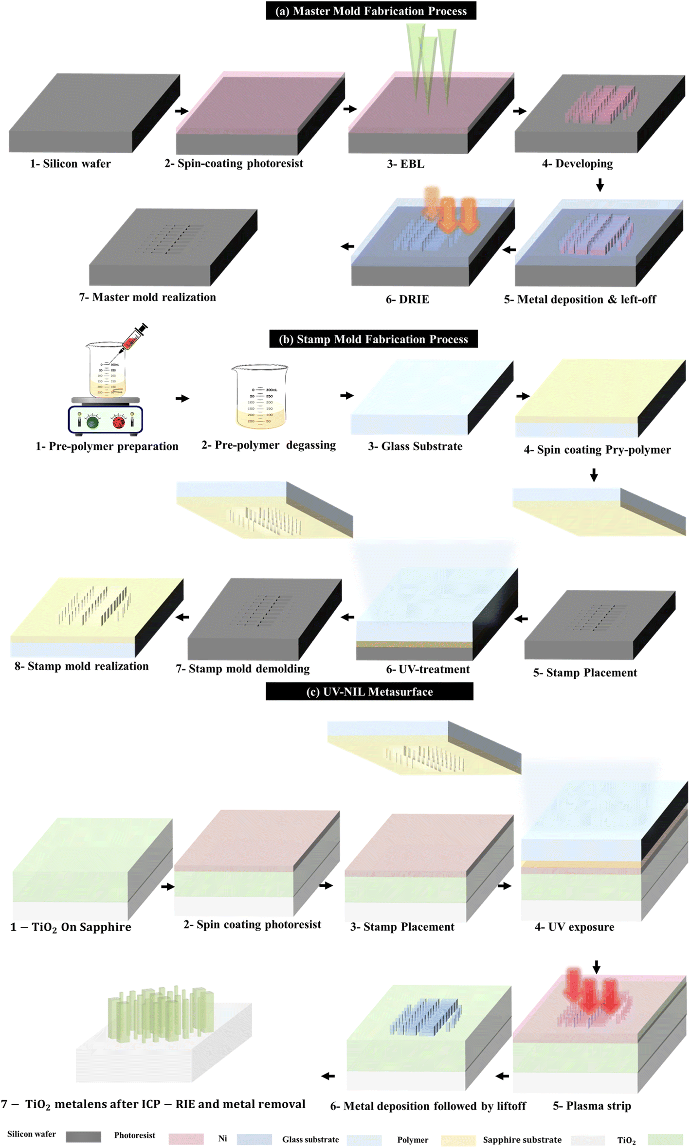 | ||
| Fig. 2 UV-NIL metasurface fabrication process overview. (a) Master fabrication: steps involve (1) silicon wafer cleaning and preparation; (2) spin-coating with a photoresist; (3) electron beam exposure; (4) wafer development; (5) metal deposition and lift-off of the photoresist to transfer the metasurface pattern, followed by (6) silicon Bosch deep reactive ion etching process using SF6 and C4F8, and a final chemical etching step to remove the metal layer completely. So, holes are obtained and (b) stamp fabrication: steps include (1) prepolymer mixture preparation; (2) degassing to remove trapped air; (3) cleaning and preparing the glass substrate; (4) dropping the soft stamp prepolymer mixture; (5) placing the master mold on the stamp mold; (6) UV-curing the stamp material; (7) removing the stamp from the master mold. (c) Metasurface fabrication by UV-NIL involves (1) TiO2 deposition by EBE followed by surface preparation; (2) spin coating with a UV photoresist; (3) aligning the stamp; (4) UV exposure for resist curing; (5) O2 plasma strip to remove unwanted photoresist residuals post-stamp detachment; (6) masking material deposition followed by lift-off; (7) RIE process and chemical removal of the masking layer. | ||
The second phase involves the application of the TiO2 layer onto the sapphire substrate through the UV-NIL process, beginning with a comprehensive cleaning of the wafer using acetone and IPA, each for about ten minutes. This is followed by a brief oxygen plasma treatment for 45 seconds to enhance the surface's hydrophilicity. Afterward, the substrate is treated with the EVGPRIM K adhesion promoter and then heated to 120 °C for two minutes to improve adhesion. A photoresist, specifically an EVG UV-NIL 200 nm from EV Group in St. Florian am Inn, Austria, is then evenly applied at a speed of 3000 rpm for one minute, achieving a desired thickness of 200 nm. The nanoimprint itself is performed using an EVG contact aligner system under vacuum and specified exposure settings. Before exposing to UV light, the substrate is coated with an anti-sticking layer, EVGASL, and then baked at 120 °C for two minutes. The actual UV exposure is carried out at an intensity of 180 mJ cm−2 for 200 seconds, under a vacuum pressure of 950 mbar.
The final step involves etching the thin film, a crucial phase where the remaining photoresist layer, or the residual layer left between the etched patterns, must be meticulously removed. This is achieved through a reactive ion etching (RIE) process at Oxford Instruments Plasma Lab 100 Ltd., Yatton, UK, using specific parameters: a pressure of 30 mTorr, an ICP power of 50 W, and an oxygen flow of 50 sccm, over varying durations to ensure optimal removal. Subsequently, a thin, approximately 30 nm, layer of nickel is deposited using EBE, facilitating the lift-off process of the remaining photoresist with NMP and ethanol over 19 hours and one hour, respectively. The process concludes with the transfer of the metasurface pattern to the TiO2 layer, employing the same ICP-RIE technique described in our earlier publication.
3. Results and discussion
3.1 Master mold fabrication and silicon loading effect
The successful realization of the nano-pattern features of the UV-NIL metasurface is highly dependent on the etching profile of the silicon master mold. Among all techniques of RIE processes, the Bosch DRIE process for silicon that involves repetitive passivation and etching cycles enables the etch process to proceed deeper into the substrate with a small tapping angle.7,9,10 The first step of the etching process is the deposition of an etching-resistant polymer layer (C4F8) over the entire substrate surface. The deposition of the polymer prevents the sidewalls from being etched; thus, nano-holes with vertical sidewalls in the silicon wafer are obtained. Next, the polymer layer on the bottom of the hole is removed by bombarding ion plasma to clear the surface for the etchant gas reactive species to interact with silicon atoms. In the last step of the process, (SF6) is introduced into the silicon substrate for a short time. Then the flow of (C4F8) process gas starts the deposition coating of the passivation polymer before etching further.Understanding the nuances of this process, such as the specific pressures and temperatures used, is vital because of the complex patterns we aim to create. A particular challenge is the 'loading effect,’ where the rate of etching changes based on the size of the openings we're creating. In exploring the optimization of the Bosch (DRIE) process for fabricating nano-pattern features on (UV-NIL) metasurfaces, we scrutinized three distinct sets of process parameters across conditions MM-1, MM-2, and MM-3. Each condition was carefully designed to investigate the impact of etching parameters on the silicon loading effect, crucial for achieving uniform and precise nano-patterns. These adjustments let us closely examine how each parameter affects the depth of the etch, the angle of the walls, and the smoothness of those walls, using focused ion beam scanning electron microscopy (FIB-SEM) for detailed analysis.
The main process parameters are summarized in Table 2. For conditions MM-1 and MM-2, the active time for the etching and passivation steps was consistently set at 8 seconds, emphasizing a standardized approach to the duration of silicon interaction with etching gases. Then, it was reduced to 1 second for condition MM-3 to investigate the effect of process active time on the etching profile.
| Process parameters | MM-1 | MM-2 | MM-3 | ||||
|---|---|---|---|---|---|---|---|
| Etching step | Passivation | Etching | Passivation | Etching | Passivation | Etching | |
| Active time (s) | 8 | 8 | 8 | 8 | 1 | 1 | |
| Pressure (mTorr) | 30 | 35 | 8 | 8 | 7.5 | 7.5 | |
| Total cycles | 10 | 10 | 10 | ||||
However, the conditions diverged significantly in terms of chamber pressure during the etching steps. In MM-1, a pressure of 30 and 35 mTorr for the passivation and the etching processes, respectively, was employed, serving as a baseline for comparison. MM-2 showed a slight decrease in pressure to 8 mTorr for both steps, aiming to assess the effects of elevated pressure on etching uniformity and depth. The most notable departure was observed in MM-3, where pressure was dramatically reduced to 7.5 mTorr. This significant adjustment was hypothesized to enhance etching uniformity by minimizing variations induced by the silicon loading effect, potentially leading to smoother sidewall profiles and more consistent etch depths across the nano-patterned silicon wafer. Each of these conditions maintained a total of 10 cycles of passivation and etching, underscoring a commitment to a thorough and repetitive process aimed at refining the quality of the etched patterns. This rigorous approach highlights the detailed and methodical experimentation with DRIE parameters, with the ultimate goal of identifying optimal settings that mitigate the loading effect, thus ensuring the successful realization of high-quality, uniform nano-patterns essential for advanced metasurface applications.
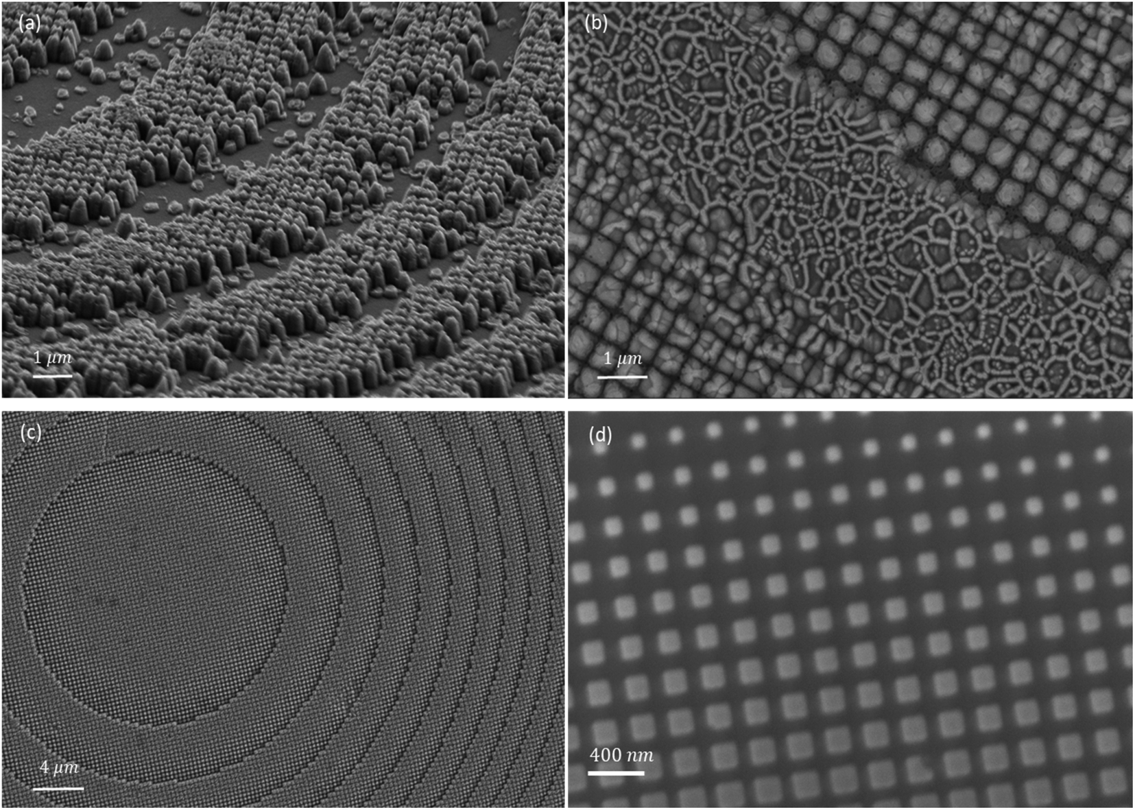
The differences brought about by these adjustments become clear when we look at the SEM images of our metasurface designs, which feature holes ranging from 60 nm to 270 nm in width, see Fig. 3. In the first set of conditions (MM-1), the depth of the etched holes varied widely, demonstrating the pronounced impact of the loading effect, with some holes being as much as 528 nm deeper than others. The second set of conditions (MM-2) showed a significant reduction in this variability, with the maximum difference in hole depth dropping to 212 nm. The third set of adjustments (MM-3) nearly eliminated this disparity, with a minimal difference of just 81 nm between the deepest and shallowest holes.
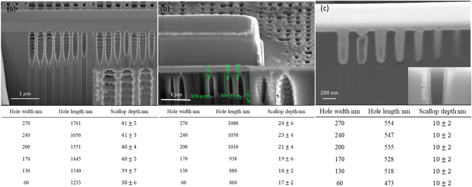 | ||
| Fig. 3 FIB-SEM cross-sectional images of metasurfaces after the Bosch DRIE process; (a) silicon wafer etching profile etched under Bosch DRIE condition MM-1 with different hole widths and Scallop depths. (b) Silicon etching profile with condition MM-2 and (C) with condition MM-3. | ||
These findings not only highlight the critical role of precise control over the DRIE process parameters in creating uniform nano-patterns but also underscore the importance of understanding and mitigating the silicon loading effect. By fine-tuning the cycle duration and pressure for each etching step, we've been able to achieve more consistent etching depths across our metasurface designs, leading to better overall performance and fewer defects in the final product.
3.2 UV-nanoimprint lithography
The UV-NIL process commences with the fabrication of UV-NIL stamps, which are meticulously crafted based on a master mold. These stamps serve as the precise templates for the desired nanoimprint patterns, generated using a glass wafer and a pre-polymer solution. In the stamp manufacturing process, the topographical structure on the master mold assumes a pivotal role, ensuring compatibility with the intended patterning method and material.To assess the impact of the silicon loading effect on the successful creation of stamp molds, atomic force microscopy (AFM) becomes instrumental in characterizing pattern profiles. This investigation yielded three distinct patterns by altering the etching conditions of the master mold, and their corresponding geometric structures are detailed in Fig. 4. It is worth noting that this characterization process maintains the strict criterion of ensuring no contamination in the polymer. The degree of uniformity in pillar heights is denoted by the height differential among the highest and shortest pillars within the crossbar structure. As illustrated in Fig. 4(a)via AFM topography data, a stamp molded in a silicon mold (S_MM-1), as presented in Table 2, exhibits a similar trend in the height profile of the polymer pillars. Specifically, the difference in height between the tallest and shortest pillars measures 200 nm. Notably, this height differential decreases to 110 nm and further to 20 nm for pillars produced in silicon molds (S_MM-2) and (S_MM-3), respectively. Consequently, achieving a stamp mold structure with uniformly consistent pillar heights emerges as a direct consequence of mitigating the silicon loading effect, resulting in enhanced outcomes as this effect is progressively minimized. The examination of polymeric pillar shapes is integral to the actual structural design. The AFM measurements were conducted using a BRUKER RTESPA-300 tip. This tip features a cantilever with dimensions of thickness (T) 3.4 μm, length (L) 125 μm, and width (W) 40 μm, ensuring precision in profiling the nanostructures. The material used for the tip is antimony (n) doped silicon with a resistivity range of 0.01–0.025 Ohm cm, which is known for its high conductivity and durability. The tip itself does not have a front-side coating, which allows for accurate imaging without additional interface layers that could alter the tip–sample interaction. However, the back side of the cantilever is coated with reflective aluminum (Al) to enhance the reflectivity for the laser detection system used in AFM. The tip's cantilever has a resonance frequency (f0) of 300 kHz and a spring constant (K) of 40 N m−1, which are optimal for a balance between sensitivity and stability in measurements.
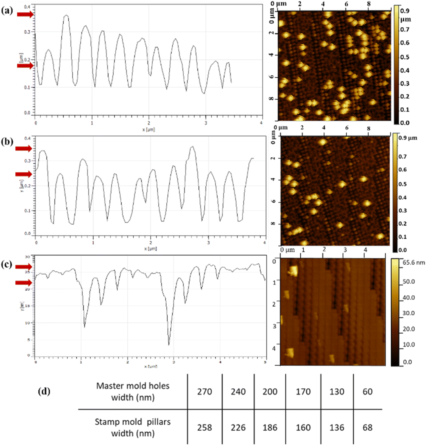 | ||
| Fig. 4 AFM top view images showing a comparison between different geometries after the fabrication of the stamps mold: (a) the right part is a top view for stamp S-MM_1 showing the fully replicated pattern using the master mold (MM-1), and the left part shows the observed height for all pattern pillars. (b) Stamp mold (S-MM-2) with a slightly lower pillar height difference. (c) Stamp mold (S-MM-3) with too little pillar height difference. (d) Comparison summary between the width of the square holes in the master mold (MM-3) and the corresponding pillars of the stamp mold (S-MM-3). | ||
The measurements were conducted on the pillar tops of each stamp due to variations in the results arising from different master molds. Fig. 4(a&b) depict the characteristics of stamps (S_MM-1) and (S_MM-2), revealing cone-shaped tops for all pillars. This outcome is influenced by the geometry of the master molds and its impact on defect patterns, as observed when comparing the fully replicated structures in Fig. 4(a&b) with the hole structures in Fig. 3(a&b). Notably, stamp (S_MM-3) displays fewer defects, featuring relatively flat tops that result in fully patterned areas with sharp square borders.
Additionally, it is essential to note that the stamps are devoid of external impurities or dust, comprising columns of varying lengths where the length discrepancy is visually represented through color contrast. Excess polymers, resultant from the mold separation process, and seals created from silicone molds are observed. Significantly, the mitigation of the silicone loading effect not only standardizes the column lengths but also refines their shapes to more regular and square forms, enhancing the precision and quality of the nanoimprint lithography process. For an independent assessment of pattern geometries, ImageJ software was employed, as evidenced in Fig. 4(c). Fig. 4(d) highlights the nanostructures of the stamp (MM-3), closely resembling the master pattern. Notably, patterns with widths exceeding 100 nm tend to exhibit a square shape, contrasting with smaller structures that assume a rounded form. This rounded shape is contingent on the master pattern, implying that defects originate during the master fabrication process and are influenced by the anisotropic behavior of silicon during the DRIE process.
3.3 UV-NIL metasurface pattering process
The efficacy of nanoimprinting techniques critically hinges on the resist's thickness and uniformity, which facilitate the precise transference of patterns onto substrates. To ensure the integrity of the imprinted patterns, one must judiciously manage the disparity in the heights of the master and the stamp mold pillars. This disparity has profound implications for the residual layer's thickness and the quality of pattern replication, which in turn can either introduce or mitigate imperfections at the interface of the stamp mold and the wafer.Our experimental protocol utilized a uniform resist type—EVG UV-NIL, with a thickness of 200 nm—achieved by spinning at 2000 rpm for a span of 60 seconds. Scanning electron microscope (SEM) images depicted in Fig. 5(a–c) illustrate the outcomes, underscoring the significant role of the silicon loading effect on the UV-NIL procedure. Incomplete metasurface structure transfer was observed with stamps S-MM-1 and S-MM-2, attributed to the pronounced height variance among the polymer pillars. This variance precipitated an unequal depth distribution between the photoresist and substrate, which ultimately defined the residual layer's profile. In contrast, stamp S-MM-3 enabled a full metasurface transfer, which was facilitated by a more uniform distribution of pillar heights, as shown in Fig. 5(c).
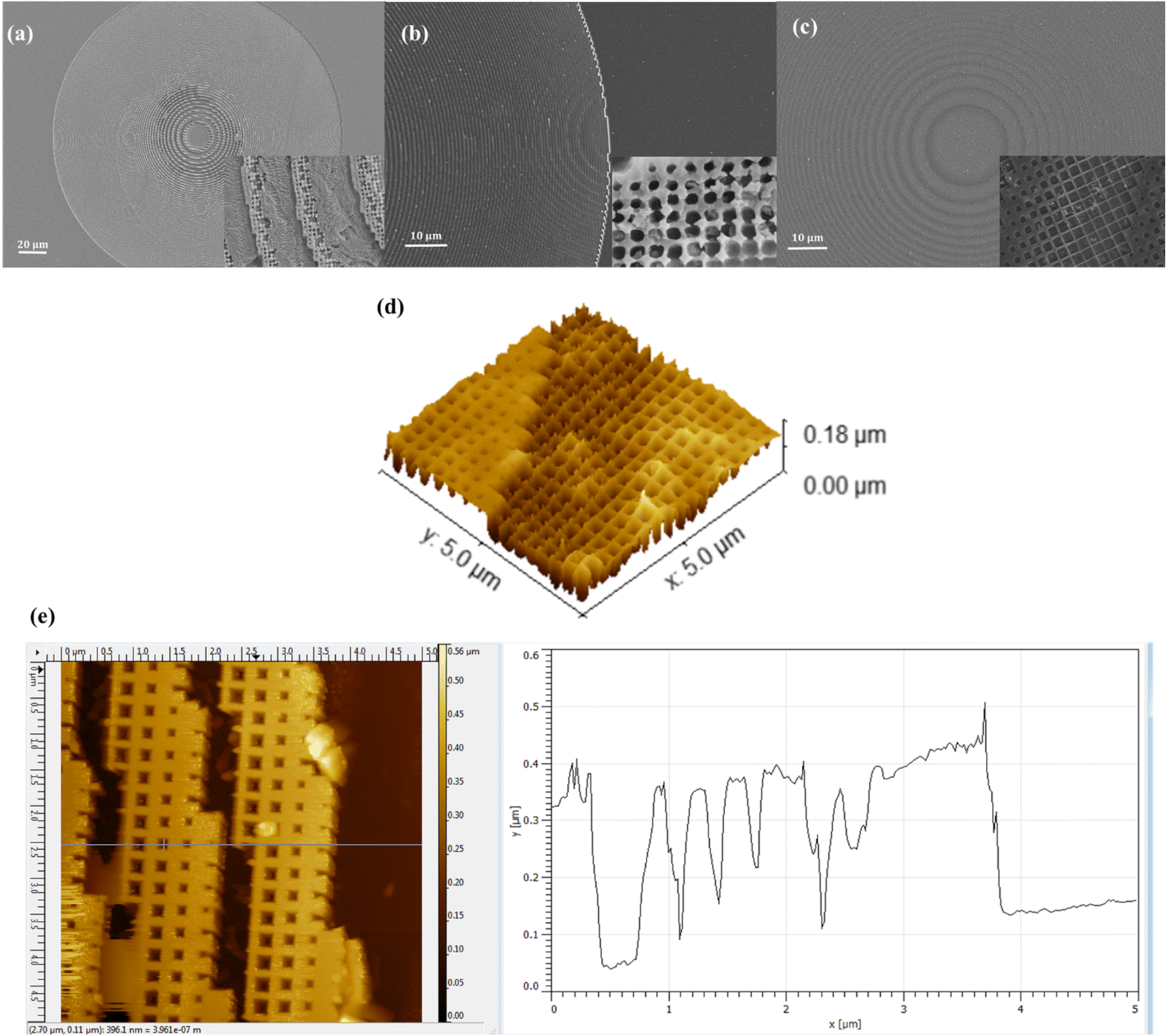 | ||
| Fig. 5 SEM and AFM images demonstrating the metasurface structure transfer via UV-NIL using diverse stamp molds. (a) SEM showing a 200 nm-thick photoresist layer deposited on a TiO2 thin film, patterned utilizing stamp S-MM-1. (b) An SEM image that captured the 200 nm photoresist structure following the NIL process with stamp S-MM-2. (c) SEM illustrating a replicated 2D nanosquare array achieved through NIL with stamp S-MM-3. (d) A 3D AFM image revealing the successful pattern transformation obtained with stamp S-MM-3. (e) AFM that provides a detailed view of the 2D nanosquare array created using stamp MM-3, including a height profile that highlights the topographical contrast within a 5 μm × 5 μm area, showcasing the distinctions between peaks and valleys. | ||
The differential in height between the substrate's surface and the nadirs among the pillars filled with the photoresist is what delineates the residual layer. AFM was performed using a BRUKER RTESPA-300 tip. This tip features a cantilever with dimensions of thickness (T) 3.4 μm, length (L) 125 μm, and width (W) 40 μm, ensuring precision in profiling the nanostructures. The material used for the tip is antimony (n) doped silicon with a resistivity range of 0.01–0.025 Ohm cm, which is known for its high conductivity and durability. The tip itself does not have a front-side coating, which allows for accurate imaging without additional interface layers that could alter the tip–sample interaction. However, the back side of the cantilever is coated with reflective aluminum (Al) to enhance the reflectivity for the laser detection system used in AFM. The tip's cantilever has a resonance frequency (f0) of 300 kHz and a spring constant (K) of 40 N m−1, which are optimal for a balance between sensitivity and stability in measurements.
Fig. 5(d) presents a three-dimensional AFM image capturing the post-UV-NIL patterning process on the photoresist. This image showcases the successful transfer of the pattern onto the substrate, with a pristine surface that is free from dust or foreign contaminants. Despite this cleanliness, there is observable growth within the photoresist. This growth stems from the intrinsic properties of the photoresist being a negative tone, which undergoes a phase transition from liquid to solid upon exposure to ultraviolet light. Such growth becomes apparent when the liquid photoresist, encasing the pillars, solidifies and the pillars are subsequently extracted, revealing the solidified excess.To accurately determine the residual layer's thickness, we strategically scratched away portions of the photoresist to expose the underlying substrate. This deliberate removal was guided by the need to characterize the residual photoresist layer thoroughly. AFM was pivotal in examining the resultant steps, clarifying the delineation between the patterned photoresist and the substrate. Fig. 6(e) showcases this topography, mapped within a thickness range of 12–5 nm. Measurements were specifically taken where the photoresist was absent, ensuring that the data reflected the substrate's surface. Achieving a consistent residual layer is critical, as it underpins the success of the pattern transfer, ensuring that the integrity of the nanoimprinted pattern is preserved across the substrate.
 | ||
| Fig. 6 Top-view SEM images of the metasurface via UV-NIL and ICP-RIE etch processes for the TiO2 thin film after the “photoresist metasurface “structure was dry etched by RIE to remove the photoresist residual layer. (a) Side-view SEM image of the fabricated metasurface after residual layer removal using the RIE process for 20 (sec). (b) Top-view SEM image as a result of photoresist over-etched for 40 (sec). (c) Top-view SEM image of the metasurface after residual layer removal for 30 (sec). (d) Zoom in-view SEM of the nanopatterned metasurface via UV-NIL and RIE methods of the photoresist for 30 (sec). | ||
Therefore, we deduce that the residual layer's uniformity is essential for precise pattern imprinting and can be systematically achieved by regulating the loading effect during the master mold's fabrication. This control is a testament to the intricate yet critical relationship between process parameters and the high-quality transfer of nanoimprint lithography patterns.
3.4 Metasurface fabrication process
Our analysis encompassed a methodical examination at four pivotal stages of the fabrication process: subsequent to the UV-NIL, after RIE to dispel the residual photoresist layer, following the evaporation of Ni, the left-off of the photoresist, and during the inductively coupled plasma reactive ion etching (ICP-RIE) of TiO2.Initially, the UV-NIL imprinting with stamp S-MM-3 was meticulously monitored to ensure that the residual photoresist within the square valleys was completely addressed to avert undercutting the sidewalls of the pattern. The process sought an etch rate of 60 nm min−1 to fully remove the photoresist. The RIE process was conducted at varied times—20, 30, and 40 seconds—to determine the optimal conditions for preserving the integrity of the lithographic pattern, given the non-uniformity of the residual layer's thickness across different patterned areas.
Subsequent to the Ni deposition and the removal of the photoresist, targeted etching of the TiO2 film was imperative. It was discerned from the SEM images in Fig. 6 that even minor inconsistencies in the thickness of the residual layer after RIE could precipitate non-uniform pattern transfers. A successful transfer of the complete pattern was achievable only when the photoresist was etched to a specific degree without being completely removed or over-etched prior to the metal deposition. Fig. 6(a) shows the outcome of an insufficient 20 seconds etch, which led to a non-uniform protective layer and consequent inadequate metal mask deposition, culminating in the formation of truncated cones instead of the intended square TiO2 pillars. Conversely, a 40-second etch time was found to cause the erosion of the square sidewalls, predominantly in regions where the resist barrier was thinner than 60 nm. After Ni deposition and subsequent TiO2 etching, a convergence of these squares was observed, which hindered the formation of distinct square pillars, but allowed for the creation of pillars with altered widths and shapes. Notably, a 30-second etch of the photoresist enabled the replication of the metasurface pattern with no resolution degradation. Fig. 6(c) affirms that proper RIE conditions, particularly the etching duration, were crucial to achieving the design objectives of the metasurface pattern. Such straightforward etching protocols can negate the silicon loading effect and support the creation of nanostructures on a substrate that has been pre-patterned.
A closer inspection of the “UV-NIL metasurface,” fabricated using stamp S-MM-3 and etched for 30 seconds, revealed from a top-down perspective that pillars initially square in form (for sizes less than 150 nm) tended to adopt a rounded shape as shown in Fig. 6(d). This alteration in morphology was linked to the non-uniformity of the stamp surface, a byproduct of depth variations within the master mold's holes. A critical insight from the SEM image analysis highlighted that the shape and dimensions of the TiO2 pillars post-etching hinged significantly on the variability in the stamp pillar heights and were further influenced by the partial or erroneous removal of the photoresist's residual layer.
In the discussion of our results, it becomes evident that the success of the ultraviolet nanoimprint lithography (UV-NIL) and subsequent processes is largely contingent upon meticulous control over the thickness and uniformity of both the photoresist and the residual layers. The use of stamp MM-3 illustrated the critical role of the residual photoresist in preventing undercutting during the reactive ion etching (RIE) phase. Our study found that variations in etch times could yield significantly different outcomes, influencing the fidelity of the lithographic transfer.
The experiments showed that the non-uniformity of the residual layer thickness could lead to a range of complications in pattern transfer fidelity. An insufficient RIE duration resulted in the retention of the residual layer, which subsequently affected the nickel deposition and impeded the formation of the desired TiO2 square pillars. On the other hand, excessive RIE durations led to the over-etching of the photoresist, particularly detrimental for the patterned areas with thinner resist barriers, which caused a loss of the protective layer and, as a consequence, the integrity of the patterned structures.
Our findings underscore the delicate balance required in the RIE process to achieve an ideal metasurface structure. A 30-second etch time was identified as the optimal parameter to replicate the metasurface pattern without resolution loss, demonstrating that precise RIE conditions are paramount for the intended pattern replication. Furthermore, the post-etching analysis of TiO2 pillars with SEM brought to light that the pillars' final shapes are not only a function of the etching process but also a reflection of the stamp's surface homogeneity, which is itself affected by the master mold's conditions.
Thus, while the UV-NIL process and subsequent etching are robust for patterning at the nanoscale, the quality of the master mold, the management of the RIE parameters, and the uniformity of the photoresist layers are all crucial factors that determine the ultimate precision and quality of the nanostructured surfaces. The silicon loading effect, therefore, becomes a critical point of consideration for refining the process and enhancing the outcome of the nanoimprint lithography.
3.5 Optical characterization
Through the process outlined in section 3.4, three metasurfaces were produced and subsequently optically characterized using the setup illustrated in Fig. 7(a). The optical properties of these metasurfaces are determined using the phase function:where λ = 633 nm is the wavelength and r is the radial distance from the centre. The primary function of the metasurface is to concentrate the incident light onto a focal point located at a distance of f = 100 μm from the centre of the lens. This was achieved by introducing the the phase amount ϕ(r) to the incoming beam at each pillar on the metasurface, corresponding to the centre r and the diameter of our metasurface is d = 270 μm.
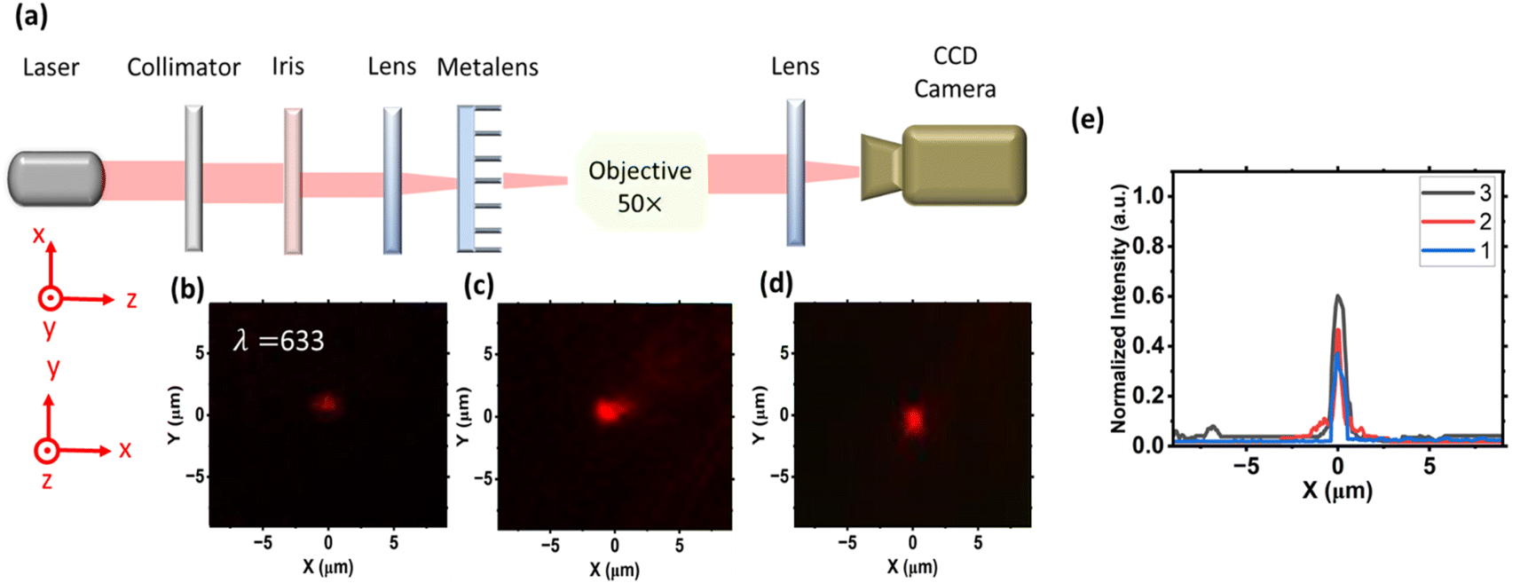 | ||
| Fig. 7 Comprehensive optical characterization of metalenses and their focusing efficiency. (a) Central to the characterization setup is a collimated laser source with a wavelength of 633 nm, ensuring uniform and coherent illumination vital for accurate optical assessment. An adjustable iris meticulously controls the laser beam's diameter to align with the metalens specifications, while an objective lens boasting a numerical aperture of 0.65/40× is paramount in focusing the laser beam to a precise point. The beam, oriented towards the metalens positioned on a kinematic rotation mount, allows for angular adjustments critical for detailed analysis. The metalens-induced focal spots are captured using a CMOS camera, complemented by a lens tube objective, meticulously aligned to gather intricate images of the light focusing phenomena. Mounted on a linear translation stage, this assembly facilitates movement along the z-axis, enabling the capture of the intensity distribution along the axial plane—a key element in evaluating focusing efficiency. This intricate setup underscores the complexity and sophistication necessary in optical experiments aimed at unraveling the subtleties of light manipulation at the nanoscale. (b–d) Images of the laser beam's focal spots as precisely focused using each metalens, with (b) depicting the focal spot by metasurface 1, (c) illustrating metasurface 2, and (d) revealing the focal spot produced by metasurface 3. (e) A plot of the intensity distribution profile associated with the focal spots of the three metasurfaces, providing a visual representation of each metasurface's focusing capabilities and the subtle variations in optical performance across the series. | ||
The three metasurfaces, labeled 1, 2, and 3, underwent the reactive ion etching (RIE) process for the removal of the residual photoresist layer. The duration of the RIE process varied for each metasurface, with metasurface 1 subjected to a 20-second etch, metasurface 2 to a 40-second etch, and metasurface 3 to a 30-second etch. This variation in etching time was strategically conducted to optimize the removal of the residual layer and refine the final outcomes of each metasurface's structural fidelity and optical performance.
The experimental setup illustrated in Fig. 7(a) for characterizing metalenses comprises a series of meticulously arranged components, each serving a distinct function to evaluate the 3D intensity distribution of focused, reflected beams. At the heart of the setup is a collimated laser source emitting light at a wavelength of 633 nm, ensuring the uniform and coherent illumination necessary for precise optical characterization. An adjustable iris controls the beam's diameter to match the metalens's specifications, while an objective lens with a numerical aperture of 0.65/40× plays a critical role in focusing the collimated beam to a fine point. The laser beam is directed towards the metalens mounted on a kinematic rotation mount that facilitates angle adjustments. The focal spots produced by the metalens are captured using a CMOS camera equipped with a lens tube objective, precisely aligned to collect detailed images of the light focusing. This assembly is mounted on a linear translation stage, enabling movement along the z-direction to capture the intensity distribution along the axial plane, essential for assessing focusing efficiency. This elaborate setup, with each component playing a pivotal role, is instrumental in scrutinizing the metalens's performance, highlighting the sophistication required in optical experiments to unveil the nuances of light manipulation at the nanoscale.
To further elucidate the performance of the three metasurfaces under investigation, we plotted the intensity distribution profile in Fig. 7(e). This graphical representation allows for a detailed examination of how light is focused and dispersed by each metasurface, revealing subtle nuances in their optical characteristics.
We scrutinized the full width at half maximum (FWHM) for each metasurface, a parameter of paramount importance, and determined it to be 0.52 μm. The FWHM, defined as the width of the focal spot at half of its maximum intensity, is an essential measure for characterizing the precision with which a lens can focus light. It effectively indicates the sharpness or “tightness” of the focused beam, where a smaller FWHM signifies a more concentrated focal spot. This precision is crucial for applications demanding high resolution and precision, such as imaging, sensing, and laser fabrication.
Interestingly, our characterization revealed that the FWHM remained constant at 0.52 μm across the three metasurfaces, suggesting that the precision in focusing, as determined using the FWHM, remained consistent. However, a notable variation was observed in the intensity of the focused beam among the metasurfaces. This difference in intensity, despite a uniform FWHM, underscores the complexity of optical interactions within metasurfaces and highlights the importance of comprehensive characterization. This suggests that while the ability to concentrate light to a tight focal spot may be consistent, the efficiency with which light is focused—and thus the overall optical efficiency of the metasurfaces—can vary, impacting their suitability for different applications.
4. Conclusion
In this work, we delved into the profound impact of the silicon loading effect, stemming from the deep reactive ion etching (DRIE) of silicon master molds, on the UV-nanoimprint lithography (NIL) patterning of nanofeatures crucial for metalens design aimed at focusing incident laser beams at a specified focal spot. This exploration spanned the intricate stages of UV-NIL for metalens fabrication, examining how the silicon loading effect influences both the master mold's integrity and the subsequent successful removal of the residual photoresist layer. Our findings illustrated the pivotal role of stamp S-MM3, selected for its ability to overcome the challenges that hindered the pattern transfer in stamps S-MM1 and S-MM2, thereby underscoring the necessity for complete yet precise removal of the residual layer to avoid over-etching.Our comprehensive investigation revealed that the silicon loading effect not only affects the master mold but also plays a crucial role in the uniform removal of the residual photoresist layer, a critical step following the UV-NIL process. We employed stamp S-MM3 for the remainder of the fabrication process after identifying that stamps S-MM1 and S-MM2 failed to accurately transfer the metasurface pattern, highlighting the nuanced challenges presented by the silicon loading effect. It became evident that for achieving optimal metasurface fabrication, the residual layer must be meticulously removed without resorting to over-etching, ensuring the fidelity of the transferred pattern.
Through optical measurements, we focused on characterizing the intensity distribution profile of the focal spots associated with the three metasurfaces. Despite the consistent focus on ensuring uniformity in the FWHM, which remained unchanged across all samples, we observed a notable variance in the intensity of the focused beam. This outcome, intriguingly, points to the diffraction-limited nature of these systems where the focal length and FWHM remain constant, yet the intensity of the focused beam varies. This variation underscores the silicon loading effect's selective impact on the intensity of light at the focal spot without altering the focal length or the FWHM, providing valuable insights into the optical characterization and performance assessment of the metasurface.
Conclusively, our study not only advances the understanding of the silicon loading effect on the UV-NIL fabrication of metalenses but also elucidates the complex interplay between process parameters and optical performance. By optimizing the DRIE process and employing strategic measures to ensure the thorough removal of the residual layer, we demonstrate the potential to refine metalens fabrication, thereby enhancing the optical efficiency and performance of these nanoscale devices. Our findings pave the way for further exploration into the design and fabrication of metalenses, promising advancements in optical applications that demand high precision and efficiency.
Data availability
The data presented in this study are available from the corresponding author upon request.Conflicts of interest
The authors declare no conflict of interest.Acknowledgements
This research was funded by KAUST Baseline Fund BAS/1/1664-01-01, GCC Research Council Grant REP/1/3189-01-01, and Competitive Research Grants URF/1/3437-01-01 and URF/1/3771-01-01.References
-
A. Cattoni, et al., Soft UV nanoimprint lithography: a versatile tool for nanostructuration at the 20nm scale, Recent Advances in Nanofabrication Techniques and Applications, 2011, pp. 139–156 Search PubMed
.
- H. Lan and H. Liu, UV-nanoimprint lithography: structure, materials and fabrication of flexible molds, J. Nanosci. Nanotechnol., 2013, 13(5), 3145–3172 CrossRef CAS PubMed
- U. Plachetka,
et al., Wafer scale patterning by soft UV-nanoimprint lithography, Microelectron. Eng., 2004, 73, 167–171 CrossRef
- M. C. Traub, W. Longsine and V. N. Truskett, Advances in nanoimprint lithography, Annu. Rev. Chem. Biomol. Eng., 2016, 7, 583–604 CrossRef PubMed
- M. Neisser, International roadmap for devices and systems lithography roadmap, J. Micro/Nanopatterning, Mater., Metrol., 2021, 20(4), 044601 Search PubMed
-
T. Kohyama, et al., Continued optimization of point-of-use filtration for metal oxide photoresists to reduce defect density, in Advances in Patterning Materials and Processes XL, SPIE, 2023 Search PubMed
- G. Yoon,
et al., Printable nanocomposite metalens for high-contrast near-infrared imaging, ACS Nano, 2021, 15(1), 698–706 CrossRef CAS PubMed
-
H. J. Levinson
The potential of EUV lithography, in 35th European Mask and Lithography Conference (EMLC 2019), SPIE, 2019 Search PubMed
- A. R. Moharana,
et al., Multilayer nanoimprinting to create hierarchical stamp masters for nanoimprinting of optical micro-and nanostructures, Coatings, 2020, 10(3), 301 CrossRef CAS
- M. Nakagawa,
et al., Size-dependent filling behavior of uv-curable di (meth) acrylate resins into carbon-coated anodic aluminum oxide pores of around 20 nm, ACS Appl. Mater. Interfaces, 2016, 8(44), 30628–30634 CrossRef CAS PubMed
- H. Lan,
et al., Mold deformation in soft UV-nanoimprint lithography, Sci. China E, 2009, 52(2), 294–302 CrossRef CAS
- S. Jin,
et al., Scalable nanoshaping of hierarchical metallic patterns with multiplex laser shock imprinting using soft optical disks, Small, 2019, 15(18), 1900481 CrossRef PubMed
- M. Zhang,
et al., UV-nanoimprinting lithography photoresists with no photoinitiator and low polymerization shrinkage, Ind. Eng. Chem. Res., 2020, 59(16), 7564–7574 CrossRef CAS
- M. Okada,
et al., Evaluation of fluorine additive effect on cationic UV-nanoimprint resin, J. Vac. Sci. Technol. B, 2011, 29(6), 06FC04 CrossRef
- S. Donthu,
et al., Facile scheme for fabricating solid-state nanostructures using e-beam lithography and solution precursors, Nano Lett., 2005, 5(9), 1710–1715 CrossRef CAS PubMed
- T. Haatainen,
et al., Nickel stamp fabrication using step & stamp imprint lithography, Microelectron. Eng., 2006, 83(4–9), 948–950 CrossRef CAS
- M. Häffner,
et al., Simple high resolution nanoimprint-lithography, Microelectron. Eng., 2007, 84(5–8), 937–939 CrossRef
- H. Kim,
et al., Fabrication of metallic nano stamp to replicate patterned substrate using electron-beam recording, nanoimprinting, and electroforming, IEEE Trans. Magn., 2009, 45(5), 2304–2307 CAS
- Y. Takano and J. Taniguchi, Fabrication of the grid pattern on a roll mold by electron beam direct writing, Microelectron. Eng., 2018, 193, 41–46 CrossRef CAS
- J. Taniguchi,
et al., 3D Mold Fabrication Techniques Using an Inorganic Resist, Trans. Magn. Soc. Jpn., 2004, 4(4–2), 235–240 CrossRef
- P. Voisin,
et al., High-resolution fused silica mold fabrication for UV-nanoimprint, Microelectron. Eng., 2007, 84(5–8), 916–920 CrossRef CAS
- Z. Peng,
et al., Continuous roller nanoimprinting: next generation lithography, Nanoscale, 2023, 15(27), 11403–11421 RSC
- Y. Lee,
et al., Laser-Assisted Nanotexturing for Flexible Ultrathin Crystalline Si Solar Cells, Sol. RRL, 2023, 7(19), 2300376 CrossRef CAS
- B. Yang, M. Yu and H. Yu, Azopolymer-based nanoimprint lithography: recent developments in methodology and applications, ChemPlusChem, 2020, 85(9), 2166–2176 CrossRef CAS PubMed
- S. Barcelo and Z. Li, Nanoimprint lithography for nanodevice fabrication, Nano Convergence, 2016, 3, 1–9 CrossRef PubMed
- S. Y. Chou, P. R. Krauss and P. J. Renstrom, Nanoimprint lithography, J. Vac. Sci. Technol., B: Microelectron. Nanometer Struct.--Process., Meas., Phenom., 1996, 14(6), 4129–4133 CrossRef CAS
- L. J. Guo, Recent progress in nanoimprint technology and its applications, J. Phys. D: Appl. Phys., 2004, 37(11), R123 CrossRef CAS
- X. Fu,
et al., A rapid thermal nanoimprint apparatus through induction heating of nickel mold, Micromachines, 2019, 10(5), 334 CrossRef PubMed
- P. Cantu, T. L. Andrew and R. Menon, Patterning via optical saturable transitions-fabrication and characterization, J. Vis. Exp., 2014,(94), e52449 Search PubMed
- Z. Gan,
et al., Three-dimensional deep sub-diffraction optical beam lithography with 9 nm feature size, Nat. Commun., 2013, 4(1), 2061 CrossRef PubMed
-
P. Gu, et al., Multi-photon response of photon-number-resolving superconducting single photon detector, in 2015 40th International Conference on Infrared, Millimeter, and Terahertz Waves (IRMMW-THz), IEEE, 2015 Search PubMed
- T. Noguchi,
et al., Photoresponsive Polymer Films with Directly Micropatternable Surfaces Based on the Change in Free Volume by Photo-Crosslinking, Adv. Mater. Interfaces, 2022, 9(9), 2101965 CrossRef CAS
-
S. H. Ahn and L. J. Guo, High-Speed Roll-to-Roll Nanoimprint Lithography on Flexible Plastic Substrates This research is supported by NSF (grant No. CMII 0700718), AFOSR (Grant No. F064-006-0084), and the University of Michigan Technology Transfer Office (GAP Fund). We Thank Dr Jin-Sung Kim for Providing the Short-Period Si Mold Used in This Study, 2008 Search PubMed
- J. Yeom,
et al., Maximum achievable aspect ratio in deep reactive ion etching of silicon due to aspect ratio dependent transport and the microloading effect, J. Vac. Sci. Technol., B: Microelectron. Nanometer Struct.--Process., Meas., Phenom., 2005, 23(6), 2319–2329 CrossRef CAS
- Z. Alnakhli,
et al., Reflective metalens with an enhanced off-axis focusing performance, Opt. Express, 2022, 30(19), 34117–34128 CrossRef CAS PubMed
- A. M. Baracu,
et al., Silicon metalens fabrication from electron beam to uv-nanoimprint lithography, Nanomaterials, 2021, 11(9), 2329 CrossRef CAS PubMed
- C. A. Dirdal,
et al., UV-nanoimprint and deep reactive ion etching of high efficiency silicon metalenses: High throughput at low cost with excellent resolution and repeatability, Nanomaterials, 2023, 13(3), 436 CrossRef CAS PubMed
| This journal is © The Royal Society of Chemistry 2024 |