
A sustainable approach to large area transfer of graphene and recycling of the copper substrate†
Michael Cai
Wang
 *a,
Widianto P.
Moestopo
a,
Satoshi
Takekuma
b,
Shama Farabi
Barna
a,
Richard T.
Haasch
c and
SungWoo
Nam
*ab
*a,
Widianto P.
Moestopo
a,
Satoshi
Takekuma
b,
Shama Farabi
Barna
a,
Richard T.
Haasch
c and
SungWoo
Nam
*ab
aDepartment of Mechanical Science and Engineering, University of Illinois at Urbana – Champaign, Urbana, Illinois 61801, USA. E-mail: cwang99@illinois.edu; swnam@illinois.edu
bDepartment of Materials Science and Engineering, University of Illinois at Urbana – Champaign, Urbana, Illinois 61801, USA
cFrederick Seitz Materials Research Laboratory, University of Illinois at Urbana – Champaign, Urbana, Illinois 61801, USA
First published on 3rd August 2017
Abstract
Graphene, the prototypical two-dimensional material, has been a subject of much interest and extensive studies in the past few decades. Carbon dioxide, on the other hand, has gained infamy because of global climate change concerns. In this Communication, we demonstrate an unlikely but useful marriage between these two ostensibly juxtaposing carbon-containing compounds. Specifically, we address the challenges in sustainable graphene manufacturing by developing a new route for graphene transfer and reuse of the copper catalyst substrate via carbonic acid enabled electrochemical under-etching delamination. Electrochemical reduction of the cuprous oxide (Cu2O) interlayer between the copper catalyst substrate and the chemical vapour deposition (CVD) synthesized surface layer graphene is achieved by using carbon dioxide as the precursor for making a conductive carbonic acid electrolyte. This under-etching delamination approach to graphene transfer mitigates the conventional need for harsh chemical etchants that otherwise expend the copper catalyst. This approach also removes the need for the concomitant multiple subsequent rinsing steps typically needed for chemical etching or delamination via salt/alkali based electrolytes, thereby significantly reducing the process water usage. In addition, we also show the application of using food-grade ethyl cellulose as the thin film handle layer for the transfer process. This inexpensive and environmentally benign alternative for the polymeric thin film replaces the conventionally used high grade polymers that are typically solvated in harsh solvents. We expect our development to enable more environmentally sustainable and cost-effective strategies for the large-scale integration of graphene and analogous 2D materials and their devices, and also to generate new application streams for value-added uses of industrially captured carbon dioxide.
Introduction
As graphene and the ever growing family of two-dimensional (2D) materials move from the laboratory to large scale and high volume applications and production, there exists a critical need to improve their yield and manufacturability.1 Aside from the synthesis quality and intrinsic crystallinity of 2D materials, the material properties and the final device performance of such atomically thin materials are especially susceptible to cracks, voids, wrinkles and residues from polymer handle layers and etchant solutions. While there have been many techniques developed to synthesize and transfer the most prototypical and prolific 2D material, graphene, they almost all involve some use of harsh chemical etchants or strong organic solvents and require expenditure of the high-purity metal catalyst.2,3 In particular, recent progress on the synthesis of large grain, epitaxial graphene on relatively expensive single crystal Cu(111) substrates urgently necessitates the conception of an efficient and clean method to reuse the high-purity copper growth substrate.4 An established technique to completely transfer and reuse the synthesis substrate is through electrochemical delamination.The earliest works on delamination transfer of graphene were based on electrolysis induced hydrogen bubble delamination of poly(methyl methacrylate) (PMMA) supported graphene from the copper or platinum growth substrate used as the cathode.5,6 These and many other subsequent works all function on the basis of electrolysis-induced bubble generation at the cathode (i.e. underneath the delaminated or delaminating graphene) in the presence of a conductive aqueous electrolyte (ionic solution) or bubble generation as a result of chemical etching.7–14 While the bubbles assist with accelerating the delamination rate, they tend to damage the graphene during the delamination process and also the bubbles are trapped underneath the graphene upon transfer (Fig. S1, ESI†), ultimately preventing conformal contact and complete coverage.
One interesting strategy to mitigate cathode bubbling induced graphene degradation is to forego hydrolysis for electrochemical etching of the cuprous oxide (Cu2O) under-layer that forms underneath the graphene.15 While these delamination schemes are simple and prototypical of electrochemical set-ups, there remain challenges in terms of the need to completely remove the ionic contaminants due to the electrolyte residue. In addition, their requirement for a referenced three-terminal electrochemical arrangement increases their cost and complexity beyond the capabilities of many laboratory and manufacturing settings.
To rectify these aforementioned barriers to the large scale manufacturability of high-quality graphene, we propose a green chemistry route. Here we introduce an improved technique based on two-terminal under-etching electrochemical delamination that uses only weak carbonic acid as the electrolyte, inspired by the “bubble-free” delamination technique developed by Cherian et al.15 The use of carbonic acid, which simply evaporates as water and carbon dioxide during the drying process after delamination, simplifies the transfer process into a single step compared with previous methods using salt or alkali based electrolytes such as NaCl or NaOH. The use of these conventional electrolytes necessitates repeated rinsing and the associated dwell time to dilute the chemical residue from the underside of the graphene that is in contact with the electrolyte solution. Oftentimes, the complete removal of the chemical residue might not be possible. In using carbonic acid, on the other hand, the equilibrium reaction allows the carbon dioxide to simply evaporate away with the water as the handle layer/graphene stack dries down and adheres to the target substrate.
Experimental
Materials
Graphene was synthesized via low-pressure chemical vapour deposition (CVD; Rocky Mountain Vacuum Tech Inc.) on a 25 μm thick 99.8% purity copper foil (Alfa Aesar). During the CVD process, the copper foil is ramped to 1050 °C within 45 min and then held at 1050 °C for 1 hour of annealing under hydrogen. The synthesis step takes 2 min where a 2![[thin space (1/6-em)]](https://www.rsc.org/images/entities/char_2009.gif) :1 ratio of methane and hydrogen is introduced. After the synthesis, the sample is left to cool slowly to room temperature inside the chamber under an argon flush. The details of the synthesis process were published previously.16
:1 ratio of methane and hydrogen is introduced. After the synthesis, the sample is left to cool slowly to room temperature inside the chamber under an argon flush. The details of the synthesis process were published previously.16
Carbonic acid was made via introducing carbon dioxide to fresh deionized (DI) water inside of a consumer-grade soda maker bottle (SodaStream). The source of the CO2 was either via compressed CO2 gas (as per the manufacturer’s recommended soda making procedure) or by simply adding fresh dry ice pellets (Continental Carbonic Products) into the bottle rinsed and then filled with DI water. The conductivities of the solutions were measured using a handheld conductivity meter (HM Digital).
Delamination and transfer procedure
To assist in delaminating the graphene from the copper surface via under-etching the Cu2O layer (Fig. S2 and S3, ESI†), we first subjected the as-synthesized graphene sample to a humidified environment (e.g., sealed inside a plastic bag with wet cleanroom wipes) to induce rapid oxidation of the copper substrate. The graphene samples were then coated with an ethyl cellulose (EC) (Sigma-Aldrich) handle layer film. A solution recipe of 2 wt% EC (46% ethoxyl content, standard 100000 cps for 5% in 80/20 toluene–ethanol blend) solvated only in ethanol was spun-coated at 500 rpm for 90 s. To prevent the unwanted backside graphene from contaminating the solution during transfer, the underside of the sample is subjected to 30 s of oxygen plasma to remove the backside graphene.
Two-terminal electrochemical delamination was conducted either inside an open beaker or in a custom-made vessel filled with freshly prepared carbonated deionized water. Electrical contact between the copper foil and the negative terminal of the DC power supply (Circuit Specialists) is established by both mechanical contact and by attaching double-sided Kapton tape to a strip of copper connected to the DC source. The foil is biased at ∼10 V relative to a platinum electrode placed ∼10 mm away. To initiate the under-etching process, it is advantageous to remove the spin-coated edge beads by trimming the leading edge and side edges of the sample to expose a clean interface where the solution can access the Cu2O layer.
The sample is lowered at a 45° angle into the carbonic acid solution and then progressively submerged further as the delamination process progresses (∼3 min mm−1). We chose the delamination angle to be at 45° so as to mitigate excessive bending of the EC/graphene layer at the delamination front, while providing a steep enough angle from the horizontal to easily visually monitor the delamination of the nearly transparent film from the periphery. Shallower angles (more horizontal) can also be utilized, as it would provide sufficient buoyancy for the graphene/EC stack to float. However, shallower angles would make it more difficult to visualize regions of the sample that have been delaminated as the delaminated film would be very close to the copper substrate. In addition, from our experience, angles greater than ∼60° tended to result in the sample breaking the surface tension of the solution and the entire EC/graphene/copper stack becoming submerged into the solution, thus preventing graphene delamination when the sample is too vertical.
After the EC/graphene stack has fully delaminated from the graphene, the sample is either left idle in the solution as the carbonated solution is no longer effervescent or is picked up with a clean glass slide and then placed back into the solution to remove any large CO2 bubbles. Finally, the EC/graphene stack is transferred onto a clean 285 nm SiO2/Si wafer and left to dry. After the film has adhered to the wafer, it is placed inside a 100 °C oven for 10 min to improve adhesion and to drive off interstitial water. Finally, the sample is rinsed in a covered warm ethanol bath (∼50 °C for 2 minutes) to remove the EC handle layer and then immediately dried under dry nitrogen.
Samples transferred via conventional chemical etching of the copper foil and also NaCl delamination were prepared via CVD synthesis and spin-coated with an EC handle layer in the same manner. The chemically etched samples were floated on top of a saturated sodium persulphate solution until the copper foil substrate is completely removed. NaCl (0.1 M in DI) delaminations were performed in the same manner as with carbonic acid delamination. Both chemically etched and NaCl delamination samples were transferred successively onto five baths of DI water (∼20 min dwell time for each rinse) to remove the chemical residue. The EC layers for the chemically etched and NaCl delaminated samples are removed in the same manner as CO2 delamination.
The custom-built delamination vessel was fabricated from a combination of purchased and 3D printed parts (Fig. 1a and Fig. S4, ESI†). The copper foil is attached onto an angled platform, which travels vertically on a plastic rail. A magnet is installed to a 3D printed carriage attachment where the platform sits, which allows the vertical actuation of the platform using another magnet from outside the vessel. The rail is attached onto the stainless steel sealing plate via two custom-made plastic parts: one secured to the plate and the other to the rail to ease servicing and disassembly. A pressure-tight cord grip is attached through the plate to allow pass-through of the electrical wires. The sealing plate and a silicone seal are fixed to the vessel top using a screw-on collar. The body of the vessel itself is a typical, commercially available 64 oz. wide-mouth canning jar.
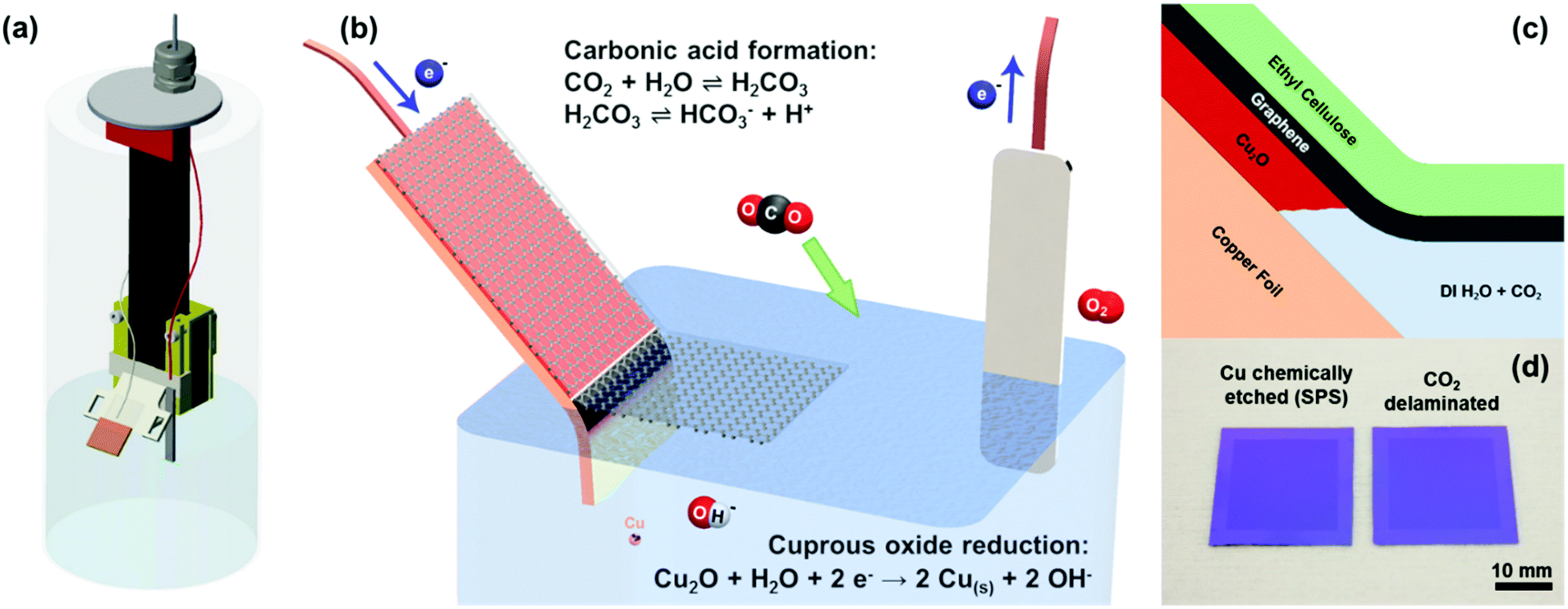 | ||
| Fig. 1 Schematic diagram and mechanism of cuprous oxide under-etch delamination of graphene in carbonic acid solution. (a) Self-pressurized vessel containing the vertical mechanism for (b) the gradual immersion and delamination of ethyl cellulose coated graphene on copper foil into a carbonic acid solution. The copper foil substrate cathode is biased at ∼10 V in a two-terminal DC set-up to allow (c) under-etching of the cuprous oxide interlayer between graphene and the copper foil. (d) This set-up is capable of transferring inch-scale graphene without the use of any chemical etchants such as sodium persulphate (SPS) nor does the sample require subsequent rinsing in DI water. | ||
Material characterization
Raman spectra were obtained with a 532 nm laser using a Nanophoton Raman-11 instrument with a 600 grooves per mm grating. To obtain area-averaged spectra (and to verify material uniformity), the line scan xy_imaging mode was used with a 100×, 0.9NA objective lens to average over 25 × 25 μm regions.To characterize the amount of residual elements for each transfer technique, X-ray photoelectron spectroscopy (XPS) measurements were performed using a Kratos Axis Ultra X-ray photoelectron spectrometer (Kratos Analytical, Inc., Manchester, UK) with monochromatic Al Ka radiation (1486.6 eV). Survey spectra were recorded using a pass energy of 160 eV and high-resolution spectra using a pass energy of 40 eV at a take-off angle of 90° from a 0.7 mm × 0.3 mm area using the hybrid (electrostatic and magnetic immersion) lens mode. Fresh samples were prepared and preserved in isopropanol before XPS measurements by affixing onto the sample holder using double-sided copper tape. The binding energy scale was referenced to the C 1s signal at 284.5 eV, which originates from the graphene and also adventitious carbons (Fig. S5, ESI†). The pressure during analysis was ca. 7 × 10⁻⁷ Pa.
Atomic force microscopy (AFM) topography images were obtained in tapping mode on an Asylum MFP-3D using TAP300AL-G tips (Budget Sensors). The copper foil roughness was extracted based on sampling four arbitrary regions on each copper foil each of 8100 μm2 in planar area. The images were post-processed by first-order flattening, and the root mean square (RMS) roughness values were calculated using Igor.
Results and discussion
Inch scale electrochemical delamination transfer of the as-grown graphene on copper foil was realized via (1) carbonic acid as the conductive electrolyte, (2) Cu2O as the sacrificial under etch layer, and (3) an ethyl cellulose transfer handle layer (Fig. 1b and c). We opted for such an under-etching delamination scheme as opposed to the well-documented bubbling delamination techniques reported by numerous groups due to the higher yield and less damage as compared to bubble delaminated graphene.15 The suppression of bubbling reduces pore formation and fracture during the delamination process and also subsequent drying on the substrate. In this study, standard 25 μm polycrystalline copper foils were used for graphene synthesis. However, this under-etching technique can be easily extended to any of the copper- or oxide-forming substrates. Due to the expense of high-purity copper and monocrystalline Cu(111) substrates, which have been shown to yield high-quality large grains of epitaxial graphene, this technique will prove useful in the reuse of these substrates as well.To impart conductivity into the solution, we rely on the equilibrium between CO2 and water hydration to form carbonic acid with a hydration constant of about 1.7 × 10−3.17–19 While it is a diprotic acid, the bicarbonate formation dominates over the carbonate formation by about three orders of magnitude (dissociation constants of 2.5 × 10⁻⁴ and 4.47 × 10⁻⁷ for bicarbonate and carbonate formation, respectively), resulting in the bicarbonate being the majority anion in the carbonic acid solution. The dissociation of bicarbonate (HCO3−) and hydronium (H+) imparts conductivity to the otherwise highly resistive DI water and allows the electrochemical reduction and under-etching of the Cu2O layer to occur (Fig. 1b and c). While the carbonic acid solution is not as conductive as other conventionally used salt and alkali electrolytes, its main advantage lies in being able to readily evaporate away as water and carbon dioxide subsequent to graphene transfer and drying on a target substrate, leaving a completely clean interface.
To characterize the increase in solution conductivity due to carbonation, we performed several controlled measurements (Table S1, ESI†). While fresh DI water exhibited a conductivity of only 0.1 μs, the addition of compressed CO2 gas (using soda maker) and dry ice pellets (added directly to fresh DI water in the bottle) increased the conductivity to 72.8 μs and 71.9 μs respectively. To gauge the contribution of the conductivity due to the addition of CO2 compared with the incorporation of ambient CO2 (∼0.04%), we agitated fresh DI water by repeatedly shaking vigorously and then letting fresh air into the bottle (∼20 times). By this method of incorporating ambient CO2 into the solution the conductivity of DI water only increased from 0.1 μs to 0.7 μs. These controlled experiments demonstrated the importance of additional CO2 to impart conductivity into the carbonic acid solution, which is significantly higher than that of the incorporation of atmospheric CO2 alone.
Since the delamination process occurs over several minutes, it is important to gauge the level of conductivity changes in the carbonic acid over time and during delamination, we performed several additional controlled experiments. In particular, repeatedly shaking the bottle and venting the pressure (∼20 times) lowered the conductivity to 20.9 μs from 71.9 μs. With the addition of 10 minutes of sonication, the conductivity decreased further to 19.8 μs. However, when left undisturbed (with the bottle cap opened) for 48 hours, the conductivity only dropped to 33.6 μs. As corroborated with successful delamination experiments using carbonated solutions that were left out for several hours, the relative stability of the solution conductivity allows for electrochemical delamination over a long period of time without having to replenish the solution. These conductivity measurements are tabulated in Table S1 (ESI†).
In addition to the specific detachment and transfer process of graphene from the growth substrate to target substrates, the selection of an appropriate and sacrificial handle layer is also critical to the final material quality and device performance.20 This role has conventionally been served by high-grade polymers and photoresists such as PMMA, poly(bisphenol A carbonate) (PC), SU-8, thermal release tape, etc. While these specialized polymers have performed well in a research and development setting, their relatively high cost and their form factor being dispersed in volatile aromatic and ketone solvents such as chlorobenzene, chloroform, anisole, etc. present environmental emissions, workplace health, and material-handling complications.
To find a more sustainable option for the graphene handle layer, we used 2 wt% ethyl cellulose (a common polymer used in food additives and packaging, etc.) in ethanol as the spin-coat solution. We found that an optimal film thickness (∼700 nm) was achieved for 2 wt% EC in ethanol spun coated at 500 rpm for 90 s. Very thin EC films (and also PMMA) failed to have enough mechanical integrity to allow a cohesive film of the handle layer adhered with the graphene to delaminate and did not provide a sufficient pulling force due to surface tension to progress the delamination front. However, too thick a handle layer film also tends to prevent conformal contact to the target substrate and subsequent large-area transfer.
This EC handle layer film recipe ensures that the film is robust enough for experimental handling and bending during the delamination process. It also ensures that the film is thick enough to be impermeable to fracture against the occasional bubbles that form on the underside of the graphene due to CO2 off gassing. Simultaneously, the film is thin enough to be conformal to the target substrate after drying. Thinner EC films failed to initiate delamination, while thicker EC films tended to not allow graphene to properly adhere to the SiO2 substrate after drying. In addition to the cost and environmental advantages, the use of EC as an ethanol soluble polymer handle layer also makes this process compatible for transfer onto a variety of soft or polymeric substrates that would otherwise not tolerate many types of commonly used solvents (acetone, anisole, chlorobenzene, etc.).21–25
The electrochemical under-etching delaminations of graphene were performed in a two-electrode set-up using carbonic acid as the electrolyte. By biasing the graphene/Cu2O/copper foil stack with a negative voltage relative to the platinum counter electrode, the Cu2O layer between the graphene and copper foil is electrochemically reduced to metallic copper (Fig. 1b and 1c).26
| Cu2O + H2O + 2e− → Cu + 2OH− |
| 2H2O → O2 + 4H+ + 4e− |
To confirm the successful transfer of graphene onto the SiO2 substrate (Fig. 1d), we performed optical microscopy, scanning electron microscopy (SEM), and Raman spectroscopy. Bright field images (Fig. 2a and b) showed the same level of metrology between graphene derived from carbonic acid delamination and chemically etching the copper, with negligible voids and defects, including at the graphene grain boundaries. From the SEM (Fig. 2c), it can be seen that the small size bilayer islands formed during CVD transferred monolithically with the monolayer regions and grain boundaries without any obvious defects. The Raman spectra (Fig. 2d) averaged over 25 μm2 show a 2D/G ratio of ∼2, suggesting predominantly monolayer graphene, and a negligible amount of defects (D peak).27 The three different Raman spectra between chemically etched copper, 0.1 M NaCl delamination, and carbonic acid all showed similar spectral features and peak intensities.
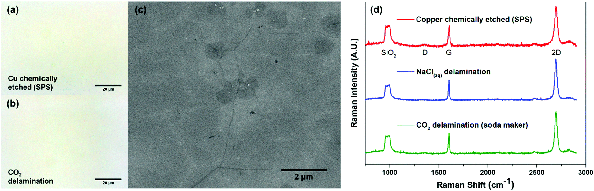 | ||
| Fig. 2 Optical microscopy, SEM and Raman spectroscopy characterization and comparison between chemical etching and delamination transferred graphene. Optical microscopy images of (a) large area chemical etching (sodium persulphate) transferred and (b) carbonic acid delamination transferred graphene on the SiO2 substrate, both showing negligible voids and defects. (c) SEM image of carbonic acid delamination transferred graphene on the SiO2 substrate showing that under-etching delamination is independent of the graphene film thickness and allows for monolayer regions with bilayer islands to be transferred monolithically. (d) Raman spectra of graphene transferred using different techniques (chemically etched (red), NaCl solution delaminated (blue), carbonic acid delaminated (green)) showing the absence of any D peak and demonstrating good monolayer thickness uniformity from the area-averaged 2D/G peak ratio of ∼2. | ||
To further confirm the presence of graphene and also to assess the level of contamination between the various processes, we conducted XPS analysis of the as-transferred sample on 285 nm SiO2/Si substrates. As expected, all of the samples (chemically etched via sodium persulphate, bubble delamination in 0.1 M NaCl, and CO2 delamination) showed characteristic carbon peaks around 285 eV (Fig. S5, ESI†) from the monolayer graphene as well as adventitious carbon. All of the samples showed the absence of a copper signature in the XPS survey scans (Fig. 3a), suggesting complete delamination and detachment from the copper substrate. The surveys also lack any characteristic peaks due to iron or chlorine, elements that are associated with conventional copper etchants for graphene transfer such as ammonium persulfate, sodium persulphate, ferric chloride, or hydrochloric acid.28
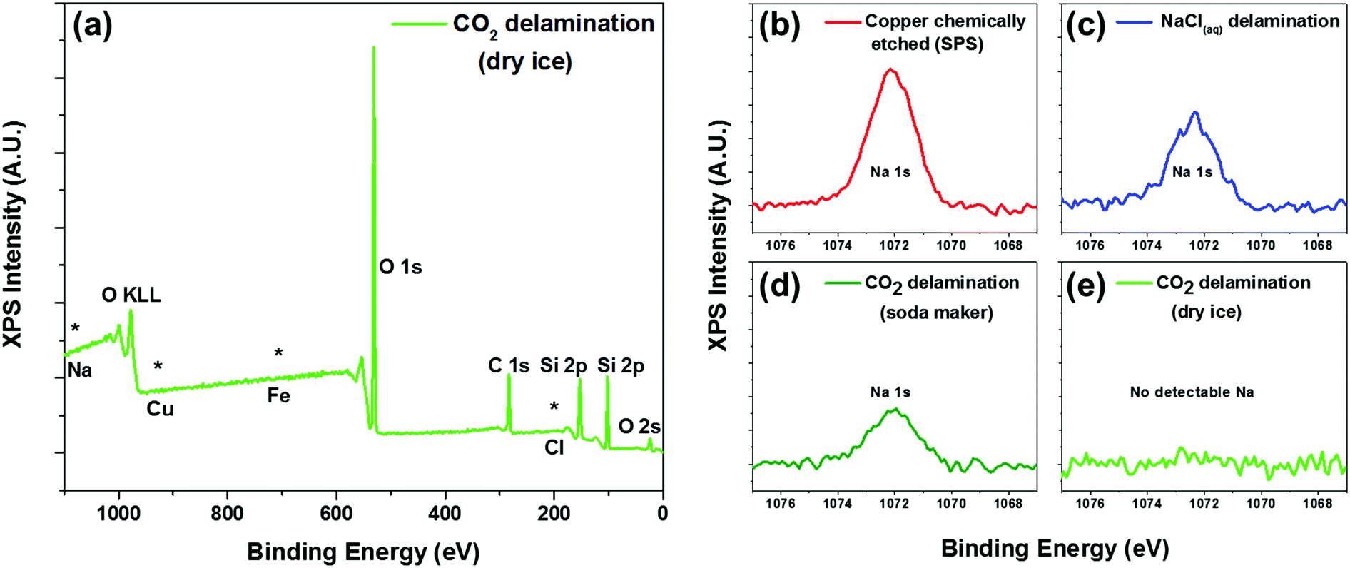 | ||
| Fig. 3 XPS characterization of contaminants. (a) XPS survey of CO2 delamination (from dry ice) showing the absence of signatures from sodium, copper, iron, chlorine, or sulphur species associated with conventional chemical etching techniques. High resolution XPS spectra (b–e) indicating the presence of sodium contamination in (b) chemically etched (sodium persulphate), (c) NaCl electrolyte delaminated, and also (d) CO2 delaminated samples using compressed CO2 from the soda maker. (e) Delaminations done using carbonic acid generated from dry ice pellets did not show any sodium residue in the XPS spectra. | ||
Interestingly, only the dry ice derived carbonic acid delamination showed an absence of sodium in the XPS spectra. In spite of the repeated rinsing in DI water subsequent to chemically etching the copper foil or delamination using a 0.1 M NaCl solution, we still found the presence of sodium in the XPS spectra (Fig. 3b and c). Incidentally, we also found that regardless of the well-controlled processing condition and the handle layer used, there was always the presence of sodium for graphene delaminated using carbonic acid derived from the commercially available gas canister. Conversely, the samples that were delaminated with carbonic acid derived from dry ice pellets did not yield any sodium residue detectable in the XPS (Fig. 3d).
Thereafter, we have transitioned to solely using dry ice pellets due to concerns about this aforementioned sodium contamination and also due to its relatively lower cost. For an approximate comparison, the gas canister costs $15 per refill at retailers that is enough to make 60 litres of carbonated DI water, whereas each litre of DI water requires only about ∼20 g of dry ice (at ∼$2 per kg). A more ideal configuration of in-situ bubbling dry CO2 is currently being developed to afford the convenience of using pressurized CO2 gas (as opposed to dry ice) while mitigating sodium contamination from these consumer product sources.
One of the most important aspects of graphene delamination is to reuse the copper catalyst substrate for repeated synthesis. After the EC/graphene stack has completely been delaminated from the copper foil, the surface is cleaned for the next iteration of synthesis and delamination. Once the copper foil surface has been completely reduced (i.e. only metallic copper remains on the surface after delamination), it is cleaned in a warm ethanol bath. Finally, 30 s of oxygen plasma is applied to remove any remaining adsorbates or other polymeric contaminants during the rinsing process and to prepare the surface for the next CVD process. The subsequent graphene CVD processes are the same for every iteration of delamination and synthesis.
For each iteration of CVD synthesis and delamination, we verified the graphene quality with Raman spectroscopy and also characterized the morphological changes to the copper substrate (Fig. 4). Due to the repeated annealing at high temperatures during CVD synthesis, subsequent surface oxidation to cuprous oxide, and reduction thereof, the surface becomes progressively smoother (from 181.56 nm to 58.89 nm after three cycles) (Fig. 4a, b and Fig. S6, ESI†). In addition to the progressive smoothing of the machining striations on the copper foil during the vendor manufacturing process, the graphene quality remained constant with each iteration as with the initial growth as confirmed by Raman spectroscopy (Fig. 4c). This demonstrates the capability to repeatedly reuse the copper foil substrate for successive re-synthesis and delamination transfer of graphene while maintaining the same level of material quality and operating conditions.
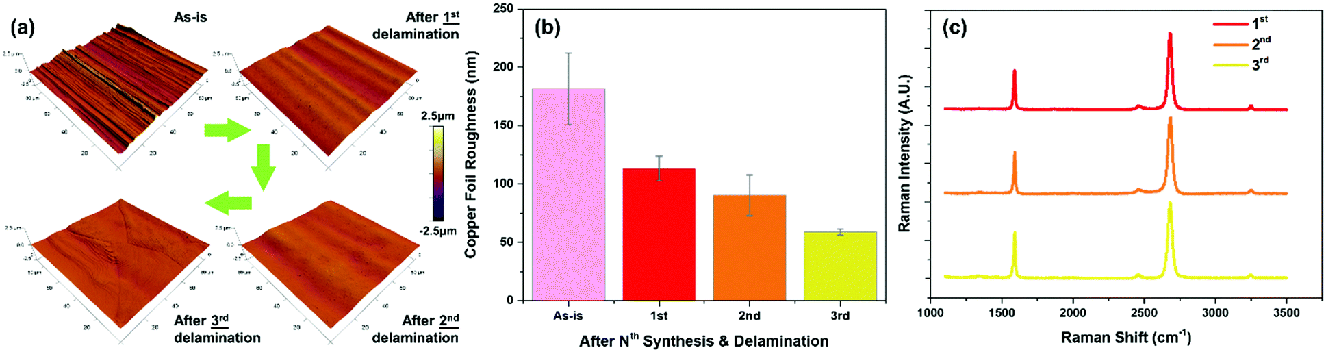 | ||
| Fig. 4 Iterative delamination and re-synthesis of graphene. (a) AFM topography images of the surface of the copper catalyst after successive graphene synthesis and delamination steps up to the third synthesis and delamination. (b) The roughness of the copper surface progressively becomes smoother with more synthesis and delamination steps. (c) The resultant graphene quality was consistent between the numerous synthesis steps with negligible Raman defect signatures and good monolayer coverages. | ||
As a ubiquitous and physiologically important compound, carbon dioxide has much potential for value-added applications such as that demonstrated here as a residue-free electrolyte for the processing of electrochemical materials processing. We envision a breadth of novel developments in scientific and industrial uses for carbonic acid, especially with possible routes to further catalyze its dissociation to increase conductivity and acidity. In addition to creating a value-added application for otherwise nuisance captured carbon dioxide, developments here to reuse a high-purity copper foil substrate for CVD graphene synthesis while minimizing water usage and the substitution of biomass derived ethyl cellulose for conventional polymers opens up new possibilities for cleaner, scalable, and less-energy intensive sustainable manufacturing for a host of 2D materials.
Conclusions
We report the successful development of a method for under-etching delamination transfer of inch-scale monolayer graphene from its native copper substrate that is residue free and environmentally benign. Specifically, the use of carbonic acid as a conducting electrolyte mitigates the contamination issues associated with conventional methods of chemically etching the copper foil substrate and also other previously reported delamination schemes using conventional etchants and electrolytes. In contrast, our transfer process allows for a clean interface between graphene and the target substrate without the need for repeated rinsing since the carbonic acid electrolyte simply evaporates away as water and carbon dioxide upon drying, realizing significant savings in process water usage and also allowing the recycling of the copper substrate for subsequent graphene synthesis. We have also demonstrated the use of ethyl cellulose solvated in ethanol as a more sustainable and environmentally benign alternative to conventional graphene transfer polymers. As a ubiquitous food-grade polymer solvable simply in ethanol, its utility in 2D material processing affords many cost, health, and environmental advantages compared with conventionally used polymers which require the use of harsh solvents.Acknowledgements
This work was supported by the National Science Foundation (NSF) CAREER Award 1554019, the AFOSR Young Investigator Research Program (YIP) under award number FA9550-16-1-0251, and the Early Career Faculty grant (NNX16AR56G) from NASA's Space Technology Research Grants Program. M. C. W. acknowledges support from the Natural Sciences and Engineering Research Council of Canada (NSERC) Postgraduate Scholarship (PGSD3-471624-2015). Experiments were carried out in part in the Frederick Seitz Materials Research Laboratory Central Research Facilities, University of Illinois, Micro and Nanotechnology Laboratory at the University of Illinois at Urbana – Champaign and the Beckman Institute Imaging Technology Group. The authors acknowledge graphics assistance from G. Y. Hou and P. Burke and insightful discussion with Prof. A. Scheeline.References
- K. S. Novoselov, V. I. Fal'ko, L. Colombo, P. R. Gellert, M. G. Schwab and K. Kim, Nature, 2012, 490, 192–200 CrossRef CAS PubMed.
- J. Kang, D. Shin, S. Bae and B. H. Hong, Nanoscale, 2012, 4, 5527 RSC.
- Y. Chen, X.-L. Gong and J.-G. Gai, Adv. Sci., 2016, 3, 1500343 CrossRef PubMed.
- L. Gao, J. R. Guest and N. P. Guisinger, Nano Lett., 2010, 10, 3512–3516 CrossRef CAS PubMed.
- Y. Wang, Y. Zheng, X. Xu, E. Dubuisson, Q. Bao, J. Lu and K. P. Loh, ACS Nano, 2011, 5, 9927–9933 CrossRef CAS PubMed.
- L. Gao, W. Ren, H. Xu, L. Jin, Z. Wang, T. Ma, L.-P. Ma, Z. Zhang, Q. Fu, L.-M. Peng, X. Bao and H.-M. Cheng, Nat. Commun., 2012, 3, 699 CrossRef PubMed.
- X. Wang, L. Tao, Y. Hao, Z. Liu, H. Chou, I. Kholmanov, S. Chen, C. Tan, N. Jayant, Q. Yu, D. Akinwande and R. S. Ruoff, Small, 2014, 10, 694–698 CrossRef CAS PubMed.
- Z. Zhan, J. Sun, L. Liu, E. Wang, Y. Cao, N. Lindvall, G. Skoblin, A. Yurgens, K. S. Novoselov, S. Roth, A. K. Geim, H. A. Wu, A. K. Geim, J.-H. Ahn, B. H. Hong and S. Iijima, J. Mater. Chem. C, 2015, 3, 8634–8641 RSC.
- L. Koefoed, M. Kongsfelt, S. Ulstrup, A. G. Čabo, A. Cassidy, P. R. Whelan, M. Bianchi, M. Dendzik, F. Pizzocchero, B. Jørgensen, P. Bøggild, L. Hornekær, P. Hofmann, S. U. Pedersen and K. Daasbjerg, J. Phys. D: Appl. Phys., 2015, 48, 115306 CrossRef.
- L. Liu, X. Liu, Z. Zhan, W. Guo, C. Xu, J. Deng, D. Chakarov, P. Hyldgaard, E. Schröder, A. Yurgens and J. Sun, Adv. Mater. Interfaces, 2016, 3, 1500492 CrossRef.
- C. J. L. de la Rosa, N. Lindvall, M. T. Cole, Y. Nam, M. Löffler, E. Olsson and A. Yurgens, Appl. Phys. Lett., 2013, 102, 22101 CrossRef.
- T. Ciuk, I. Pasternak, A. Krajewska, J. Sobieski, P. Caban, J. Szmidt and W. Strupinski, J. Phys. Chem. C, 2013, 117, 20833–20837 CAS.
- X. Wang, I. Kholmanov, H. Chou and R. S. Ruoff, ACS Nano, 2015, 9, 8737–8743 CrossRef CAS PubMed.
- L. Gao, G.-X. Ni, Y. Liu, B. Liu, A. H. Castro Neto and K. P. Loh, Nature, 2013, 505, 190–194 CrossRef PubMed.
- C. T. Cherian, F. Giustiniano, I. Martin-Fernandez, H. Andersen, J. Balakrishnan and B. Özyilmaz, Small, 2015, 11, 189–194 CrossRef CAS PubMed.
- M. C. Wang, S. Chun, R. S. Han, A. Ashraf, P. Kang and S. Nam, Nano Lett., 2015, 15, 1829–1835 CrossRef CAS PubMed.
- B. H. Gibbons and J. T. Edsall, J. Biol. Chem., 1963, 238, 3502–3507 CAS.
- D. Berg and A. Patterson, J. Am. Chem. Soc., 1953, 75, 5197–5200 CrossRef CAS.
- L. C. Garg and T. H. Maren, Biochim. Biophys. Acta, Gen. Subj., 1972, 261, 70–76 CrossRef CAS.
- J. D. Wood, G. P. Doidge, E. A. Carrion, J. C. Koepke, J. A. Kaitz, I. Datye, A. Behnam, J. Hewaparakrama, B. Aruin, Y. Chen, H. Dong, R. T. Haasch, J. W. Lyding and E. Pop, Nanotechnology, 2015, 26, 55302 CrossRef PubMed.
- J. Choi, H. J. Kim, M. C. Wang, J. Leem, W. P. King and S. Nam, Nano Lett., 2015, 15, 4525–4531 CrossRef CAS PubMed.
- P. Kang, M. C. Wang, P. M. Knapp and S. Nam, Adv. Mater., 2016, 28, 4639–4645 CrossRef CAS PubMed.
- J. Leem, M. C. Wang, P. Kang and S. Nam, Nano Lett., 2015, 15, 7684–7690 CrossRef CAS PubMed.
- A. Ashraf, Y. Wu, M. C. Wang, K. Yong, T. Sun, Y. Jing, R. T. Haasch, N. R. Aluru and S. Nam, Nano Lett., 2016, 16, 4708–4712 CrossRef CAS PubMed.
- M. C. Wang, J. Leem, P. Kang, J. Choi, P. Knapp, K. Yong and S. Nam, 2D Mater., 2017, 4, 22002 CrossRef.
- A. J. Bard and L. R. Faulkner, Electrochemical methods: fundamentals and applications, Wiley, 2001 Search PubMed.
- A. C. Ferrari and D. M. Basko, Nat. Nanotechnol., 2013, 8, 235–246 CrossRef CAS PubMed.
- G. Lupina, J. Kitzmann, I. Costina, M. Lukosius, C. Wenger, A. Wolff, S. Vaziri, M. Östling, I. Pasternak, A. Krajewska, W. Strupinski, S. Kataria, A. Gahoi, M. C. Lemme, G. Ruhl, G. Zoth, O. Luxenhofer and W. Mehr, ACS Nano, 2015, 9, 4776–4785 CrossRef CAS PubMed.
Footnote |
| † Electronic supplementary information (ESI) available: Extra figures and table. See DOI: 10.1039/c7tc02487h |
| This journal is © The Royal Society of Chemistry 2017 |