 Open Access Article
 This Open Access Article is licensed under a
 Creative Commons Attribution 3.0 Unported Licence
The effect of STM parameters on tip-enhanced Raman spectra†
Natalia Martín
Sabanés
 *,
Amala
Elizabeth
,
Jonas H. K.
Pfisterer
and
Katrin F.
Domke
*
*,
Amala
Elizabeth
,
Jonas H. K.
Pfisterer
and
Katrin F.
Domke
*
Max Planck Institute for Polymer Research, Ackermannweg 10, 55128 Mainz, Germany. E-mail: martin@mpip-mainz.mpg.de; domke@mpip-mainz.mpg.de
First published on 17th May 2017
Abstract
In this work, we evaluate the dependence of tip-enhanced Raman (TER) spectra of a monolayer of thiophenol at a Au(111) electrode on the scanning tunneling microscope’s tunneling current set-point and bias voltage parameters. We find an increase of the TER intensity upon set-point increase or bias decrease as expected from a gap-distance reduction. The relations obtained follow a theoretical model considering a simple gap-distance change when tuning the mentioned parameters. We find that the value of the bias voltage affects the TER intensity to a larger extent than the current set-point. Therefore it is advisable to work in a low-bias regime when aiming for ultrasensitive TER measurements.
1 Introduction
In tip-enhanced Raman spectroscopy (TERS), the use of a scanning probe microscope tip as plasmonic antenna object yields the vibrational fingerprint of the system under study with sub-monolayer sensitivity and nanometric spatial resolution.1,2 In the last decade, the capabilities of the technique in reaching single-molecule sensitivity with extremely high spatial resolution (in some cases in the sub-nm range) in air or in UHV conditions have been demonstrated.3–8 Recently, TERS in liquid and electrochemical conditions has been achieved by a few groups, overcoming the experimental challenges TER studies at solid/liquid interfaces entail, such as the expected enhancement decrease due to beam aberrations and focus point distortion at the solid/liquid interface.9–15 In-liquid experiments or/and single-molecule detection require particularly high Raman enhancement factors and are therefore usually performed with scanning tunneling microscopy (STM)-based TERS setups that typically provide enhancement factors that are a couple of orders of magnitude higher than atomic-force microscopy (AFM)-based TERS setups.16One of the methods to maximize the enhancement in a TERS experiment is to minimize the gap distance between the tip and sample.16–20 The TERS intensity, ITERS, is inversely proportional to the 8th to 10th power of the tip–sample separation:18,20
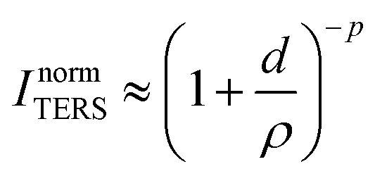 | (1) |
In STM, the gap distance depends on the tunneling parameters, i.e. the tunneling current setpoint, It, and the bias voltage between the tip and sample, Eb. Electron transport between electrodes separated by a thin insulating film in the low bias range is described by Simmons’ equation:21–24
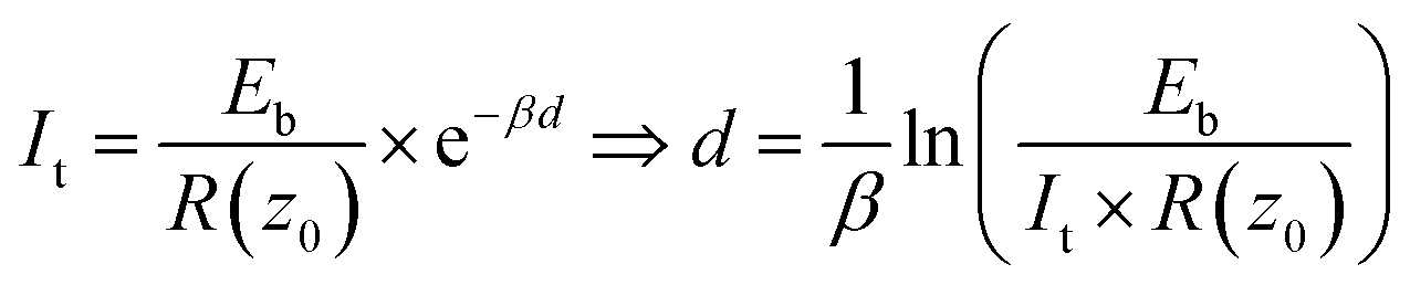 | (2) |
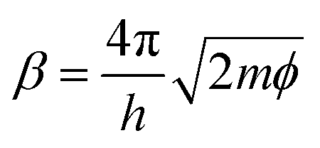 , with work function or barrier height ϕ, electron mass m and Planck’s constant h. According to eqn (2), the tip approaches the sample upon increasing It or decreasing Eb. Combining eqn (1) and (2), we derive an expression relating the TERS intensity to the STM parameters in constant current mode experiments:
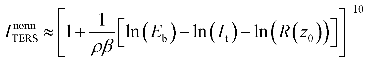 | (3) |
Expression (3) predicts the behaviour of the TER signal intensity as a function of the gap size as determined by the STM parameters. Despite its potential impact on increasing the TERS sensitivity, only a few studies have reported how TER spectra vary with the chosen It and Eb values (ref. 5, 13, 24 and 25) and a systematic study for both It and Eb under identical conditions (same tip, same sample) is still absent. In general, the expected trends were observed in individual studies, i.e. an increasing It results in a rise of the peak and background intensities as expected from the corresponding gap distance decrease,5 and a similar effect has been observed upon decreasing the bias voltage.25 For a monolayer of azobenzene, an unexpected deviation from the STM-parameter dependent distance relation was observed where ITERS decreased with increasing bias voltages faster than would be expected from a mere gap size increase.24 The quantitative discrepancies between model and experiment were suggested to arise from molecular bending induced by the local electric field in the tunneling region created by Eb. Hence, the relationship between Eb and ITERS was suggested to be a convolution of different effects including the gap distance and the related variation of the near-field enhancement magnitude and molecular reordering.
In this paper, we systematically explore the influence of both Eb and It on the TERS response. We compare TERS studies in inert gas (Ar) and in water for a monolayer of thiophenol (PhS) adsorbed on a Au(111) single crystal. We analyse the trends of the intensity changes when varying It and/or Eb. A theoretical model of these effects allows us to predict optimal STM parameters in TERS experiments to exploit maximum signal enhancement and thus experiment sensitivity.
2 Materials and methods
2.1 TERS setup
The home-built TERS setup consists of a commercial STM (Keysight Technologies GmbH, formerly Agilent, 5420) coupled in a side-illumination configuration (55° between the incoming beam and surface normal) with a red He–Ne laser (632.8 nm; REO LSPR-3501, 35 mW maximum output power, linearly polarized). An Olympus 50× long-working-distance objective (WD = 10.6 mm, NA = 0.5) focuses/collects the incident/scattered light. Optical elements (gray filters, mirrors, pinholes) were purchased from Thorlabs. Two filters (a Semrock RazorEdge ultra steep long-pass edge filter LP02-633RE-25 with a cut-off at 79 cm−1 and a Semrock RazorEdge Dichroic LPD02-633RU-25 with a cut-off at 156 cm−1) in the detection path filter out Rayleigh scattering. A Horiba iHR 550 spectrograph with a nitrogen-cooled CCD camera (Symphony II, Horiba) is used as a detector. The optical setup is mounted on an optical table with active vibration isolation. The incoming laser is focused to the tip apex by x, y, and z piezo stages (custom-made by Steinmeyer Mechatronics, formerly Feinmess Dresden, 3 nm precision) that independently move the STM in the x and y directions and the objective in the z direction. Liquid experiments are performed by mounting the sample in a home-built liquid cell. Electrochemically etched Au tips are coated with an insulating layer of Zapon and used for the Ar and liquid experiments. Further details about the optical setup, liquid cell and tip preparation are given elsewhere.132.2 Sample preparation
Ethanol (purity 99.9%), thiophenol and H2O2 (18![[thin space (1/6-em)]](https://www.rsc.org/images/entities/char_2009.gif) 304, 34.5–36.5%) from Sigma-Aldrich, sulfuric acid (purity ≥ 95%) from FisherChem and ultrapure water (Millipore-Q, Milli-Q, resistivity over 18 MΩ) are used in the experiments. To avoid organic contamination during the experiments, we clean all the glassware, teflon tools, liquid cells and substrates by immersing them overnight in piranha solution (H2SO4/H2O2, 3:1) followed by extensive rinsing in boiling Milli-Q water. A Au(111) single crystal of 5N purity (Mateck) is used as the substrate and prepared according to Clavilier’s method.26 The annealed substrate is immersed into 1 mM ethanolic PhS solution for 8 hours and rinsed extensively afterwards to remove adsorbate multilayers. The sample is mounted immediately after preparation. A gentle flow of Ar (5N, Westfalen) is poured over the sample during the experiment (except during spectral acquisition) to prevent contamination.
304, 34.5–36.5%) from Sigma-Aldrich, sulfuric acid (purity ≥ 95%) from FisherChem and ultrapure water (Millipore-Q, Milli-Q, resistivity over 18 MΩ) are used in the experiments. To avoid organic contamination during the experiments, we clean all the glassware, teflon tools, liquid cells and substrates by immersing them overnight in piranha solution (H2SO4/H2O2, 3:1) followed by extensive rinsing in boiling Milli-Q water. A Au(111) single crystal of 5N purity (Mateck) is used as the substrate and prepared according to Clavilier’s method.26 The annealed substrate is immersed into 1 mM ethanolic PhS solution for 8 hours and rinsed extensively afterwards to remove adsorbate multilayers. The sample is mounted immediately after preparation. A gentle flow of Ar (5N, Westfalen) is poured over the sample during the experiment (except during spectral acquisition) to prevent contamination.
2.3 Experimental procedure and analysis
Ar and water experiments were performed on different days and with several different tips following the same procedure and preparation. For each experiment, different series of It (Eb) ramps at constant Eb (It) are taken. Tuning Eb in our STM is achieved by grounding the tip and ramping the sample potential. Due to technical constraints, tuning the bias voltage by changing the potential of the tip while keeping the sample potential constant is only possible in the electrochemical mode. Each experimental series consists of TER spectra taken at different values of It (or Eb) cycled at least once from high to low values and vice versa. It is ramped between 0.1 and 1.8 nA with a constant Eb of 0.02 V, 0.04 V or 0.1 V. Eb is ramped between 0.02 and 0.5 V at a constant It of 1.3, 0.8 or 0.3 nA. For each combination of values, 5 consecutive spectra are taken and the average used for fitting purposes. The STM parameters are ramped under tunneling conditions, and all the spectra in one series are taken at the same location on a flat terrace of the Au(111) substrate as determined by STM topographic imaging prior to the experiment, with the same far-field focussing conditions. The far-field spectra (acquired by retracting the tip 20 nm from the tunneling position) are taken several times during a series by disabling the feedback mechanism of the STM (no motor retraction) to prove the cleanliness and stability of the tip during the hour-long experiments. The same band fitting (masks, background and constraints) is performed on all the spectra from different series and days using Igor PRO (Wavemetrics). Unless stated differently, the results presented in the figures correspond to averages of spectra taken with the same tip under the same conditions (of Eb and It) during scans up and down, and the errors correspond to the standard deviations. The spectra are acquired with integration times of 5 seconds in Ar and of 30 seconds in water with a 600 μW excitation power at the exit of the objective. In the figures, they are presented normalized to the same time and power. Note that signal losses are expected when working in liquid due to beam aberrations and far-field focus distortion.10,133 Results and discussion
The system under study in this work is a monolayer of thiophenol (PhS, inset Fig. 1) adsorbed at a Au(111) single crystal. This sample was chosen because of the strong chemisorption of PhS at Au through the S atom, providing stability to the monolayer and a strong and reproducible TER signal suitable for performing hour-long experiments where many combinations of STM parameters can be explored with the same tip. Additionally, the TERS literature on PhS/Au(111) is extensive which facilitates band assignment and comparisons with previous results.9,13,27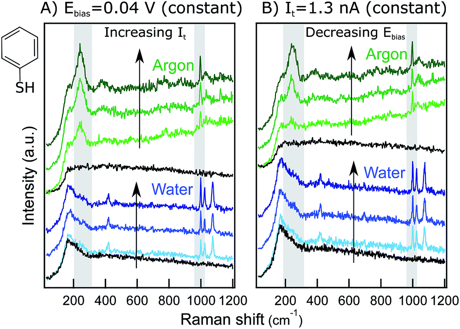 | ||
| Fig. 1 Raw spectra recorded in Ar (green) and in water (blue) for (A) It ramped at a constant Eb of 0.04 V, (B) Eb ramped at a constant It of 1.3 nA. For each series, 20 nm retraction spectra (far-field) are included in black. Gray rectangles indicate marker bands. Spectra are y-offset for clarity. Inset: PhS chemical structure. | ||
Fig. 1 shows examples of raw TER spectra acquired during series with (A) varying It at a constant Eb = 0.04 V and (B) varying Eb at a constant It = 1.3 nA in Ar (green) and in water (blue). The most prominent bands of PhS are visible with a high signal-to-noise ratio (S/N) in all the spectra and are in agreement with previous TERS reports for PhS/Au(111).9,13,27
All the spectra exhibit two prominent bands at ca. 245 cm−1 (δCS + νAuS) and at 997 cm−1 (r–i–d + νCC). In Ar, the spectra also show two weak, broad bands at ca. 390 cm−1 (γCH) and at 1024 cm−1 (νCC + δCH).28 The liquid spectra feature broad far-field bands at low wavenumbers (see the retracted spectra, black), partially masking the 245 cm−1 Au–S band that here is visible only as a shoulder. This far-field peak is present in all the liquid and electrochemical spectra acquired in our lab15 and can be attributed to the aqueous work environment. In the water spectra, the peak at 1024 cm−1 (νCC + δCH) is more prominent than in Ar, and an extra mode at 1074 cm−1 (νCC + δCH) shows up. The weak broad band at 390 cm−1 is not present in the liquid spectra, but an additional sharp peak appears at ca. 420 cm−1 (νCS + νAuS). In the literature, different TER spectral signatures for PhS/Au have been reported whose chemical origin has remained unclear. Additional experiments clarifying the physico-chemical interactions of PhS/Au in Ar and in water are currently under way in our laboratory and will be published elsewhere. Here, we focus the discussion on the relative intensity changes of the Au–S mode at 245 cm−1 and the ring-in-plane deformation mode at 997 cm−1 that are present both in the liquid and in the Ar spectra and are therefore ideal for singling out the influence of STM parameters in different environments. Additionally, given the technical specifications of our instrument, the mode at 245 cm−1 can be used as direct reporter on the effect of the sample potential on the adsorbate–substrate interaction.
Fig. 1A includes three example spectra at increasing It values (from bottom to top), both in Ar and in water. Increasing the tunneling current set-point results in an increase of the marker bands for both the Ar and water experiments. Similarly, ramping the bias voltage to lower values increases the intensity of the marker bands (Fig. 1B). These trends are in qualitative agreement with the expected decrease of the gap distance upon an It increase or Eb decrease. To gain quantitative insight into this relationship, Lorentzian band fittings have been performed for the different series and are discussed in the following sections.
3.1 Influence of the tunneling current set-point, It, on the TER response
Fig. 2 shows the integrated intensities of the 245 cm−1 (A) and 997 cm−1 (B) bands as a function of ln(It) for constant Eb in Ar (0.02 V, green circles; 0.04 V, dark blue squares; 0.1 V, purple triangles) and in water (0.04 V, light blue diamonds). A logarithmic x-axis scale has been chosen because of the gap-distance dependence on It and Eb according to eqn (2). Note that in a linear scale, ITERS as a function of It shows a linear increase upon current increase (see ESI,† Section 1). All the Ar results presented in this figure were acquired on the same day and with the same tip at different locations on a flat Au(111) terrace while the liquid results were taken on a different day with a different tip.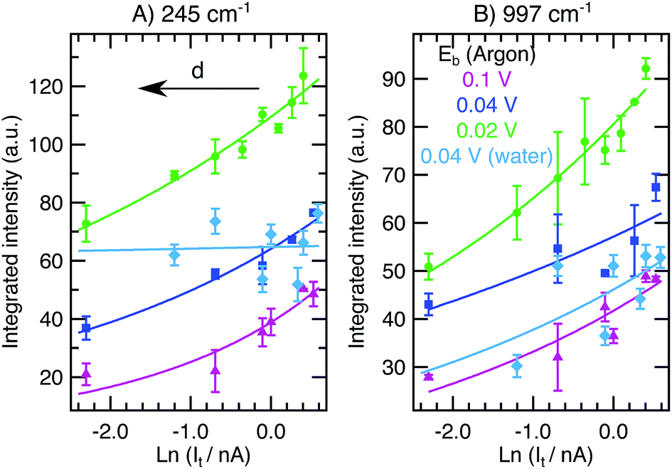 | ||
| Fig. 2 (A) Integrated intensity of the 245 cm−1 mode ((B) 997 cm−1) as a function of ln(It) at constant Eb values of 0.02 V (green circles), 0.04 V (dark blue squares), and 0.1 V (purple triangles) in Ar and 0.04 V in water (light blue diamonds). Averaged results from spectra taken in scans up and down are presented with the standard deviations as the errors. Fittings to eqn (3) are included (solid lines). | ||
We find that ITERS increases upon current increase as expected from a gap distance reduction (eqn (1)–(3)). The value of Eb applied while varying the current has an influence on the absolute TERS intensity. For higher voltages (0.1 V, purple), the overall intensity detected is lower than for lower values (0.02 V, green) in agreement with the larger tip–sample gap expected at high Eb. While there are small differences in the growth rates between the two bands and between different constant values of Eb (see ESI,† Section 1), the average increase in intensity in the scanned set-point range is 87% in Ar and 76% in water. Therefore in a TERS experiment, higher values of tunneling current are preferred if the maximum enhancement is sought both in Ar and liquid experiments. Tuning the current to large values (larger than 1 nA) decreases the gap distance and achieves very high intensities without inducing any obvious chemical change that might further alter the signal intensity or band position (see ESI,† Section 2 for discussion of the Raman shifts) while the tip–sample separation is still large enough to prevent tip crash or contamination.
3.2 Influence of the bias voltage, Eb, on the TER response
Fig. 3 displays the integrated intensities of the 245 cm−1 (A) and 997 cm−1 (B) bands as a function of ln(Eb) for constant values of the tunneling current set-point in Ar (0.3 nA, orange triangles; 0.8 nA, red circles; 1.3 nA, black squares) and water (1.3 nA, light blue diamonds).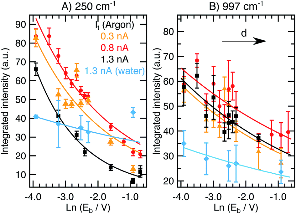 | ||
| Fig. 3 (A) Integrated intensity of the 245 cm−1 mode ((B) 997 cm−1) as a function of Eb at constant It values of 0.3 nA (orange triangles), 0.8 nA (red circles), and 1.3 nA (black squares) in Ar and 1.3 nA in water (light blue diamonds). Averaged results from spectra taken in scans up and down are presented with the standard deviations as the errors. Fittings to eqn (3) are included (solid lines). | ||
Decreasing Eb reduces the tip–sample gap size and therefore results in an increase of ITERS (eqn (1)–(3)) as reported in Fig. 3. From the figure, it is apparent that the choice of It has a negligible effect on the TERS intensity over the investigated Eb range, in contrast to ramping It where ITERS was higher for lower Eb values. The orange, red and black curves in Fig. 3B for the 997 cm−1 peak (taken at 0.3, 0.8 and 1.3 nA, respectively) overlap. For the 245 cm−1 peak, the overall intensity at 1.3 nA is lower than the intensities at 0.3 nA and 0.8 nA. On average (considering both bands and the different values of constant It applied), the intensity increase achieved during the bias ramp is 263% in Ar and 47% in liquid, in contrast with the values of 87% in Ar and 76% in water obtained in the variable current series presented in previous section.
Given these numbers, we conclude that tuning Eb between 0.02 and 0.5 V has a much stronger effect on the gap distance and on the TER signal intensity than ramping It in the range between 0.3 and 1.3 nA. This effect is obvious when plotting the data in Fig. 3 as a function of Eb in a linear scale and comparing it to ITERSvs. It plots (see ESI,† Section 1) where the former exhibits an exponential behavior and the latter a linear trend. When searching for the highest sensitivity in a TERS experiment, higher values of It (higher than 1 nA) and lower values of Eb (under 0.1 V) are preferred, with Eb being the more critical parameter compared to It regarding the TER signal intensity. Interestingly, we find that the described effect on ITERS is smaller in water than it is in Ar for the given parameter space. Further investigations exploring ranges with It > 1.7 nA and Eb < 0.02 V in water could provide more insight into this observation. In general, this first systematic qualitative evaluation allows us to quantitatively correlate the effects of both It and Eb on ITERS.
3.3 Distance dependence model: fitting results
To evaluate if the dependence of the TER signal intensity on the tunneling current set-point and bias voltage follows a simple distance dependence in the case of PhS/Au(111), we fitted the experimental data from Fig. 2 and 3 with eqn (3) (solid lines in the figures) in a free fitting procedure, obtaining ρ, β and R(z0) for each of the series. The averaged fitting results are summarized in Table 1 for the current set-point and bias voltage ramps, for different bands and different values of It and Eb from two different experiments in Ar (with different tips) and one in water. All the fittings were performed with the same initial guesses of the fitting parameters (ρ = 15 nm, β = 0.3 Å−1 and R(z0) = 50 MΩ). The function accurately describes the experimental data in all cases. The obtained values for the tip radius (i.e. dipole radius ρ) from different days, on average 17 ± 3 nm, are in agreement with the average tip sizes produced in our lab as estimated from SEM images.13 ; and tunneling resistance at the landing position R(z0)
| ρ/nm | β/Å−1 | R(z0)/MΩ | |
|---|---|---|---|
| Ar (day 1) | 14 ± 3 | 0.27 ± 0.07 | 34.5 ± 20 |
| Ar (day 2) | 17 ± 6 | 0.36 ± 0.12 | 24.5 ± 10 |
| Ar (average) | 16 ± 2 | 0.32 ± 0.05 | 30 ± 7 |
| Water | 20 ± 2 | 0.33 ± 0.04 | 16 ± 4 |
From fitting, we obtain β values of 0.32 and 0.33 Å−1 in air and in water, respectively. The tunneling decay constant, β, has been measured experimentally for a number of similar molecules in previous works. Frisbie et al.29 found an average β = 0.4 Å−1 for alkanethiols of different lengths, with a tip-to-tip variation in the same range as we find for different days. In ref. 24, β = 0.27 Å−1 was reported for an azobenzene monolayer on Au(111). Electrochemical methods applied to similar aromatic molecules give values of β between 0.35 and 0.57 Å−1.30,31 Our β values lie well within the reported variability. Small discrepancies may be due to differences in the chemical structure, orientation or packing of the monolayer that directly affect the electron transport in the junction.24,32,33 Interestingly, the obtained decay constant values for experiments in Ar and in water are very similar, despite the smaller values of work function that are expected in a liquid.34–36
The values for the junction resistance at the landing position obtained from fitting are 30 and 16 MΩ for air and liquid, respectively. Contact resistance R(−z0)‡ literature values between 0.1 and 50 MΩ have been found for similar molecules, among which a value of ≈0.1 MΩ is found for the PhS/Au(111) system.29,37 Higher values are expected for R(z0) since here the molecular length and gap distance are also considered. Toccafondi et al.24 recently reported R(z0) to be 694 MΩ for azobenzene/Au(111) in a Eb-dependence TERS study. Compared to the literature values, the experimental values of 30 and 16 MΩ that we obtain in Ar and in water, respectively, lie well within the expected range, considering that PhS is shorter than azobenzene. Furthermore, a lower resistance in water is in agreement with the better electric conductivity of MilliQ (resistivity of ca. 18 MΩ) compared to Ar.
In summary, as the fittings quantitatively describe our experimental data points, and the values of the fitting parameters obtained are in agreement with literature values, for both Ar and water and for current set-point and voltage ramps, the TER signal intensity follows the expected distance dependence relationship in eqn (3) for It and Eb ramps, both in Ar and in water. Additional geometric effects such as molecular bending that have been reported for longer molecules24 do not need to be taken into account in the case of PhS/Au(111).
3.4 Raman shift of the Au–S mode
In addition to changes in ITERS, we also observe a shift of the 245 cm−1 band as a function of Eb. In the series of measurements at constant Eb and variable It represented in Fig. 4A, the 245 cm−1 mode appears at a constant position throughout the scanned set-point range. However, the peak maximum is shifted to lower wavenumbers upon Eb increase. This effect is obvious in the series of measurements at constant It and variable bias presented in Fig. 4B. The position of the band at 245 cm−1 experiences a large red-shift upon bias increase independently of the environment or the value of constant set-point applied. The total shift within the potential window scanned is ca. 14 cm−1. Note that no notable Raman shift is detected for the 997 cm−1 band (see ESI,† Section 2).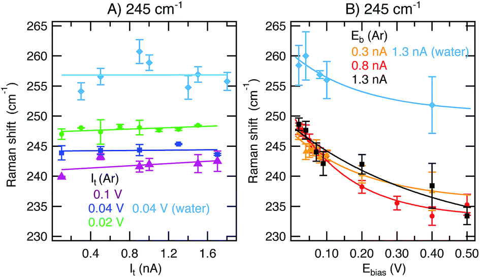 | ||
| Fig. 4 Raman shift of the 245 cm−1 mode as a function of It ((A), at constant Eb values of 0.02 V, green circles; 0.04 V, dark blue squares; 0.1 V in Ar, purple triangles; and 0.04 V in water, light blue diamonds) or Eb ((B), at constant It values of 0.3 nA, orange triangles; 0.8 nA, red circles; 1.3 nA in Ar, black squares; and 1.3 nA in water, light blue diamonds). Averaged results from spectra taken in scans up and down are presented with the standard deviation as the error. Solid lines are included as a guide to the eye. | ||
The fact that only the 245 cm−1 band shifts and only when Eb is ramped can be explained by the changing interaction strength of the S–Au bond when ramping the substrate potential (Eb here due to the technical specifications of our instrument). Upon decreasing Eb, the Au(111) electrode is more positively charged, in this way enabling stronger π(S)–d*(Au) overlap and increased binding strength. A similar effect has been found in an electrochemical TERS study for the N–Au interaction of adenine/Au(111).15 While the paper at hand focuses on the influence of the STM parameters on the TER signature, it would be interesting to quantify the binding strength between PhS and Au as a function of the substrate potential in future experiments and theoretical simulations.
4 Conclusions
We have systematically studied the behaviour of STM-TER spectra as a function of the bias voltage and tunneling current set-point in experiments in Ar and in water. In both cases, for the PhS/Au(111) system, ITERS follows a dependence on the STM parameters expected from a simple gap-distance reduction upon set-point increase or bias decrease. In water, the intensity changes are more moderate than in the Argon experiments. Regarding the absolute intensity increase, tuning the bias voltage in the 0.5 to 0.02 V range results in an exponential band intensity increase while tuning the current set-point in Ar in the range from 0.1 to 1.7 nA shows a linear dependence. In practice, both parameters can be tuned to achieve optimal enhancement factors in STM-TERS experiments with the best results obtained with It > 1 nA and Eb < 0.1 V for the given PhS/Au(111) system under study. If the bias voltage is changed by tuning the potential of the sample with respect to the tip – as is often the case with commercial STMs – the interaction strength of the PhS–Au bond is altered when changing Eb, which manifests itself as a change in the Raman shift of the Au–S stretch vibration while the other band positions in the spectrum remain unchanged. We conclude by pointing out the possibilities that a smart choice of STM parameters presents for ultrasensitive TERS studies of solid/liquid interfaces and/or single molecules.Acknowledgements
KFD is grateful for generous financial support of this work through the Emmy Noether program of the Deutsche Forschungsgemeinschaft (grant no. DO1691/1-1) and through the FP7 Marie Curie Actions ITN-FINON (grant no. 607842). The authors thank Leonie Driessen, Matthias Fenner, Marc-Jan van Zadel and the MPIP electronic workshop for discussions and smart solutions to TERS technical challenges. Open Access funding provided by the Max Planck Society.References
- N. Jiang, D. Kurouski, E. A. Pozzi, N. Chiang, M. C. Hersam and R. P. Van Duyne, Chem. Phys. Lett., 2016, 659, 16–24 CrossRef CAS.
- A. Hartschuh, Angew. Chem., Int. Ed., 2008, 47, 8178–8191 CrossRef CAS PubMed.
- K. F. Domke, D. Zhang and B. Pettinger, J. Am. Chem. Soc., 2006, 128, 14721–14727 CrossRef CAS PubMed.
- W. Zhang, B. S. Yeo, T. Schmid and R. Zenobi, J. Phys. Chem. C, 2007, 111, 1733–1738 CAS.
- R. Zhang, Y. Zhang, Z. C. Dong, S. Jiang, C. Zhang, L. G. Chen, L. Zhang, Y. Liao, J. Aizpurua, Y. Luo, J. L. Yang and J. G. Hou, Nature, 2013, 498, 82–86 CrossRef CAS PubMed.
- N. Chiang, X. Chen, G. Goubert, D. V. Chulhai, X. Chen, E. A. Pozzi, N. Jiang, M. C. Hersam, T. Seideman, L. Jensen and R. P. Van Duyne, Nano Lett., 2016, 16, 7774–7778 CrossRef CAS PubMed.
- A. B. Zrimsek, N. Chiang, M. Mattei, S. Zaleski, M. O. McAnally, C. T. Chapman, A.-I. Henry, G. C. Schatz and R. P. Van Duyne, Chem. Rev., 2017, 117(11), 7583–7613 CrossRef CAS PubMed.
- J.-H. Zhong, X. Jin, L. Meng, X. Wang, H.-S. Su, Z.-L. Yang, C. T. Williams and B. Ren, Nat. Nanotechnol., 2016, 12, 132–136 CrossRef PubMed.
- T. Schmid, B.-S. Yeo, G. Leong, J. Stadler and R. Zenobi, J. Raman Spectrosc., 2009, 40, 1392–1399 CrossRef CAS.
- B. Gjonaj, P. Johnson, M. Bonn and K. F. Domke, Appl. Opt., 2012, 51, 8034–8040 CrossRef PubMed.
- Z.-C. Zeng, S.-C. Huang, D.-Y. Wu, L.-Y. Meng, M.-H. Li, T.-X. Huang, J.-H. Zhong, X. Wang, Z.-L. Yang and B. Ren, J. Am. Chem. Soc., 2015, 137, 11928–11931 CrossRef CAS PubMed.
- D. Kurouski, M. Mattei and R. P. Van Duyne, Nano Lett., 2015, 15, 7956–7962 CrossRef CAS PubMed.
- N. Martín Sabanés, L. Driessen and K. F. Domke, Anal. Chem., 2016, 88, 7108–7114 CrossRef PubMed.
- M. Mattei, G. Kang, G. Goubert, D. V. Chulhai, G. C. Schatz, L. Jensen and R. P. Van Duyne, Nano Lett., 2016, 17, 590–596 CrossRef PubMed.
- N. Martín Sabanés, T. Ohto, D. Andrienko, Y. Nagata and K. F. Domke, Angew. Chem. Int. Ed., 2017, 56, 9796–9801 CrossRef PubMed.
- B. Pettinger, K. F. Domke, D. Zhang, G. Picardi and R. Schuster, Surf. Sci., 2009, 603, 1335–1341 CrossRef CAS.
- I. Notingher and A. Elfick, J. Phys. Chem. B, 2005, 109, 15699–15706 CrossRef CAS PubMed.
- B. Pettinger, K. F. Domke, D. Zhang, R. Schuster and G. Ertl, Phys. Rev. B: Condens. Matter Mater. Phys., 2007, 76, 113409 CrossRef.
- L. G. Cançado, A. Jorio, A. Ismach, E. Joselevich, A. Hartschuh and L. Novotny, Phys. Rev. Lett., 2009, 103, 1861011–1861014 CrossRef PubMed.
- R. V. Maximiano, R. Beams, L. Novotny, A. Jorio and L. G. Cançado, Phys. Rev. B: Condens. Matter Mater. Phys., 2012, 85, 1–8 CrossRef.
- J. G. Simmons, J. Appl. Phys., 1963, 34, 1793–1803 CrossRef.
- E. Meyer, H. J. Hug and R. Bennewitz, Scanning Probe Microscopy: the lab on a tip, Springer-Verlag, Berlin Heildelberg GmbH, 1st edn, 2004 Search PubMed.
- R. L. McCreery, Chem. Mater., 2004, 16, 4477–4496 CrossRef CAS.
- C. Toccafondi, G. Picardi and R. Ossikovski, J. Phys. Chem. C, 2016, 120, 18209–18219 CAS.
- Y. Fujita, N. N. Horimoto, S. Kajimoto and H. Fukumura, Chem. Phys. Lett., 2013, 582, 110–114 CrossRef CAS.
- J. Clavilier, R. Faure, G. Guinet and R. Durand, J. Electroanal. Chem. Interfacial Electrochem., 1979, 107, 205–209 CrossRef.
- C. Blum, L. Opilik, J. M. Atkin, K. Braun, S. B. Kämmer, V. Kravtsov, N. Kumar, S. Lemeshko, J. F. Li, K. Luszcz, T. Maleki, A. J. Meixner, S. Minne, M. B. Raschke, B. Ren, J. Rogalski, D. Roy, B. Stephanidis, X. Wang, D. Zhang, J. H. Zhong and R. Zenobi, J. Raman Spectrosc., 2014, 45, 22–31 CrossRef CAS.
- C. G. T. Feugmo and V. Liégeois, ChemPhysChem, 2013, 14, 1633–1645 CrossRef PubMed.
- D. J. Wold, R. Haag, M. A. Rampi and C. D. Frisbie, J. Phys. Chem. B, 2002, 106, 2813–2816 CrossRef CAS.
- S. B. Sachs, S. P. Dudek, R. P. Hsung, L. R. Sita, J. F. Smalley, M. D. Newton, S. W. Feldberg and C. E. D. Chidsey, J. Am. Chem. Soc., 1997, 119, 10563–10564 CrossRef CAS.
- S. Creager, C. J. Yu, C. Bamdad, S. O. Connor, T. Maclean, Y. Chong, G. T. Olsen, J. Luo, M. Gozin, J. F. Kayyem and E. Lam, J. Am. Chem. Soc., 1999, 121, 1059–1064 CrossRef CAS.
- H. Yamamoto and D. H. Waldeck, J. Phys. Chem. B, 2002, 106, 7469–7473 CrossRef CAS.
- L. Venkataraman, J. E. Klare, C. Nuckolls, M. S. Hybertsen and M. L. Steigerwald, Nature, 2006, 442, 904–907 CrossRef CAS PubMed.
- J. Pan, T. W. Jing and S. M. Lindsay, J. Phys. Chem., 1994, 98, 4205–4208 CrossRef CAS.
- J. Halbritter, G. Repphun, S. Vinzelberg, G. Staikov and W. J. Lorenz, Electrochim. Acta, 1995, 40, 1385–1394 CrossRef CAS.
- M. Hugelmann and W. Schindler, Surf. Sci., 2003, 541, L643–L648 CrossRef CAS.
- H. H. B. Akkerman, B. de Boer and B. D. Boer, J. Phys.: Condens. Matter, 2008, 20, 13001 CrossRef.
Footnotes |
| † Electronic supplementary information (ESI) available. See DOI: 10.1039/c7fd00164a |
| ‡ While R(−z0) accounts for the resistance of the junction in contact between the tip and sample, the parameter in eqn (3), R(z0), is the junction resistance at the landing position. |
| This journal is © The Royal Society of Chemistry 2017 |