
 Open Access Article
 This Open Access Article is licensed under a
 Creative Commons Attribution 3.0 Unported Licence
Understanding the morphology of solution processed fullerene-free small molecule bulk heterojunction blends†
Andrew
Namepetra
ab,
Elizabeth
Kitching
b,
Ala'a F.
Eftaiha
*c,
Ian G.
Hill
a and
Gregory C.
Welch
*d
aDepartment of Physics, Dalhousie University, 1459 Oxford Street, Halifax, Nova Scotia, Canada B3H 4R2. E-mail: ian.hill@dal.ca
bDepartment of Chemistry, Dalhousie University, Nova Scotia, Canada B3H 4R2
cDepartment of Chemistry, The Hashemite University, P.O. Box 150459, Zarqa 13115, Jordan. E-mail: alaa.eftaiha@hu.edu.jo
dDepartment of Chemistry, University of Calgary, Calgary, Alberta, Canada. E-mail: gregory.welch@ucalgary.ca
First published on 31st March 2016
Abstract
Bulk-heterojunction (BHJ) molecular blends prepared from small molecules based on diketopyrrolopyrrole (DPP) and perylene-diimide (PDI) chromophores have been studied using optical absorption, cyclic voltammetry, photoluminescence quenching, X-ray diffraction, atomic force microscopy, and current–voltage measurements. The results provided useful insights into the use of DPP and PDI based molecules as donor–acceptor composites for organic photovoltaic (OPV) applications. Beside optoelectronic compatibility, the choice of active layer processing conditions is of key importance to improve the performance of BHJ solar cells. In this context, post-production treatments, viz. thermal and solvent vapour annealing, and the use of 1,8-diiodooctane as a solvent additive were employed to optimize the morphology of blend films. X-ray diffraction and atomic force microscopy indicated that the aforementioned processing strategies led to non-optimal composite morphologies with significantly large crystallites in comparison to exciton diffusion lengths. Although the open circuit voltage of the OPV devices was satisfactory (0.78 V), it was anticipated that the bulky domains hamper charge dissociation and transport, which resulted in low photovoltaic performance.
Introduction
Solution processable organic photovoltaic (OPV) cells provide an outstanding and inexpensive platform to harvest solar energy using flexible substrates compatible with printing and coating techniques suited for high-volume production. Being lightweight, coloured and semi-transparent, OPV cells are of commercial interest for a wide range of applications such as power-generating windows and decorative lighting systems with reduced transportation and installation cost.1–6The conversion of solar energy into electricity in bulk-heterojunction (BHJ) OPV cells depends on the energetic offset between a two-component system comprised of a donor material with large ionization potential and an acceptor material of high electron affinity to overcome the strong columbic interactions between photogenerated electron–hole bound pairs (excitons) at the donor–acceptor interface.6,7 Current state-of-the-art OPV cells adopt polymer donors and fullerene derivative acceptors.8–10 There are several limitations that hold back further development of polymer–fullerene OPV (see the reviews by our group7,11,12 and others13–15 for more details about the inherent drawbacks of polymeric materials and fullerenes). In this respect, small organic molecules offer several advantages such as easy synthesis, well-defined molecular structures and readily tuneable optical and electronic properties, which make them promising alternatives for polymers and fullerenes in BHJ solar cells.16,17 To date, the maximum power conversion efficiency (PCE) reported for photovoltaic cells based upon molecular donor and non-fullerene small acceptor molecules is 5.44%,18 which is significantly lower than the record for OPV cells based upon molecular donor–fullerene acceptors (between 8 and 10%),19–21 and polymer donor–molecular acceptors (approaching 7%),22,23 which means that significant advances still need to be made in this research area. To boost the efficiency of molecular solar cells, efforts are directed towards developing molecular entities of improved optical and charge transporting properties, engineering the morphology of donor–acceptor blends to attain efficient charge separation and collection, as well as upgrading device architectures.
Among various small molecules developed for organic solar cells, diketopyrrolopyrrole containing materials (DPP, the chemical structure is shown in Scheme 1A) have attracted great attention due to their strong visible-light absorption24 and excellent charge transport properties,25 which make DPP based materials potential candidates for a broad range of optical and electronic applications.26,27 Nguyen and co-workers28–35 have reported on the design, synthesis, self-assembly and photovoltaic performance of DPP core molecules as donor materials in fullerene BHJ solar cells (Scheme 1B). It has been reported that DPP core molecules end-capped with π-stacking moieties exhibited PCE between 4 and 5.3% when blended with different fullerene derivatives such as phenyl-C71-butyric acid methyl ester36 and methano indene fullerene in BHJ OPV cells.37 The strong electron-withdrawing nature of DPP makes it possible to be exploited as an n-type organic semiconductor.7,26 Jung and Jo reported a non-fullerene molecular acceptor composed of DPP and benzothiadiazole with a PCE of 5.0% when combined with thieno[3,4-b]thiophene/benzodithiophene (PTB7) as an electron donor.38
 | ||
| Scheme 1 Chemical structures of: (A) diketopyrrolopyrrole (DPP) chromophore. (B) Aryl-DPP based derivatives (Ar = phenyl (Ph), thienyl (Th) & furyl (Fu), and R = alkyl side chains). (C) DPP based small donor molecule of the acceptor–donor–acceptor–donor–acceptor (A1–D–A2–D–A1) framework. (D) Perylene diimide and its 2-ethylpropyl derivative. | ||
Recently, our group has reported on the design of a small molecule within the terminal acceptor–donor bridge–acceptor core–donor bridge–terminal acceptor (A1–D–A2–D–A1) framework.39–41 Dithiophenediketopyrrolopyrrole (DPPTh2) incorporating electron-deficient phthalimide and naphthalimide end-capping units that bear different alkyl side chains synthesized using microwave-assisted direct heteroarylation (DHA) methods was of particular interest.41 The results indicated that those compounds have narrow band-gaps and deep frontier energy levels, which make them potential candidates as electron transporting materials. Our design strategy of new OPV materials has been directed toward the use of sustainable moieties with proven photovoltaic potential. In this respect, furan derivatives have often been considered more sustainable alternatives than thiophene counterparts because they can be synthesized from a variety of natural products.42 We have reported that substituting thiophene by furan can alter the electronic performance of molecular semiconductors significantly.43 As a step toward achieving sustainability, we have replaced furan with thiophene to synthesize a bis-furandiketopyrrolopyrrole (DPPFu2) based semiconductor using a silica supported palladium catalyst system as described lately by our group.44 As depicted in Scheme 1C, our design utilizes phthalimide (Pht) and DPP as terminal end and central core acceptor units, respectively, and furan as a π-conjugated bridge.
As a strong electron-deficient molecule, perylene-diimide (PDI, Scheme 1D) has been used to synthesize solution processable n-type small molecules with tailored electronic and optical properties.45,46 The strong π–π interactions lead to over crystallization of PDI based molecules, which diminish exciton dissociation at the donor–acceptor interface of BHJ blends and thus limit achieving high PCE values comparable to fullerene derivatives. To overcome the formation of large crystallites, the design strategies of PDI based molecules have been directed to reduce π–π stacking, without influencing the charge transport properties either by preparing PDI dimers with a highly twisted dimeric backbone47–50 or through functionalization of the PDI monomer by alkyl substituents,51 particularly, the 2-ethylpropyl (EP) side chain.52–54 Yan and co-workers reported a three dimensional electron acceptor based on the tetraphenylethylene core flanked with four PDI units with a PCE of 5.53% when combined with a donor polymer.55 In this regard, monomeric PDI is more attractive than its dimeric counterparts due to the more simple synthesize procedures.
As shown above, literature reports highlight the potential utility of DPP and PDI based compounds to act as donor and acceptor materials when blended with polymers and fullerene derivatives through exploiting different design strategies. However, there are a limited number of reports that demonstrate the impact of processing conditions56–59 on their blends to fabricate high performance “fullerene-free all molecule” OPV cells. In this context, Yao's research group60,61 indicated that the efficiency of solution processed solar cells comprised of the DPP donor and the PDI acceptor improved drastically when 1,8-diiodooctane (DIO) was used as a solvent additive. In this study, we have investigated different thin film processing strategies, viz. thermal annealing, the usage of solvent additives and solvent vapour annealing (SVA) to understand the precise nature of thin films made of DPP(Fu-Pht)2 and EP-PDI to uncover factors that govern self-assembly processes of film components when transitioning from solution into the solid state. Spin casting has been used to prepare donor–acceptor blend films. UV-vis absorption–emission spectroscopy and cyclic voltammetry (CV) have been carried out to determine the optical properties of the film components and to examine how excitons dissociate at the donor–acceptor interface. Surface-sensitive diffraction and microscopy techniques, namely X-ray diffraction (XRD) and atomic force microscopy (AFM), have been used to examine the molecular-level organization of donor–acceptor domains throughout the study. While neither of the techniques provides all of the information necessary to characterize the blend films thoroughly, both of them can give complementary information to guide future optimization efforts.
Results and discussion
A. Optical and electrochemical properties
The absorption properties of DPP(Fu-Pth)2 and EP-PDI were determined using UV-visible spectroscopy. The absorption spectra of the two compounds in chloroform (CHCl3) solution and thin films are shown in Fig. 1. Starting with DPP(Fu-Pth)2, the absorption profile in solution displays three distinct absorption bands at ca. 390, 575 and 620 nm (Fig. 1A), which is consistent with those reported elsewhere in the literature for other DPP based small molecules.28,41 The first vibronic band is attributed to the localized π–π transitions, and the other low energy bands are ascribed to the charge transfer within the core unit.29 The absorption profile of the thin film is slightly red-shifted compared to the solution spectrum. The shift might be attributed to a more planar structure in the solid state that enhances electron delocalization. In comparison with a similar DPP based compound featuring thiophene bridges,41 replacement of thiophene with furan (dipole moments are 0.53 and 0.67 Debye, respectively)62 shifts the vibronic bands into lower wavelengths. EP-PDI has three absorption peaks at ca. 460, 490 and 525 nm (Fig. 1B). Upon transitioning from solution to thin-films, a broadening and red shift in the absorption spectrum are observed. This shift is common for conjugated molecules and can be explained by the aggregation of adjacent molecules in the solid state as they aligned in a head-to-tail configuration, known as J-aggregation.63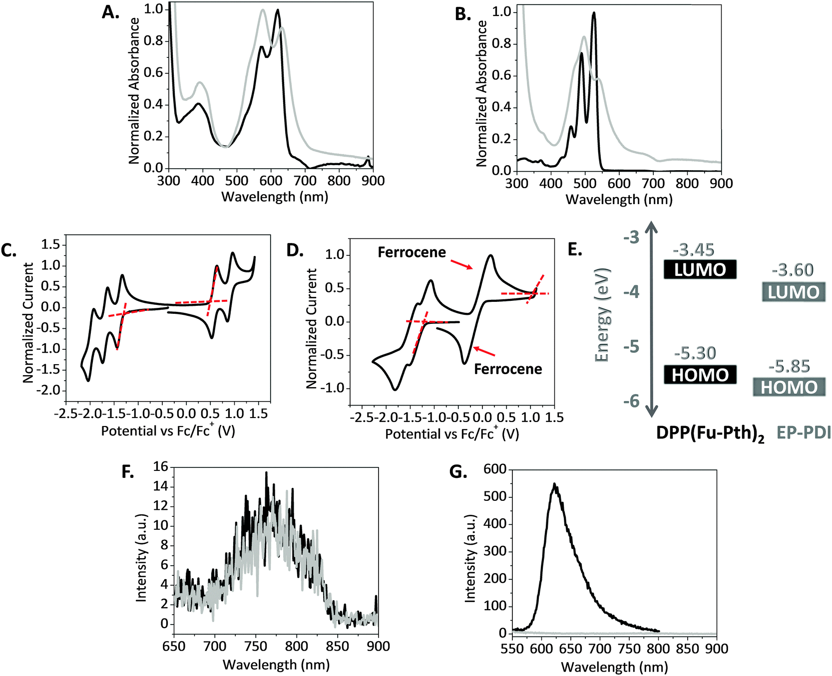 | ||
| Fig. 1 Normalized UV-vis absorbance spectra in CHCl3 solution (black) and thin films (light gray) spun from CHCl3 solution of: (A) DPP(Fu-Pth)2. (B) EP-PDI. Cyclic voltammograms obtained in CH2Cl2 solution under nitrogen using a sweep rate of 100 mV s−1 for: (C) DPP(Fu-Pth)2. (D) EP-PDI. (E) Band structure diagram illustrating the orbital energies of DPP(Fu-Pth)2 and EP-PDI obtained from CV. E(HOMO) = −(Eox + 4.80) [eV] and E(LUMO) = −(Ered + 4.80) [eV], where Eox and Ered are the oxidation and reduction onsets shown in C and D. PL emission spectra of neat (black) and blend films (gray) spun from CHCl3 solutions of: (F) DPP(Fu-Pth)2 and its blend excited at 576 nm (λmax of DPP(Fu-Pth)2). (G) EP-PDI and its blend excited at 497 nm (λmax of EP-PDI). | ||
The electrochemical properties of the two compounds were measured using cyclic voltammetry in dichloromethane (CH2Cl2) solutions. While DPP(Fu-Pth)2 oxidizes reversibly at 0.5 V, EP-PDI exhibits an irreversible oxidization at 1.05 V, owing to the molecule's electron deficient character. Both compounds experience reversible reduction at 1.35 V for the former and 1.2 V for the latter (Fig. 1C and D). The EP-PDI values are in a good agreement with the previous reports.14,64 From these values, a band structure diagram that illustrates the highest occupied molecular orbital (HOMO) and lowest unoccupied molecular orbital (LUMO) of the two compounds are shown in Fig. 1E. The HOMO and LUMO offsets are appropriate for both Channel I and Channel II processes if the two compounds are combined for OPV applications.65
The ability of the blend components to quench the fluorescence emission of photoexcited species was examined using photoluminescence (PL) spectroscopy and is shown in Fig. 1. The emission spectra were measured after exciting neat and blend films at the absorption maxima obtained from the absorption spectra of DPP(Fu-Pth)2 and EP-PDI films. On the one hand, the fluorescence spectrum of the blend film excited at 576 nm is equivalent to that recorded for the DPP(Fu-Pth)2 film (Fig. 1F). On the other hand, the fluorescence spectrum of the EP-DPI film excited at 497 nm is reduced to null by the blend film (Fig. 1G). The weak PL signal of DPP(Fu-Pth)2, which could be anticipated to background emission or large domain sizes, does not provide any conclusive evidence about electron transfer that is expected to take place from the photoexcited donor LUMO to the acceptor LUMO. The fluorescence quenching of EP-PDI might be designated to energy transfer from EP-PDI to DPP(Fu-Pth)2 rather than photoexcited electron transfer since EP-PDI emits light where DPP(Fu-Pth)2 absorbs.
B. As-cast blend films
The UV-vis spectra of as-cast blend films, viz. 3![[thin space (1/6-em)]](https://www.rsc.org/images/entities/char_2009.gif) :1, 1:1 and 1:3 DPP(Fu-Pth)2:EP-PDI, indicated a relatively broad absorption in the visible region between 400 and 635 nm (Fig. 2A). It is anticipated that the complementary absorption profiles of the two materials should maximize the light harvesting ability of their composites if both are combined for OPV applications. The crystallinity and molecular-level organization of as-cast blend films were measured using XRD and AFM. The diffraction patterns show no detectable peaks within the measured range. AFM images reveal large domains regardless of the blend ratio. The image of the 3:1 blend shows finger-like striations accompanied by large islands up to a micron in breadth. The image of the films comprised of 1:3 blend indicates that columnar features are scattered across the surface of the film. The morphology of the 1:1 blend is in between the aforementioned two. Herein, the tendency of the molecular species to self-aggregate results in large domain sizes compared to the exciton diffusion length (<100 nm),66–69 which is a limiting factor in attaining high PCE values if both compounds are utilized for OPV applications. Literature reports indicated that obtaining well-ordered interpenetrating networks of donors and acceptors through employing active layer processing strategies would play a significant role in achieving high performance solar cells.12,70,71
:1, 1:1 and 1:3 DPP(Fu-Pth)2:EP-PDI, indicated a relatively broad absorption in the visible region between 400 and 635 nm (Fig. 2A). It is anticipated that the complementary absorption profiles of the two materials should maximize the light harvesting ability of their composites if both are combined for OPV applications. The crystallinity and molecular-level organization of as-cast blend films were measured using XRD and AFM. The diffraction patterns show no detectable peaks within the measured range. AFM images reveal large domains regardless of the blend ratio. The image of the 3:1 blend shows finger-like striations accompanied by large islands up to a micron in breadth. The image of the films comprised of 1:3 blend indicates that columnar features are scattered across the surface of the film. The morphology of the 1:1 blend is in between the aforementioned two. Herein, the tendency of the molecular species to self-aggregate results in large domain sizes compared to the exciton diffusion length (<100 nm),66–69 which is a limiting factor in attaining high PCE values if both compounds are utilized for OPV applications. Literature reports indicated that obtaining well-ordered interpenetrating networks of donors and acceptors through employing active layer processing strategies would play a significant role in achieving high performance solar cells.12,70,71
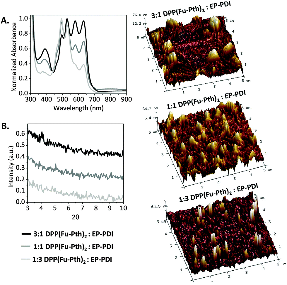 | ||
| Fig. 2 (A) Normalized UV-vis absorbance spectra of as-cast blend films spun from CHCl3 solutions. (B) X-ray diffraction patterns of as-cast blend films spun from CHCl3 solutions. 3D-AFM height mode images (5 μm × 5 μm) of the as-cast blend films of are shown at the right side. The root mean square (RMS) roughness values of the 3:1, 1:1 and 1:3 blends are 17.1, 15.3 and 37.1 nm, respectively. | ||
C. Thermal annealing
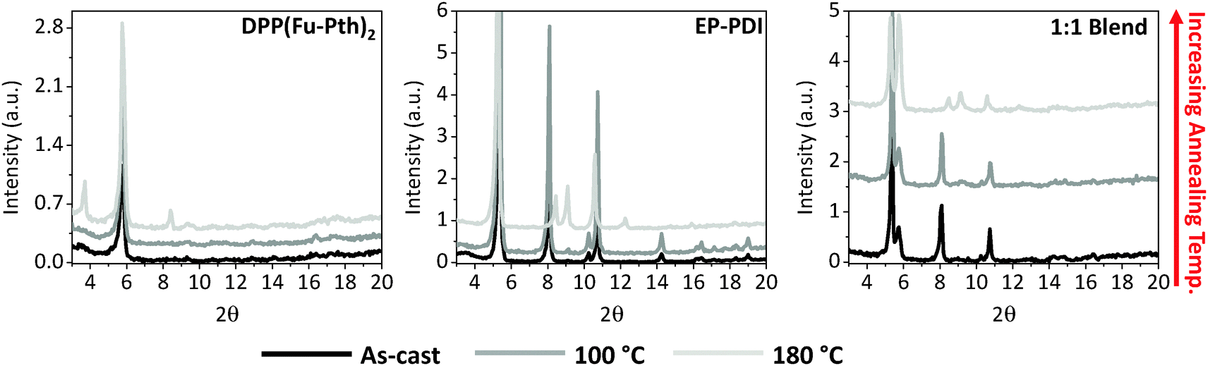
Post-deposition thermal annealing is one of the proposed strategies to engineer the morphology of donor–acceptor composites.72 The optical absorption and XRD patterns of the neat and blend films in response to different annealing temperatures have been investigated and shown in Fig. 3. The absorption profile of the as-cast DPP(Fu-Pth)2 neat film is characterized by three major absorption bands at 395, 576 and 632 nm. After annealing at 100 and 120 °C, there is a broadening and hypsochromic shift in the middle absorption band. Annealing between 140 and 180 °C results in a red shift in the low-energy band (from 632 to 662 nm) and the appearance of a new peak in the intermediate band. A new high-energy peak is also observed at 350 nm. The absorption spectrum of the as-cast EP-PDI neat film reveals three major bands at ca. 497, 540 and 570 nm, corresponding to the 0–0, 0–1 and 0–2 transitions, respectively.54 Unlike DPP(Fu-Pth)2, the profiles of the thermally annealed EP-PDI films are quite similar to that obtained for the as-cast one. The spectrum of the as-cast blend film shows six bands, each corresponding to those observed for each individual component. After annealing, the observed changes in the absorption spectra are analogous to those observed in the neat film except two features. Interestingly, the relative intensity of the peak at 497 nm (corresponds to EP-PDI) is significantly reduced and the 0–1 peak identified at 540 nm is red-shifted to 555 nm. This suggests that the DPP based molecule influences the order of EP-PDI in the solid state upon heating, which affects the electronic nature of the material in the blend film.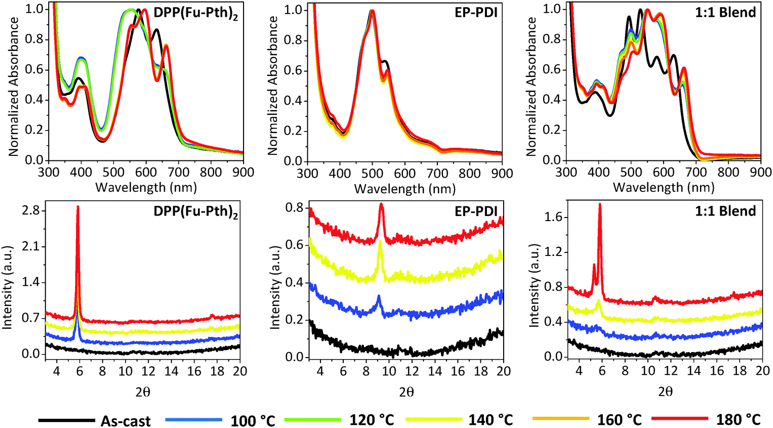 | ||
| Fig. 3 UV-vis absorption spectra (upper raw) and XRD patterns (lower raw) of neat and 1:1 DPP(Fu-Pth)2:EP-PDI blend films. | ||
To gain knowledge about the influence of thermal annealing on crystallinity, XRD patterns of the neat and blend films before and after annealing have been investigated (Fig. 3). The patterns of the as-cast films (both neat and blend) show no detectable peaks within the measured range, which can be explained either by the presence of extremely small crystalline domains that could not be detected using simple powder XRD techniques or an amorphous structure of the films. After annealing the neat films at 100 °C, new peaks are emerged at 5.8 and 9.1° for DPP(Fu-Pth)2 and EP-PDI films, respectively. Successive annealing at higher temperatures increases the intensity of the abovementioned peaks, which reflect the tendency of the crystalline domain to grow up. A plausible mechanism for domain growth as a function of temperature is Ostwald ripening, in which small domains merge to form larger domains (vide infra).
The diffraction patterns of the thermally annealed blend show the peak observed for the annealed DPP(Fu-Pth)2 film (2θ = 5.8°), but not for EP-PDI. At 140 °C, a second peak arose at around 10.8°. A further increase in annealing temperature up to 180 °C results in the emergence of a third peak at 5.3°, which is not observed for neither DPP(Fu-Pth)2 nor EP-PDI neat films. It is also important to note that the peak at 9.1° in the EP-PDI neat film is not observed in the diffraction pattern of the blend film. This may suggest that the PDI based molecule adopts a different crystalline phase in the blend film.
In order to improve the signal-to-noise of our XRD measurements, which might unveil new diffraction peaks for the neat films, the XRD patterns of drop-cast neat and blend films have been investigated and presented in Fig. 4. The DPP(Fu-Pth)2 film shows a peak at 5.8° even before thermal annealing. Exposure of the film to higher temperatures results in two peaks at 3.8 and 8.2° that are not observed for the spin-cast counterpart. On the other hand, similar to the spin-cast EP-PDI film, the peak at 9.1° does not emerge until the drop-cast film is exposed to heat. In addition, several new peaks are identified that are not observed before in the corresponding neat, spin-cast film. Two of them, namely 5.3 and 10.8°, are recognized when the spin-cast blend is thermally annealed. Moreover, the drop-cast blend film exhibits four diffraction peaks at 5.3, 5.8, 8.1, and 10.8°. Upon increasing the annealing temperature, the intensity of the 5.8° peak is increased at the expense of 5.3°. This suggests that DPP(Fu-Pth)2 crystallites have a more preferential orientation over EP-PDI domains upon annealing.
 | ||
| Fig. 4 XRD patterns of drop-cast neat and blend films. | ||
AFM topographic images of spin-cast (neat and blend) films were explored to correlate the observed changes in crystallinity with the surface morphology. As shown in Fig. 5, the as-cast DPP(Fu-Pth)2 film consists of flat, flake-like domains. After annealing, finger-like striations appear to be dominant. These features are assumed to be crystalline when considering the XRD patterns (as presented in Fig. 3). A further increase in the annealing temperature (up to 180 °C) results in large cubic crystals. Moreover, surface roughness increases with increasing annealing temperature (RMS roughness values are 1.74, 6.27, 7.88 and 13.0 nm for the as-cast film and those annealed at 100, 140 and 180 °C, respectively). The image of the as-cast EP-PDI film shows large micro-sized flakes. After annealing at 100 °C, small columnar features start to cover the surface of the flakes (presumably corresponding to the 9.1° diffraction peak). Annealing at higher temperatures results in considerable growth. The image of the as-cast blend film consists of “islands” emerging from a relatively flat background marked with striations. This results in lowering the RMS roughness values from 50.5 nm for the as-cast film to 27.0 from the film annealed at 140 °C. Exposing the film to elevated temperatures triggers the formation of needle shape structures that are merged as the temperature is increased (RMS roughness is 135 nm). The observed size-temperature dependence of domain growth suggests that Ostwald ripening is the mechanism that controls domain growth as a function of temperature (vide supra). The images of the blend films indicate that thermal annealing results in the formation of needle-shaped crystallites that become larger and rougher as a function of temperature (RMS roughness values are 8.72, 12.3 and 25.2 nm for those annealed at 100, 140 and 180 °C, respectively).
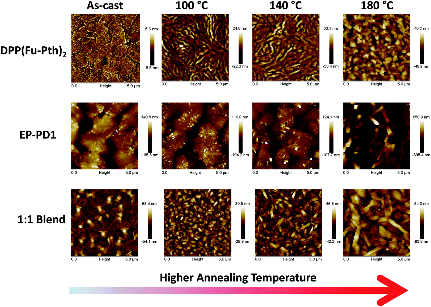 | ||
| Fig. 5 AFM height mode images (5 μm × 5 μm) of neat and blend films spun from CHCl3 solutions before and after sequential thermal annealing. | ||
D. Solvent vapour annealing (SVA)
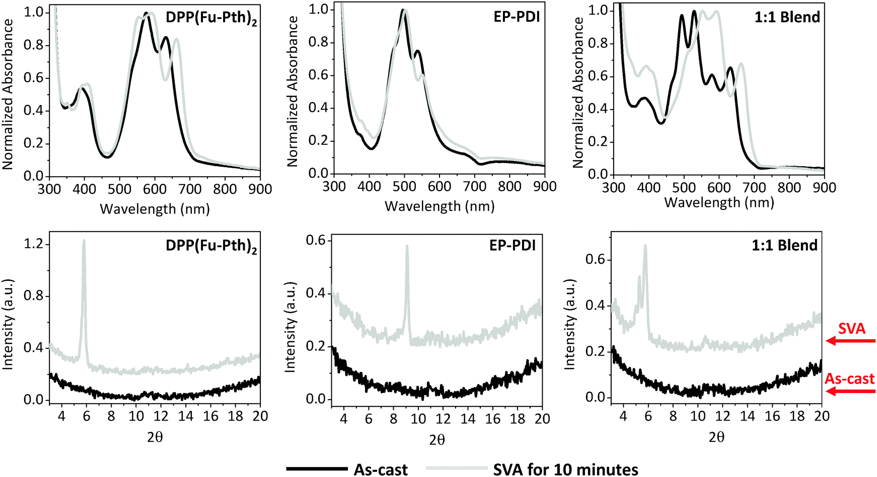
SVA can be used as an alternative postproduction processing protocol to induce changes in the nanoscale morphology through exposing thin films to solvent vapours for a certain period.72–74 It is interesting to understand how different post-treatment strategies, viz. thermal and solvent vapour annealing, alter the self-organization of neat and blend films. The UV-vis absorption profiles and XRD patterns of neat and blend films annealed by CHCl3 vapour are presented in Fig. 6. After 10 minutes in the annealing chamber, the absorption profile of the DPP(Fu-Pth)2 film undergoes a red-shift and the most intense peak is broadened. While annealing the EP-PDI film causes a reduction in intensity of the low-energy band (at 540 nm), the profile of the 1:1 blend film shows two notable changes. Firstly, an increase in the intensity of the DPP(Fu-Pth)2 peak at ca. 396 nm and secondly, a reduction in the intensity of the EP-PDI peak at 470 nm (0–1 transition) are observed. A weakening of the latter peak is generally associated with enhanced ordering of PDI molecules in the solid-state.54 It should be noted that all the observed changes in the absorption spectra of the neat and blend films after SVA are very similar to those obtained after thermal annealing (Fig. 3).
 | ||
| Fig. 6 UV-vis absorption spectra (upper raw) and XRD patterns (lower raw) of neat and 1:1 DPP(Fu-Pth)2:EP-PDI blend films. | ||
It is clear that SVA induces crystal growth as evidenced by the new diffraction peaks. The patterns of neat films show two characteristic peaks after vapour annealing at 5.7° and 9.1° for DPP(Fu-Pth)2 and EP-PDI, respectively (Fig. 6). Interestingly, the 9.1° peak is absent in the blend film after annealing. Nevertheless, the peak at 5.3°, which has been shown to be characteristic of EP-PDI neat films, is shown in Fig. 4. Consistent with thermally annealed films, the XRD results imply that the EP-PDI crystals grow in a different preferential orientation compared to the neat film. Given the presence of the peak at 5.7° in both DPP(Fu-Pth)2 neat and blend films, the crystal growth of DPP(Fu-Pth)2 is induced by SVA and is not influenced by the presence of EP-PDI.
AFM images of the vapour-annealed films indicated that DPP(Fu-Pth)2 becomes more textured after SVA, which might indicate the growth of crystalline domains (Fig. 7). The morphology of the EP-PDI film also changes, where needle-shaped crystallites are noticed. The 1:1 blend is composed of randomly oriented needle-shaped crystallites, microns in length. Such a morphology is clearly inappropriate for use in OPV cells due to the large domain sizes.75
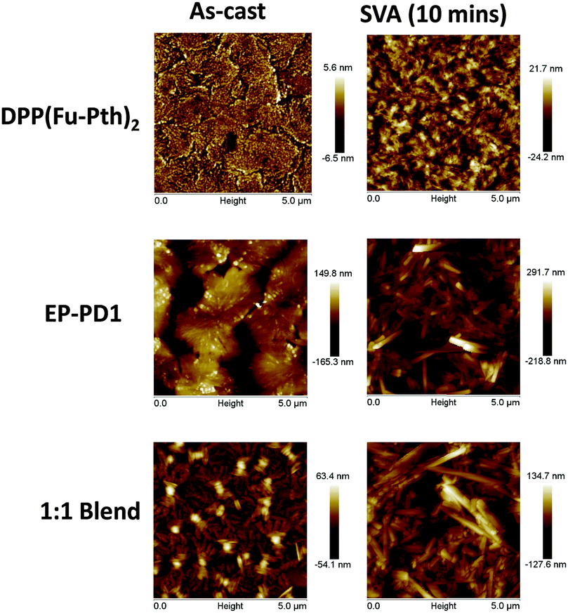 | ||
| Fig. 7 AFM height mode images (5 μm × 5 μm) of neat and blend films spun from CHCl3 solutions before and after SVA annealing for 10 minutes. | ||
E. The use of solvent additives
The impact of solvent additives on the morphological characteristics of donor–acceptor composites has been examined to improve materials and processing designs.58,71,76–78 In this study, the influence of 1,8-diiodooctane (DIO) on the neat and blend films was investigated using UV-vis spectroscopy, XRD and AFM (Fig. 8 and 9, respectively). Compared with the as-cast DPP(Fu-Pth)2 film, the addition of 0.4% DIO results in a blue shift in the high-intensity band (from 576 to 522 nm) and a drastic reduction in the intensity of the peak at 633 nm, this is indicative of H-aggregation of the DPP chromophore. Curiously, the profile of the film cast from a solution with 0.8% DIO shows a red shift in the low-energy band from 633 nm to 664 nm, typical of J-aggregation, thus DIO is an effective additive to tune the aggregation behaviour of this DPP molecule.79 The EP-PDI film containing 0.4% (v/v) DIO shows an increase in the intensity of the high-energy absorption peak at 377 nm while causing a red shift in the 0–0 transition from 536 nm to 553 nm and the emergence of a new peak is observed at 595 nm. No significant differences in the absorption profile are observed in the film cast from solution with a doubled amount of DIO. Blend films cast from solutions with 0.4% DIO display no change in the position of the bands, but an increase in intensity of the low-energy bands of DPP(Fu-Pth)2. Casting films from solutions of 0.8% DIO concentration changes the positions of the absorption bands of the two components. While the XRD patterns of the neat films loaded with 0.4% DIO display no diffraction peaks, doubling the DIO concentration results in crystalline domains. The pattern of the neat films cast from solutions of double DIO concentration shows the presence of diffraction peaks. Remarkably, the diffraction peaks of the EP-PDI film cast from DIO containing solution are clearly different from those obtained from the thermally annealed film, which suggests different crystallite orientations depending on the processing conditions. For the blend films, a single low-intensity diffraction peak between 5 and 6° is observed at a high loading of DIO. Due to the low S/N, it cannot be discerned whether the peak is the representative of DPP(Fu-Pth)2, EP-PDI or both.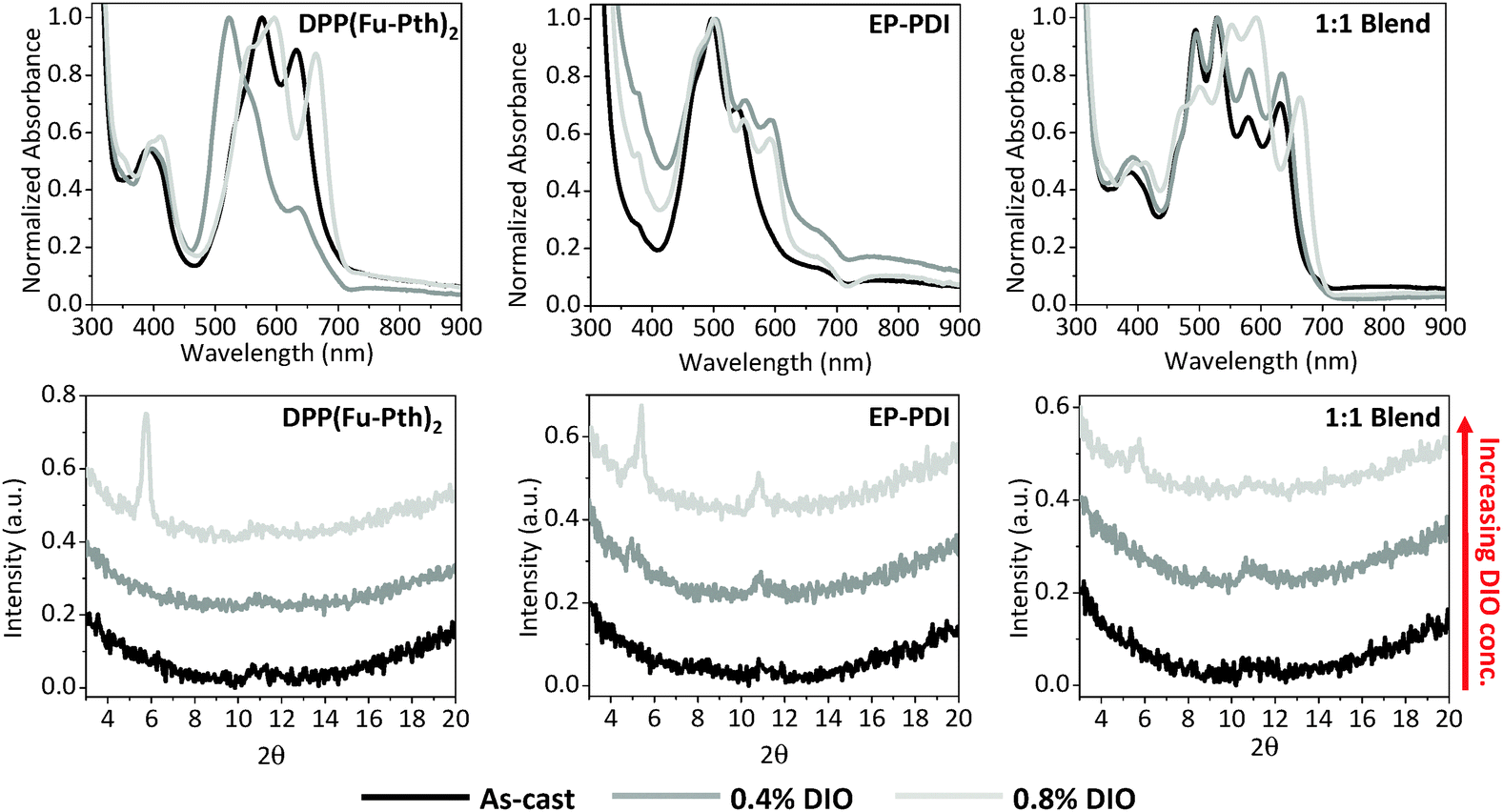 | ||
| Fig. 8 UV-vis absorption spectra (upper raw) and XRD patterns (lower raw) of neat and 1:1 DPP(Fu-Pth)2:EP-PDI blend films. | ||
 | ||
| Fig. 9 AFM height mode images (5 μm × 5 μm) of neat and blend films cast from CHCl3 solutions of different DIO concentrations. | ||
Since the use of DIO induces morphological changes as characterized by the emergence of diffraction peaks, the impact of DIO concentration on the morphology of the neat and blend films was measured using AFM as shown in Fig. 9. As the DIO content in the casting solution is increased, the surface roughness of DPP(Fu-Pth)2 films increases progressively with larger surface features. The EP-PDI films cast with 0.4% DIO have smaller features than the neat films, which become larger upon further increase in the DIO concentration.
For the blend films, the addition of 0.4% DIO eliminates the formation of large aggregates and results in the formation of needle-shaped crystallites between 0.3 and 1.0 μm in length. Doubling the concentration of DIO additive produces a film of flake-like crystallites. The single diffraction peak at 5.7° suggests that the flake-like structures are crystalline domains of DPP(Fu-Pth)2.
F. Photovoltaic performance
Considering the three different processing techniques studied so far, none of them promoted an idealized active layer morphology, which is necessary to achieve high PCE. The use of DIO as a solvent additive resulted in the smallest domain size compared to the annealing techniques, which might be considered the most appropriate methodology to fabricate the active layer of OPV devices. In this respect, a conventional BHJ architecture (Fig. 10A) was used to examine the effect of DIO on performance as an active layer in OPV cells. The architectures are as follows: ITO/PEDOT:PSS/1:1 blend films/Ca/Al. Current–voltage curves of selected devices are presented in Fig. 10. As-cast devices showed no appreciable PV response. Although inclusion of small volume fractions of DIO in the blends increased the open circuit voltage (Voc) from 0 for the as-cast devices to 0.54 and 0.77 V for those with the active layer spun from solutions containing 0.2 and 0.4 v/v% DIO, respectively, however, the large domain size compared to exciton diffusion lengths diminishes charge separation, and thus the photovoltaic (PV) performance is still almost zero. At higher DIO loading (0.6%), the short circuit current (Jsc) is increased dramatically to 0.093 mA cm−2 (Voc 0.78, fill factor (FF) 0.43 and PCE 0.032%). This could be explained by the improved film crystallinity as confirmed from the XRD measurements (Fig. 8). This suggests the onset of percolating pathways throughout the blend film, which enables charge collection at the electrodes.
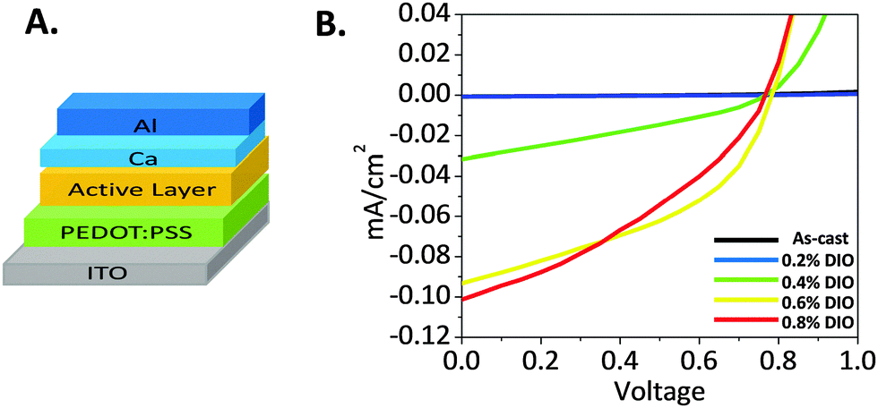 | ||
| Fig. 10 (A). Conventional BHJ device architecture. (B) Current–voltage curves of the 1:1 DPP(Fu-Pth)2:EP-PDI blend film based devices spun from DIO containing solutions. | ||
Conclusions
The morphology of a BHJ blend film comprised of potential donor and acceptor materials, viz. DPP(Fu-Pth)2 and EP-PDI for OPV applications, have been tuned via post-production thermal and solvent annealing as well as the usage of solvent additives. The results indicated that both annealing techniques led to the comparable optical properties and self-assembly of two compounds in blend, which were quite different when the active layer was processed using DIO as a solvent additive. Although the three processing techniques did not yield the optimal morphology for BHJ solar cells, PV measurements indicated that the active layer processed in the presence of DIO has a reasonable Voc (0.78 V) and low Jsc (0.093 mA cm−2). This suggests that further processing optimization is necessary to reduce the domain size to achieve ultimately an effective charge separation and high PCE. Moreover, the tendency of the small molecules for over crystallization in solid films should lay down new guidelines (other than decreasing the molecular planarity) for synthetic chemists when designing new materials that take into consideration not only electronic properties and film forming ability of the new materials, but also their tendency for self-assembly.Acknowledgements
AFE thanks Arthur D. Hendsbee from University of Calgary for acquiring and analysing the CV data of EP-PDI. GCW acknowledges NSERC Discovery Grants Program, CFI John Evans Leadership Fund, Canada Research Chairs Program, and the University of Calgary. AN is grateful for a NSERC CGS scholarship and DREAMS sponsorship. IGH acknowledges NSERC Discovery Grants Program.References
- J. Jean, P. R. Brown, R. L. Jaffe, T. Buonassisi and V. Bulovic, Energy Environ. Sci., 2015, 8, 1200–1219 CAS
.
- R. Søndergaard, M. Hösel, D. Angmo, T. T. Larsen-Olsen and F. C. Krebs, Mater. Today, 2012, 15, 36–49 CrossRef
- M. Kaltenbrunner, M. S. White, E. D. Głowacki, T. Sekitani, T. Someya, N. S. Sariciftci and S. Bauer, Nat. Commun., 2012, 3, 770 CrossRef PubMed
- T. R. Andersen, H. F. Dam, M. Hosel, M. Helgesen, J. E. Carle, T. T. Larsen-Olsen, S. A. Gevorgyan, J. W. Andreasen, J. Adams, N. Li, F. Machui, G. D. Spyropoulos, T. Ameri, N. Lemaitre, M. Legros, A. Scheel, D. Gaiser, K. Kreul, S. Berny, O. R. Lozman, S. Nordman, M. Valimaki, M. Vilkman, R. R. Sondergaard, M. Jorgensen, C. J. Brabec and F. C. Krebs, Energy Environ. Sci., 2014, 7, 2925–2933 CAS
- W. Cao and J. Xue, Energy Environ. Sci., 2014, 7, 2123–2144 CAS
- K. A. Mazzio and C. K. Luscombe, Chem. Soc. Rev., 2015, 44, 78–90 RSC
- A. F. Eftaiha, J.-P. Sun, I. G. Hill and G. C. Welch, J. Mater. Chem. A, 2014, 2, 1201–1213 CAS
- B. C. Thompson and J. M. J. Fréchet, Angew. Chem., Int. Ed., 2008, 47, 58–77 CrossRef CAS PubMed
- Y.-J. Cheng, S.-H. Yang and C.-S. Hsu, Chem. Rev., 2009, 109, 5868–5923 CrossRef CAS PubMed
- J. Yan and B. R. Saunders, RSC Adv., 2014, 4, 43286–43314 RSC
- A.-J. Payne and G. C. Welch, Mater. Matters, 2014, 9, 23–27 CAS
- S. M. McAfee, J. M. Topple, I. G. Hill and G. C. Welch, J. Mater. Chem. A, 2015, 3, 16393–16408 CAS
- J. Roncali, Acc. Chem. Res., 2009, 42, 1719–1730 CrossRef CAS PubMed
- Y. Lin, Y. Li and X. Zhan, Chem. Soc. Rev., 2012, 41, 4245–4272 RSC
- T. Liu and A. Troisi, Adv. Mater., 2013, 25, 1038–1041 CrossRef CAS PubMed
- Y. Sun, G. C. Welch, W. L. Leong, C. J. Takacs, G. C. Bazan and A. J. Heeger, Nat. Mater., 2012, 11, 44–48 CrossRef CAS PubMed
- J. Zhou, X. Wan, Y. Liu, Y. Zuo, Z. Li, G. He, G. Long, W. Ni, C. Li, X. Su and Y. Chen, J. Am. Chem. Soc., 2012, 134, 16345–16351 CrossRef CAS PubMed
- O. K. Kwon, J.-H. Park, D. W. Kim, S. K. Park and S. Y. Park, Adv. Mater., 2015, 27, 1951–1956 CrossRef CAS PubMed
- A. K. K. Kyaw, D. H. Wang, D. Wynands, J. Zhang, T.-Q. Nguyen, G. C. Bazan and A. J. Heeger, Nano Lett., 2013, 13, 3796–3801 CrossRef CAS PubMed
- B. Kan, Q. Zhang, M. Li, X. Wan, W. Ni, G. Long, Y. Wang, X. Yang, H. Feng and Y. Chen, J. Am. Chem. Soc., 2014, 136, 15529–15532 CrossRef CAS PubMed
- J. Zhou, Y. Zuo, X. Wan, G. Long, Q. Zhang, W. Ni, Y. Liu, Z. Li, G. He, C. Li, B. Kan, M. Li and Y. Chen, J. Am. Chem. Soc., 2013, 135, 8484–8487 CrossRef CAS PubMed
- Y. Lin, J. Wang, Z.-G. Zhang, H. Bai, Y. Li, D. Zhu and X. Zhan, Adv. Mater., 2015, 27, 1170–1174 CrossRef CAS PubMed
- D. Sun, D. Meng, Y. Cai, B. Fan, Y. Li, W. Jiang, L. Huo, Y. Sun and Z. Wang, J. Am. Chem. Soc., 2015, 137, 11156–11162 CrossRef CAS PubMed
- M. A. Naik and S. Patil, J. Polym. Sci., Part A: Polym. Chem., 2013, 51, 4241–4260 CrossRef CAS
- Y. Li, P. Sonar, L. Murphy and W. Hong, Energy Environ. Sci., 2013, 6, 1684–1710 CAS
- S. Qu and H. Tian, Chem. Commun., 2012, 48, 3039–3051 RSC
- C. B. Nielsen, M. Turbiez and I. McCulloch, Adv. Mater., 2013, 25, 1859–1880 CrossRef CAS PubMed
- A. B. Tamayo, M. Tantiwiwat, B. Walker and T.-Q. Nguyen, J. Phys. Chem. C, 2008, 112, 15543–15552 CAS
- M. Tantiwiwat, A. Tamayo, N. Luu, X.-D. Dang and T.-Q. Nguyen, J. Phys. Chem. C, 2008, 112, 17402–17407 CAS
- B. Walker, A. B. Tamayo, X.-D. Dang, P. Zalar, J. H. Seo, A. Garcia, M. Tantiwiwat and T.-Q. Nguyen, Adv. Funct. Mater., 2009, 19, 3063–3069 CrossRef CAS
- B. Walker, X. Han, C. Kim, A. Sellinger and T.-Q. Nguyen, ACS Appl. Mater. Interfaces, 2011, 4, 244–250 Search PubMed
- O. V. Mikhnenko, J. Lin, Y. Shu, J. E. Anthony, P. W. M. Blom, T.-Q. Nguyen and M. A. Loi, Phys. Chem. Chem. Phys., 2012, 14, 14196–14201 RSC
- C. Kim, J. Liu, J. Lin, A. B. Tamayo, B. Walker, G. Wu and T.-Q. Nguyen, Chem. Mater., 2012, 24, 1699–1709 CrossRef CAS
- J. Liu, B. Walker, A. Tamayo, Y. Zhang and T.-Q. Nguyen, Adv. Funct. Mater., 2013, 23, 47–56 CrossRef CAS
- J. D. A. Lin, J. Liu, C. Kim, A. B. Tamayo, C. M. Proctor and T.-Q. Nguyen, RSC Adv., 2014, 4, 14101–14108 RSC
-
S. McAfee, G. C. Welch and C. V. Hoven, Polymer Photovoltaics: Materials, Physics, and Device Engineering, The Royal Society of Chemistry, 2016, pp. 127–178 Search PubMed
- J. W. Ryan and Y. Matsuo, Sci. Rep., 2015, 5, 8319 CrossRef CAS PubMed
- J. W. Jung and W. H. Jo, Chem. Mater., 2015, 27, 6038–6043 CrossRef CAS
- L. R. Rutledge, S. M. McAfee and G. C. Welch, J. Phys. Chem. A, 2014, 118, 7939–7951 CrossRef CAS PubMed
- S. M. McAfee, J. M. Topple, A.-J. Payne, J.-P. Sun, I. G. Hill and G. C. Welch, ChemPhysChem, 2015, 16, 1190–1202 CrossRef CAS PubMed
- A. D. Hendsbee, J.-P. Sun, L. R. Rutledge, I. G. Hill and G. C. Welch, J. Mater. Chem. A, 2014, 2, 4198–4207 CAS
- C. H. Woo, P. M. Beaujuge, T. W. Holcombe, O. P. Lee and J. M. J. Fréchet, J. Am. Chem. Soc., 2010, 132, 15547–15549 CrossRef CAS PubMed
- A. D. Hendsbee, J.-P. Sun, T. M. McCormick, I. G. Hill and G. C. Welch, Org. Electron., 2015, 18, 118–125 CrossRef CAS
- J. Areephong, A. D. Hendsbee and G. C. Welch, New J. Chem., 2015, 39, 6714 RSC
- J. E. Anthony, Chem. Mater., 2011, 23, 583–590 CrossRef CAS
- E. Kozma and M. Catellani, Dyes Pigm., 2013, 98, 160–179 CrossRef CAS
- S. Rajaram, R. Shivanna, S. K. Kandappa and K. S. Narayan, J. Phys. Chem. Lett., 2012, 3, 2405–2408 CrossRef CAS PubMed
- X. Zhang, Z. Lu, L. Ye, C. Zhan, J. Hou, S. Zhang, B. Jiang, Y. Zhao, J. Huang, S. Zhang, Y. Liu, Q. Shi, Y. Liu and J. Yao, Adv. Mater., 2013, 25, 5791–5797 CrossRef CAS PubMed
- Y. Zang, C.-Z. Li, C.-C. Chueh, S. T. Williams, W. Jiang, Z.-H. Wang, J.-S. Yu and A. K.-Y. Jen, Adv. Mater., 2014, 26, 5708–5714 CrossRef CAS PubMed
- L. Ye, K. Sun, W. Jiang, S. Zhang, W. Zhao, H. Yao, Z. Wang and J. Hou, ACS Appl. Mater. Interfaces, 2015, 7, 9274–9280 CAS
- P. E. Hartnett, A. Timalsina, H. S. S. R. Matte, N. Zhou, X. Guo, W. Zhao, A. Facchetti, R. P. H. Chang, M. C. Hersam, M. R. Wasielewski and T. J. Marks, J. Am. Chem. Soc., 2014, 136, 16345–16356 CrossRef CAS PubMed
- A. Sharenko, C. M. Proctor, T. S. van der Poll, Z. B. Henson, T.-Q. Nguyen and G. C. Bazan, Adv. Mater., 2013, 25, 4403–4406 CrossRef CAS PubMed
- A. Sharenko, D. Gehrig, F. Laquai and T.-Q. Nguyen, Chem. Mater., 2014, 26, 4109–4118 CrossRef CAS
- M. Li, J. Liu, X. Cao, K. Zhou, Q. Zhao, X. Yu, R. Xing and Y. Han, Phys. Chem. Chem. Phys., 2014, 16, 26917–26928 RSC
- Y. Liu, C. Mu, K. Jiang, J. Zhao, Y. Li, L. Zhang, Z. Li, J. Y. L. Lai, H. Hu, T. Ma, R. Hu, D. Yu, X. Huang, B. Z. Tang and H. Yan, Adv. Mater., 2015, 27, 1015–1020 CrossRef CAS PubMed
- T. Wang, A. J. Pearson, D. G. Lidzey and R. A. L. Jones, Adv. Funct. Mater., 2011, 21, 1383–1390 CrossRef CAS
- E. Verploegen, C. E. Miller, K. Schmidt, Z. Bao and M. F. Toney, Chem. Mater., 2012, 24, 3923–3931 CrossRef CAS
- H.-C. Liao, C.-C. Ho, C.-Y. Chang, M.-H. Jao, S. B. Darling and W.-F. Su, Mater. Today, 2013, 16, 326–336 CrossRef CAS
- A. J. Heeger, Adv. Mater., 2014, 26, 10–28 CrossRef CAS PubMed
- Y. Chen, A. Tang, X. Zhang, Z. Lu, J. Huang, C. Zhan and J. Yao, J. Mater. Chem. A, 2014, 2, 1869–1876 CAS
- J. Huang, X. Wang, X. Zhang, Z. Niu, Z. Lu, B. Jiang, Y. Sun, C. Zhan and J. Yao, ACS Appl. Mater. Interfaces, 2014, 6, 3853–3862 CAS
- G. Marino, J. Heterocycl. Chem., 1972, 9, 817–819 CrossRef CAS
- X. Zhang, J. P. Johnson, J. W. Kampf and A. J. Matzger, Chem. Mater., 2006, 18, 3470–3476 CrossRef CAS
- J. Li, F. Dierschke, J. Wu, A. C. Grimsdale and K. Mullen, J. Mater. Chem., 2006, 16, 96–100 RSC
- J. D. Douglas, M. S. Chen, J. R. Niskala, O. P. Lee, A. T. Yiu, E. P. Young and J. M. J. Fréchet, Adv. Mater., 2014, 26, 4606 CrossRef CAS
- C. Nasr, T. Taleb, R. M. Leblanc and S. Hotchandani, Appl. Phys. Lett., 1996, 69, 1823–1825 CrossRef CAS
- Y. Terao, H. Sasabe and C. Adachi, Appl. Phys. Lett., 2007, 90, 103515 CrossRef
-
P. Würfel, Physics of Solar Cells: From Basic Principles to Advanced Concepts, Willey-VCH Verlag GmbH & Co., KGaA, Weinheim, 2009 Search PubMed
- R. R. Lunt, J. B. Benziger and S. R. Forrest, Adv. Mater., 2010, 22, 1233–1236 CrossRef CAS PubMed
- P. Sonar, J. P. Fong Lim and K. L. Chan, Energy Environ. Sci., 2011, 4, 1558–1574 CAS
- M. T. Dang and J. D. Wuest, Chem. Soc. Rev., 2013, 42, 9105–9126 RSC
- H.-C. Liao, C.-S. Tsao, Y.-C. Huang, M.-H. Jao, K.-Y. Tien, C.-M. Chuang, C.-Y. Chen, C.-J. Su, U.-S. Jeng, Y.-F. Chen and W.-F. Su, RSC Adv., 2014, 4, 6246–6253 RSC
- K. Sun, Z. Xiao, E. Hanssen, M. F. G. Klein, H. H. Dam, M. Pfaff, D. Gerthsen, W. W. H. Wong and D. J. Jones, J. Mater. Chem. A, 2014, 2, 9048–9054 CAS
- S. Grob, A. N. Bartynski, A. Opitz, M. Gruber, F. Grassl, E. Meister, T. Linderl, U. Hormann, C. Lorch, E. Moons, F. Schreiber, M. E. Thompson and W. Brutting, J. Mater. Chem. A, 2015, 3, 15700–15709 CAS
- A. Viterisi, F. Gispert-Guirado, J. W. Ryan and E. Palomares, J. Mater. Chem., 2012, 22, 15175–15182 RSC
- T. Salim, L. H. Wong, B. Brauer, R. Kukreja, Y. L. Foo, Z. Bao and Y. M. Lam, J. Mater. Chem., 2011, 21, 242–250 RSC
- J. Peet, N. S. Cho, S. K. Lee and G. C. Bazan, Macromolecules, 2008, 41, 8655–8659 CrossRef CAS
- A. K. K. Kyaw, D. H. Wang, C. Luo, Y. Cao, T.-Q. Nguyen, G. C. Bazan and A. J. Heeger, Adv. Energy Mater., 2014, 4, 1301469 Search PubMed
- W. Shin, T. Yasuda, G. Watanabe, Y. S. Yang and C. Adachi, Chem. Mater., 2013, 25, 2549–2556 CrossRef CAS
Footnote |
| † Electronic supplementary information (ESI) available. See DOI: 10.1039/c6cp01269h |
| This journal is © the Owner Societies 2016 |