 Open Access Article
 This Open Access Article is licensed under a Creative Commons Attribution-Non Commercial 3.0 Unported Licence
Band gap expansion, shear inversion phase change behaviour and low-voltage induced crystal oscillation in low-dimensional tin selenide crystals†
Robin
Carter
a,
Mikhail
Suyetin
b,
Samantha
Lister
c,
M. Adam
Dyson
d,
Harrison
Trewhitt
d,
Sanam
Goel
d,
Zheng
Liu
e,
Kazu
Suenaga
e,
Cristina
Giusca
f,
Reza J.
Kashtiban
d,
John L.
Hutchison
a,
John C.
Dore
c,
Gavin R.
Bell
d,
Elena
Bichoutskaia
*b and
Jeremy
Sloan
*d
aDepartment of Materials, University of Oxford, South Parks Road, Oxford, OX1 3PH, UK
bSchool of Chemistry, University of Nottingham, University Park, Nottingham, NG7 2RD, UK. E-mail: Elena.Bichoutskaia@nottingham.ac.uk
cSchool of Physical Sciences, Ingram Building and , University of Kent, Canterbury, Kent CT2 7NH, UK
dDepartment of Physics, University of Warwick, Coventry, Warwickshire CV4 7AL, UK. E-mail: j.sloan@warwick.ac.uk; Fax: +44 (0)24766 92016; Tel: +44 (0)24765 23392
eNanotube Research Center, National Institute of Advanced Industrial Science and Technology (AIST), Higashi 1-1-1, Tsukuba, 305-8565, Japan
fNational Physical Laboratory, Hampton Road, Teddington, TW11 0LW, UK
First published on 7th March 2014
Abstract
In common with rocksalt-type alkali halide phases and also semiconductors such as GeTe and SnTe, SnSe forms all-surface two atom-thick low dimensional crystals when encapsulated within single walled nanotubes (SWNTs) with diameters below ∼1.4 nm. Whereas previous density functional theory (DFT) studies indicate that optimised low-dimensional trigonal HgTe changes from a semi-metal to a semi-conductor, low-dimensional SnSe crystals typically undergo band-gap expansion. In slightly wider diameter SWNTs (∼1.4–1.6 nm), we observe that three atom thick low dimensional SnSe crystals undergo a previously unobserved form of a shear inversion phase change resulting in two discrete strain states in a section of curved nanotube. Under low-voltage (i.e. 80–100 kV) imaging conditions in a transmission electron microscope, encapsulated SnSe crystals undergo longitudinal and rotational oscillations, possibly as a result of the increase in the inelastic scattering cross-section of the sample at those voltages.
1. Introduction
For some years, the crystallography of low-dimensional crystals embedded within single-walled carbon nanotubes (SWNTs), and similar nanotubular structures has been investigated.1,2 When the diameters of the host tubules are reduced to the range 0.8–1.6 nm, embedded nanocrystals with sterically and systematically reduced coordination are observed resulting, in some instances, in metastable low-dimensional crystalline forms not encountered in the bulk forms of the same material.3,4 These behaviours are all cardinal illustrations of the so-called ‘confinement effect’5 widely reported for the changes in structure–physical properties of materials embedded within other templating structures such as zeolites,6 mesoporous phases,7 anodic alumina,8 metal organic framework (MOF)-type materials9 and similar. Reduced coordination crystals embedded within SWNTs in particular present a unique opportunity for investigating not only crystallographic changes in these materials as a function of nanoscale volume constraints but also any atomically regulated changes in low-dimensional physical properties that occur in tandem. The synthesis of such composites is now becoming scalable due to the fact that the host SWNTs can be grown and purified with increasing selectivity in terms of both their diameter and their electronic characteristics (e.g. all semiconducting vs. all metallic SWNTs with increasingly selective chiral vectors).10,11 At the same time the cross-sectional crystal structures of the confined crystals are regulated with associated precision due to the close relationship between the SWNT chiral vector and its confining van der Waals surface.1 Given that the resulting crystals are merely 2–3 atoms thick in cross-section,1,12 investigations into their structure–physical properties may inform developments in nanoscale devices formed on this scale for years to come and possibly also lead to the incorporation of 1D crystal composites into such devices. The associated changes in physical properties may also lead to many exciting new challenges and opportunities.Density functional theory (DFT) type investigations and experimental investigations indicate that SWNT-embedded crystals,4,13–15 including p-type (electron donor) embedded iodine16,17 and, more recently, embedded graphene ribbons18,19 are all profoundly modified with regards to their corresponding bulk properties. Additionally, a combination of theoretical and experimental approaches have demonstrated that n-type (electron acceptor) properties exist for SWNT embedded, for example, with zinc,20 copper21 and cadmium22 halides. Charge-transfer behaviour between SWNTs and molecular scale species (i.e. such as these crystals) and single molecules or molecular scale ions23 is strongly correlated with local perturbations in the densities of states (DOS) of the encapsulating SWNTs although at least of comparable interest are the fundamental changes predicted to occur in the physical characteristics of embedded low-dimensional crystals. For example, we have reported band-gap ‘flipping’ for low-dimensional ‘tubular’ HgTe embedded within 1.35–1.49 nm diameter SWNTs4,15 and, most recently, we have demonstrated that SWNT embedded GeTe crystals exhibit unprecedented phase change behaviour on the smallest possible scale.24 In the present investigation, we describe structural and theoretical investigations into low-dimensional crystals of SnSe. Like many metal chalcogenides, confined thin films of SnSe have long exhibited significant potential in optoelectronic applications such as holographic recording systems25 and solar cells.26 Of particular interest in the current study is how this material, which typically exhibits the orthorhombic Pnma form in the bulk27 (Fig. 1, top), but which also forms a Fm![[3 with combining macron]](https://www.rsc.org/images/entities/char_0033_0304.gif) m rocksalt form (Fig. 2, bottom) under high pressure or thin film epitaxy growth conditions28 responds to confinement in a narrower class of SWNTs (i.e. diameter <1.4 nm). Bulk SnSe has an indirect band gap of 0.90 eV and a direct band gap of 1.30 eV.29 In addition to exploring any changes in local crystal structure we also wished to explore how this material would interact with the encapsulating tubules in terms of the composite physical properties.
m rocksalt form (Fig. 2, bottom) under high pressure or thin film epitaxy growth conditions28 responds to confinement in a narrower class of SWNTs (i.e. diameter <1.4 nm). Bulk SnSe has an indirect band gap of 0.90 eV and a direct band gap of 1.30 eV.29 In addition to exploring any changes in local crystal structure we also wished to explore how this material would interact with the encapsulating tubules in terms of the composite physical properties.
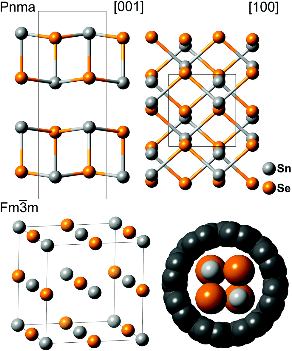 | ||
| Fig. 1 (Top) [001] and [100] ball-and-stick representations of the layered orthorhombic Pnma form of SnSe (for unit cell data, see Table 1). (Bottom left) Perspective view of the Fmm rocksalt form of SnSe. (Bottom right) Space-filling representation of and undistorted 2 × 2 crystal fragment derived from the Fmm form within an (8,8) SWNT. | ||
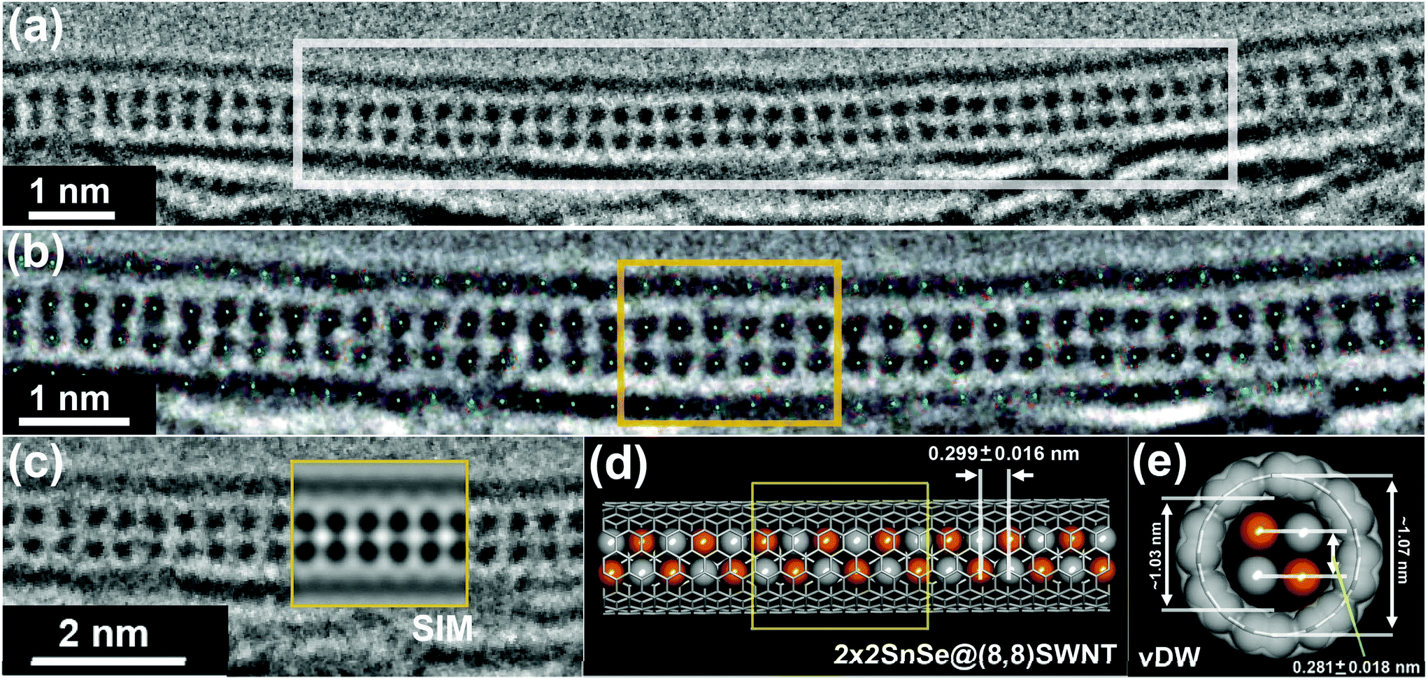 | ||
| Fig. 2 (a) AC-TEM image of a (2 × 2)SnSe@SWNT composite with clearly resolved image contrast and perfect ordering for Sn–Se atom column pairs arranged along a ∼20 nm section of a ∼1.1 nm diameter SWNT. (b) Enlargement of the white box region in (a) with blue dots indicating the centres of the Sn–Se columns relative to the SWNT wall. The yellow boxed region was used to provide the initial atomic position dataset for the subsequent DFT optimisations. (c) Second enlargement from (a) but with overlaid AC-TEM multislice image simulation (SIM) and atom positions refined from the (2 × 2 × 6)SnSe@(8,8)SWNT DFT optimisation. (d) Side on view of the experimental model indicating the statistically determined lattice spacing along the SWNT. (e) As (d) but in end-on view and with the relative dimensions of the encapsulating SWNT indicated and also the statistical lattice spacing indicated across the SWNT. The precision of this measurement was found to be slightly lower than in (d) due to lateral oscillation of the SnSe crystal (vide infra). A van der Waals (vDW) surface is added to the SWNT wall in this model. | ||
2. Experimental section
2.1. Synthesis of SnSe@SWNT composites
The single walled carbon nanotubes used in these experiments were all prepared by the technique of catalytically-assisted Krätschmer–Huffman electric arc vapourisation. Two grades of such tubes were utilised in this study, arc-grown and pre-purified SWNTs produced by NanoCarbLab and then so-called NI96 (commercial name ‘PureTubes’) purified and supplied by NanoIntegris. Both grades of nanotubes were filled by the modified high yield molten-phase capillarity technique adapted for SnSe filling. SWNTs were intimately ground with SnSe (99.995%, Sigma Aldrich), heated in pure silica quartz tubes sealed under vacuum to 100 °C above the melting point of SnSe (m.p. 861 °C, i.e. ∼960 °C), thermally cycled according to a published high-filling yield protocol30 and the composite was then allowed to cool down slowly to room temperature. For Aberration Corrected High Resolution Transmission Electron Microscopy (AC-TEM) studies of SnSe@SWNT composites, ∼1–2 mg-scale quantities of the filled nanotubes were typically dispersed ultrasonically in ∼3 ml of AnalaR® grade ethanol using a 750 W sonic horn operated at 20% power with 2 s on/off pulsing for 10 min before drop casting onto 3.05 mm Agar lacy carbon coated Cu support grids.2.2. AC-TEM of SnSe@SWNT composites
Initial AC-TEM images were obtained at 100 kV using a JEOL 2010F transmission electron microscope equipped with a CEOS aberration corrector for which Cs was tuned to ∼0.001 mm. Additional AC-TEM images were obtained at 80 kV were obtained on a JEOL JEM-ARM200F equipped with an imaging corrector for which Cs was also tuned to ∼0.001 mm. Direct measurements on lattice images were performed with the commercially available Gatan Digital Micrograph Suite 2.02 software and further analyzed with in-house written scripts. Structure models were assembled using CrystalMaker (Version 8) software and standard Shannon anion and cation radii. Nanotube models for the composite models and AC-TEM simulations were produced using Nanotube Modeler from JCrystalSoft (©2005–2013). Image simulations were performed from density functional theory (DFT) refined structural data using the multislice package SimulaTEM.2.3. DFT modelling of SnSe@SWNT composites
In this work, we performed DFT modelling and used refined atomic coordinates obtained from these calculations as input for AC-TEM simulations (above) but also to make predictions about the discrete and composite densities of states (DOS) of both isolated (in vacuo) and composite (i.e. with (n,m) conformation SWNTs) SnSe nanorods, respectively. The optimised bulk forms of SnSe (i.e. both Pnma and Fmm) and various composites of infinite and 2 × 2 × 6 atomic layer SnSe nanorods and (7,7) and (8,8) SWNTs were computed using the PW91 functional with dispersion correction as implemented in the CASTEP program,31 utilizing periodic boundary conditions. Ultra-soft pseudopotentials for the core electrons of the atoms were generated ‘on-the-fly’ using CASTEP. In all calculations, an energy cutoff of 600 eV was used and, in the case of the Pnma and Fmm bulk forms of SnSe, the Brillouin zones were sampled with 9 k-points and 4 k-points respectively. Due to the relatively larger size of their respective unit cells, the Brillouin zones of the SnSe nanorods and the nanorod/SWNT composites were sampled with one k-point only.
3. Electron microscopy studies and DFT modelling of undistorted encapsulated 2 × 2 SnSe crystals
3.1. AC-TEM imaging of undistorted 2 × 2 SnSe crystals
Inside the narrower diameter range 1–1.4 nm NanoCarbLab SWNTs, we observed a preponderance of bilayer 2 × 2 SnSe nanocrystals (Fig. 2(a)–(e)), although we briefly reported such crystals formed within comparable diameter arc-grown SWNTs.32 In this previous study, restored exit-wave imaging revealed a 2 × 2 ‘ladder’-like structure in which alternating pairs of Sn–Se atom columns were separated by 0.28 nm and 0.37 nm respectively, presumably as a result of the 2 × 2 crystal being rotated a few degrees about the axis relative to an ideal <001> projection defined according to an imaginary 2 × 2 ‘rocksalt’ SnSe unit cell. Alternatively, there exists the possibility that this structure may be distorted significantly with respect to an ideal rocksalt 2 × 2 microstructure as we have previously reported for encapsulated 2 × 2 KI crystals and similar1,12,33 although we may further anticipate structural distortions as a consequence of competition between the ‘ideal’ rocksalt 2 × 2 form and one derived from a more distorted Pnma form (Fig. 1). Any observable distortions may give significant insights into what can cause phase change behaviour as we have previously noted for similar-sized GeTe nanocrystals which can reversibly transform from a 2 × 2 form to an amorphous microstructure.24 It should also be noted that in the previous study,32 comparatively high electron accelerating voltages were used (i.e. 300 kV versus 100 kV and 80 kV in the present study) which may cause significant knock-on damage to the encapsulating SWNT, possibly resulting in distortions to the encapsulated microstructure.34In the present study we note that numerous individual images of the 2 × 2 SnSe nanocrystals are obtained with the crystal viewed parallel to <001> relative to an ideal 2 × 2 rocksalt structure (e.g.Fig. 2(a)–(c)). Systematic measurements of the lateral spacings of these encapsulated SnSe nanorods (Fig. 2(b)) relative to the centre point of the SWNT wall indicate that the obtained microstructure is undistorted and does not deviate significantly from the idealised 2 × 2 structure in spite of some mild curvature in the SWNT and d<200> lattice spacings (i.e. defined relative to the rocksalt SnSe, see also Table 1) measured along the SWNT corresponded to 0.299 nm (±0.014 nm), consistent with d<200> for rocksalt SnSe.28 However, as we discuss further below induced lateral and rotational oscillation of the encapsulated SnSe nanocrystal in response to 80 keV electrons reduced the relative precision of lateral d<020> measurements to 0.28 ± 0.01 nm.
m forms of SnSe. The nearest Sn–Se separation for the latter is indicated for both cases
| Parameter | Pnma |
Fmm |
||
|---|---|---|---|---|
| Calc. | Exp. | Calc. | Exp. | |
| a (nm) | 1.166 | 1.150 | 0.603 | 0.599 |
| b (nm) | 0.420 | 0.415 | 0.603 | 0.599 |
| c (nm) | 0.447 | 0.445 | 0.603 | 0.599 |
| α (°) | 90 | 90 | 90 | 90 |
| β (°) | 90 | 90 | 90 | 90 |
| γ (°) | 90 | 90 | 90 | 90 |
| Sn⋯Se (nm) | 0.300 | 0.302 | ||
3.2. DFT modelling of bulk and encapsulated SnSe
In order to study the effect of SnSe confinement and in order to accurately model the experimental SnSe@SWNT composite, we have modelled both bulk forms of SnSe and both finite and infinite SnSe nanorods in vacuo in order to test the efficiency of our optimisations. We then tested the effect of SWNT confinement in two armchair conformation SWNTs (i.e. (7,7) and (8,8))35 and then computed the densities of states (DOS) for the infinite and optimised 2 × 2 × 6 SnSe cases respectively.Calculated and experimentally determined lattice parameters for the orthorhombic Pnma and cubic Fmm forms of SnSe are reproduced in Table 1. The computed lattice parameters for both bulk structures are in excellent agreement with experiment. In terms of the relative lattice energies of the Pnma and cubic Fmm SnSe forms, both compute with a marginally different energy (i.e. −1027.8121 eV for the rocksalt form versus −1027.7648 eV for the Pnma form, respectively) indicating that the latter is marginally more stable although is less commonly observed. In terms of the DOS (Fig. 4(a) and (b)), we find that the Pnma bulk SnSe form computes with a significantly wider band gap (i.e. 0.9 eV) in comparison to rocksalt SnSe (i.e. 0.68 eV) presumably as a result of the slightly more open structure.
As an initial input for the optimisation of the 2 × 2 SnSe microstructure, we utilised atomic coordinates estimated from a ∼10 nm long sub-domain of an extended lattice image of a 16 nm filled SWNT (i.e.Fig. 1(b)). Following preliminary calculations, we found that a 2 × 2 × 6 atomic rod of SnSe (Fig. 3(a), top) was sufficient to equilibrate the structure with a reasonable level of precision with the central Sn4Se4 cubic cluster optimising (in vacuo) with lateral and longitudinal Sn–Se distances equivalent to the experimental case (i.e.Fig. 1(d) and (e)). A further optimisation with an “infinite rod” crystal of SnSe was found to produce similar lateral and longitudinal Sn–Se distances within experimental error (Fig. 3(a), bottom).
 | ||
| Fig. 3 (a) Top model shows an optimisation of 2 × 2 × 6 Sn12Se12 rod using periodic boundary conditions and SnSe atom column positions initially determined from the yellow box in Fig. 2(b) as input data. Following optimisation, the bonds distort symmetrically around the central Sn4Se4 cluster (left bonds shown only). The bottom model shows a similar simulation but for an effectively infinite SnSe nanorod. Following optimisation, identical longitudinal and lateral Sn–Se bonds are obtained. (b) Effect on optimisation of central Sn4Se4 cluster following confinement in two different diameter but structural equivalent SWNTs (as per (c) and (d)). In the top case, the Sn4Se4 cluster is confined within a ∼0.95 nm diameter (7,7) SWNT and the lateral Sn–Se bonds (in yellow) are ‘compressed’ to 0.264 nm and this composite had a slightly positive encapsulation energy. The bottom Sn4Se4 cluster was optimised within a more accommodating ∼1.09 nm diameter (8,8) SWNT. In this instance, the lateral Sn–Se bonds (in green) do not significantly distort away from the equivalent bonds in (a) and this structure was obtained with a more favourable −3.019 eV encapsulation energy. (c) and (d) Perspective and end-on views of (2 × 2 × 6)SnSe@(7,7)SWNT and (2 × 2 × 6)SnSe@(8,8)SWNT composites, respectively. Atomic positions determined for the second case were used as input date for the multislice image simulation embedded in Fig. 1(c). | ||
We next observed the effect of SWNT confinement on the local geometry of the 2 × 2 × 6 SnSe rod in terms of the DFT optimisation. Fig. 3(b) shows two cases where the central Sn4Se4 cubic cluster in a 2 × 2 × 6 nanorod is optimised in a narrower ∼0.95 nm diameter (7,7) SWNT and then in a slightly wider ∼1.09 diameter (8,8) SWNT. In the first case (Fig. 3(b), top), the longitudinal Sn–Se distances optimise to 0.300 nm, comparable to similar Sn–Se distances in the central Sn4Se4 cubic cluster in the optimised 2 × 2 × 6 SnSe nanorod (Fig. 3(a), top) and also to those of Sn4Se4 units in the infinite SnSe nanorod (Fig. 3(a), bottom). However the lateral bond distances in the 2 × 2 × 6 SnSe rod optimised within the narrower (7,7) SWNT are found to be somewhat compressed to ∼0.264 nm in comparison either to the experimental case (i.e. 0.28 nm, Fig. 1(e)) or those determined for either of the optimisations in Fig. 3(a) (i.e. ∼0.275–0.277 nm). When the 2 × 2 × 6 nanorod is optimised in the slightly wider (8,8) SWNT (i.e.Fig. 3(b), bottom), longitudinal and lateral Sn–Se separations are obtained that are more compatible with both theory and experiment.
Together with the structural optimisations of the 2 × 2 × 6 SnSe nanorods we have computed comparisons between the 1D densities of states (DOS) for the finite and infinite cases in order to compare them against the two bulk forms. Computing the DOS for the bulk Pnma and Fmm forms in the first instance (Fig. 4(a)) reveals that the layered orthorhombic form has a wider 0.93 eV band gap than the 0.68 eV gap determined for cubic rocksalt form, which is a less open structure. Given that the 2 × 2 × 6 nanorod structure is more closely related to this more densely packed form of SnSe, we argue that the modification of the electronic structure should be seen within the context of this archetype. Computing the DOS for both the finite and infinite rod variants of (2 × 2) SnSe produces only comparatively small differences in the electronic structure (Fig. 4(b)) and a small difference in the band gap for the finite 2 × 2 × 6 SnSe nanorod (i.e. 1.41 eV) versus the band gap determined for the infinite SnSe nanorod (i.e. 1.36 eV). Both computed gaps represent a significant expansion of the band gap corresponding to the ‘parent’ Fmm form.
 | ||
| Fig. 4 (a) A comparison of the densities of states (DOS) for the two bulk forms of SnSe. Lamellar Pnma SnSe exhibits a wider band gap (i.e. 0.93 eV) in comparison to Fmm SnSe (0.68 eV). (b) DOS computed for finite (i.e. 2 × 2 × 6) rod SnSe as depicted in the top model in Fig. 3(a) overlaid on the DOS computed for an infinite (2 × 2) SnSe nanorod. In this instance there is only a marginal difference between the estimated band gap for the 2 × 2 × 6 case (i.e. 1.41 eV) versus that determined for the infinite form (i.e. 1.36 eV) while both exhibit a significantly expanded band gap relative to either of the bulk forms. | ||
In terms of the properties of the surrounding SWNTs, both (7,7) and (8,8) SWNTs must be expected to be metallic and these would no doubt shield or mask both the DOS and also the expanded band gap of the encapsulated SnSe crystals. On the other hand, exciting electron transfer in the latter would permit the metallic tubes to act as a conduit for electron transfer from the encapsulates to elsewhere which may have implications for sensor devices based on these and similar nanocomposites.
4. Electron beam induced strain and oscillation effects observed in encapsulated SnSe nanocrystals
4.1. Beam-induced shear inversion phase change behaviour in SnSe encapsulated in wider SWNTs
Encapsulating SnSe in nanotubes with median diameter ranges higher than the NanoCarboLab SWNTs might be expected to produce crystals with systematically and integrally expanded atomic layer thicknesses from (2 × 2) a series 3 × 3, 4 × 4⋯n × n as observed for certain alkali halides in variable diameter SWNTs.12 In fact 3 × 3 SnSe nanocrystals incorporated in only slightly wider (i.e. >1.4 nm diameter) NanoIntegris nanotubes were found to be significantly strained with apparently expanded, sheared and distorted lattice spacings relative to either 2 × 2 SnSe (Fig. 5(a)–(c) and insets). The reason for this may be related to the competition between the more compact Fmm-derived 2 × 2 form and the more open lamellar Pnma bulk structure which may tend to reform once the SWNTs diameters exceed ∼1.4 nm. The precise explanation may come down to a subtle interplay between the Sn![[thin space (1/6-em)]](https://www.rsc.org/images/entities/char_2009.gif) :Se radius ratios and the confining van der Waals internal surface of the encapsulating SWNT, an influence that we already show is critical in terms of stabilising or destabilising the 2 × 2 form in narrower ≤1 nm diameter SWNTs (i.e.Fig. 3(b)).
:Se radius ratios and the confining van der Waals internal surface of the encapsulating SWNT, an influence that we already show is critical in terms of stabilising or destabilising the 2 × 2 form in narrower ≤1 nm diameter SWNTs (i.e.Fig. 3(b)).
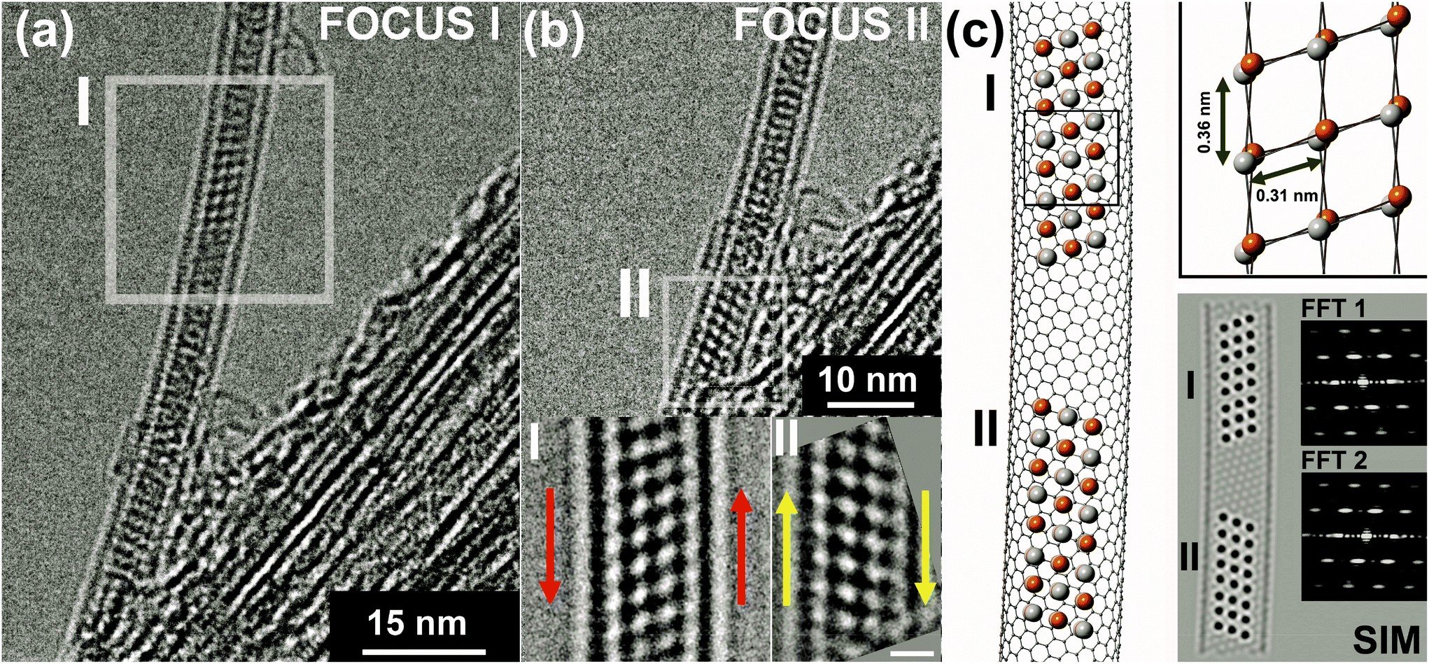 | ||
| Fig. 5 (a) First SnSe shear structure (I) in a ∼1.5 nm diameter curved SWNT obtained with the top section in focus. (b) Lower down in the same SWNT, a second shear structure (II) is observed at a different focus, indicating an overall tilt in the SWNT. The two insets at bottom show the relative shears of I and II (inset scale bar for II, 0.5 nm). These structures are significantly distorted relative to rocksalt SnSe (Fig. 1) and are apparently expanded but this may be due to staggering of the Sn and Se atoms. The two shear states I and II involve effectively 20° and −18° tilts away from an idealised (100) rocksalt lattice plane in a normal relationship to the SWNT axis. (c) Schematic model of shear inversion of I and II. Top right inset model indicates how staggering within the Sn and Se atom columns (observed within Pnma SnSe) can possibly lead to gross distortions in sheared rocksalt SnSe. Bottom right inset shows a multislice image simulation based on the main model. Fast Fourier transforms (FFTs) of shear structures I and II reveal mirror plane related diffraction behaviour which is useful in preferential dark field imaging techniques. | ||
A further consequence of these distortions is the observation of differential strain states insets that invert either side of a curve in a bent SWNT (i.e.Fig. 5(b) insets). This behaviour is similar though not identical to shearing behaviour that we reported for 3 × 3 AgI nanocrystals observed within ∼1.6 nm diameter SWNTs.36 In this case, the observed transformation was between rocksalt-like 3 × 3 AgI nanocrystals and a sheared version of this nanostructure. In the case of this new version of phase change behaviour, the process is shear inversion from one strain state (i.e. region I, Fig. 5(a)) to a second strain state (i.e. region II, Fig. 5(b)) that occurs either side of induced curvature in a SWNT in which the direction of shear is reversed (Fig. 5(b), inset and main model, Fig. 5(c)). The intermediate zone between the two sheared regions is filled with distorted and apparently amorphous SnSe. We note that this behaviour also differs from the recently reported electron beam induced crystalline-amorphous phase transitions in SWNT embedded GeTe nanocrystals.24
It is notable that both the shear states I and II inset in Fig. 5(b) involve small 20° and −18° distortions respectively relative to idealised 3 × 3 rocksalt fragments. This mode of shear inversion suggests a method for its automated identification if domains of similarly sheared nanocrystals can be induced in aligned bundles of SWNTs or similar. As shown in the inset in Fig. 5(c), a multislice image simulation (based on atomic coordinates extracted from strain states I and II in Fig. 5(b), inset) effectively reproduces the image contrast of the experimentally imaged shear inversion domains inset in Fig. 5(b). Fourier transforms of I and II produce two scattering patterns related by a mirror image. In real space dark field imaging, these patterns could be used to preferentially filter out either strain state allowing the other to be imaged selectively and dynamically, an effect that can also be reproduced offline digitally.
4.2. Beam-induced longitudinal, latitudinal and rotational oscillation observed in encapsulated SnSe nanocrystals
In addition to the strain effects that we describe above, all of the SnSe nanocrystals that we imaged at both 100 kV and 80 kV exhibited significant oscillations that could take either simple or more complex forms. This effect is not unique to SnSe and we have observed it in similar dimension SWNT-encapsulated nanocrystals observed at low voltages (e.g. TbCl3, KI, PbTe and similar) and other groups have reported related behaviour, prompting at least one group to attempt imaging crystal/nanotube composites on graphene.37In Fig. 6(a), we show two modes of beam-induced oscillation in another section of 2 × 2 SnSe encapsulated within a ∼1.1 nm diameter SWNT. The section of crystal on the right hand side of the SWNT behaves like an oscillating coiled spring with this domain of the crystal apparently expanding and contracting over the ∼12 s period of image acquisition. The left hand section of crystal exhibits a more complex mode of oscillation in that this entire region of crystal rotates about the axis of the SWNT, and the crystal rotates from a projection equivalent to <110> for rocksalt SnSe to <100>. In the former orientation (i.e. top three images in Fig. 6(a)), the crystal appears to have three layers but in fact, as the corresponding models and simulations in Fig. 6(b) show, the 2 × 2 fragment is being observed at a 45° rotation relative to the corresponding <100> orientation. An animation, including both the images included in Fig. 6(a) and other additional images from the same image sequence, reveals the nature of oscillational modes in more detail than is possible with static 2D images is reproduced in the ESI (i.e. Fig. S1†).
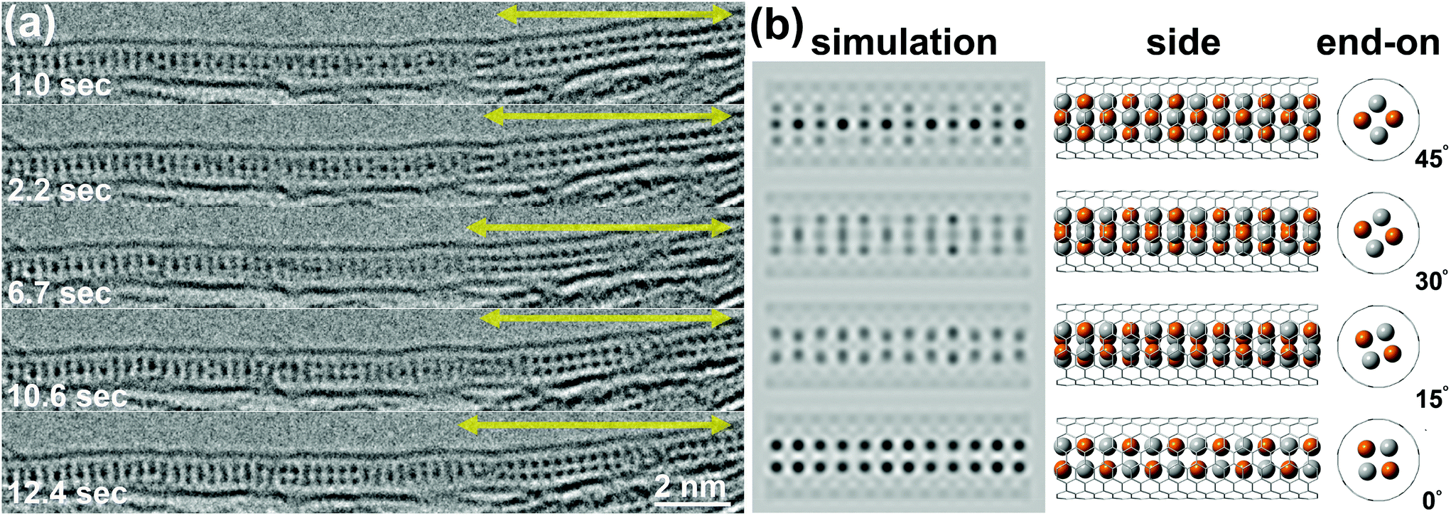 | ||
| Fig. 6 (a) This sequence of images obtained over ∼12 s at reveals two different modes of oscillation of 2 × 2 SnSe in a ∼1 nm diameter SWNT. The region on the right oscillates longitudinally in the manner of a spring, elongating and shortening over the duration of the image series acquisitions, as indicated by the doubled-headed arrow. On the left hand side, the crystal rotates about the axis of the SWNT A second mode of crystal motion can be seen on the left hand side of the image sequence in which the 2 × 2 SnSe fragment rotates about the axis of the confining SWNT. As can be seen by comparison with the multislice image simulations in (b), different rotational states of the nanocrystal can be viewed varying from <110> to <100> defined relative to rocksalt SnSe. (b) Simulations and models of different rotational states of a 2 × 2 SnSe fragment in an (8,8) SWNT relative to an “ideal” <100> orientation (i.e. bottom right). | ||
One practical consequence of the observed vibrational behaviour of embedded SnSe and other crystallites within SWNTs has been that it has been difficult for us to obtain focal series of these encapsulated crystals that are of suitable quality for use to be able to obtained exit wave reconstructed phase images which was found to be more feasible under higher voltage (i.e. 300 kV), low electron dose imaging conditions.1,4,32,36 Reconstructed phase imaging38,39 has the advantage that further residual aberrations can be removed from the final phase image which can be obtained at even higher resolution than by using hardware aberration correction alone and also that more 3D information can be extracted from the resulting phase images which are sensitive to out-of plane phase shifts.40 Intriguingly, we do not see similar vibrational effects for empty SWNTs under the AC-TEM imaging conditions employed in this study. This suggests that there is more inelastic energy transfer between low kV electron beams (i.e. 80–100 kV) and the encapsulated crystals than at higher voltages which, at electron energies significantly greater than the threshold value of 86 keV, tend to cause significant knock-on damage with respect to the graphene carbon lattice of the encapsulating SWNTs.41 Most remarkably this indicates that the inelastic scattering cross-section for encapsulated nanowires is still significant even when they are as narrow as ∼0.8 nm, as is the case for 2 × 2 SnSe (Fig. 6(a)).
5. Conclusions
In this study we have demonstrated that in narrow <1.4 nm diameter SWNTs, SnSe forms perfectly ordered 2 × 2 atom thick nanocrystals based on a rocksalt template that have a significantly expanded band gap in comparison to either of the two common bulk forms of the bulk material. When the same material is grown in larger diameter SWNTs, we find that the microstructure of the obtained crystallites distorts significantly away from the rocksalt ideal but on the other hand, we observe potentially useful phase-change behaviour in curved SWNTs including a new form of shear-inversion phase change that can be identified by either direct imaging or potentially also by electron diffraction. We also observe that, in common with other similar SWNT encapsulated nanocrystals, SWNT embedded SnSe crystals are more sensitive to inelastic energy transfer than the same crystals imaged at higher accelerating voltages in an AC-TEM even when the effect of electron beam knock on damage is significantly reduced. Overall this study gives further insights into the close relationships between embedded nanocrystals that can exhibit a complex bulk structure (i.e. orthorhombic Pnma as opposed to metastable rocksalt SnSe) and the confining van der Waals surface of the host SWNT (cf. also our previous study on 2H-PbI2 embedded within SWNTs).42Acknowledgements
J.S. and R.J.K. are indebted to the Warwick Centre for Analytical Science (EPSRC funded grant EP/F034210/1) and also to the AIST (J.S.) for additional financial support. Z.L. and K.S. acknowledge support from JST-CREST and also the Grant-in-aid from MEXT (19054017). DFT calculations made extensive use of the High Performance Computing (HPC) facility at the University of Nottingham. E.B. gratefully acknowledges financial support through an ERC Starting (Consolidator) Grant, an EPSRC Career Acceleration Fellowship, and a New Directions for EPSRC Research Leaders Award (EP/G005060). We are indebted to Prof. William B. Jensen of the University of Cincinnati who has kindly allowed us to parody his cartoon of John Dalton ‘Atomic Marbles’ from his series “Chymists: That Strange Class of Mortals” published by Oesper Collections, Cincinnati 2010.Notes and references
- J. Sloan, A. I. Kirkland, J. L. Hutchison and M. L. H. Green, Chem. Commun., 2002, 1319 RSC.
- A. A. Eliseev, L. Yashina, M. Kharlamova and N. A. Kiselev, in Electronic Properties of Carbon Nanotubes, ed. J. M. Marulanda, InTech, 2011, pp. 127–156 Search PubMed.
- J. Sloan, S. J. Grosvenor, S. Friedrichs, A. I. Kirkland, J. L. Hutchison and M. L. H. Green, Angew. Chem., Int. Ed., 2002, 41, 1156 CrossRef CAS.
- R. Carter, J. Sloan, A. Vlandas, M. L. H. Green, A. I. Kirkland, R. R. Meyer, J. L. Hutchison, P. J. D. Lindan, G. Lin and J. Harding, Phys. Rev. Lett., 2006, 96, 215501 CrossRef.
- A. D. Yoffe, Adv. Phys., 1993, 42, 173 CrossRef CAS.
- E. G. Derouane, J. Mol. Catal. A: Chem., 1998, 134, 29 CrossRef CAS.
- C. Alba-Simionesco, B. Coasne, G. Dosseh, G. Dudziak, K. E. Gubbins, R. Radhakrishnan and M. Sliwinska-Bartkowiak, J. Phys.: Condens. Matter, 2006, 18, R15 CrossRef CAS PubMed.
- J. Ke, W. Su, S. M. Howdle, M. W. George, D. Cook, M. Perdjon-Abel, P. N. Bartlett, W. Zhang, F. Cheng, W. Levason, G. Reid, J. Hyde, J. Wilson, D. C. Smith, K. Mallik and P. Sazio, Proc. Natl. Acad. Sci. U. S. A., 2009, 106, 14768 CrossRef CAS PubMed.
- G. Lu, S. Z. Li, Z. Guo, O. K. Farha, B. G. Hauser, X. Y. Qi, Y. Wang, X. Wang, S. Y. Han, X. G. Liu, J. S. Du Chene, H. Zhang, Q. C. Zhang, X. D. Chen, J. Ma, S. C. J. Loo, W. D. Wei, Y. H. Yang, J. T. Hupp and F. W. Huo, Nat. Chem., 2012, 4, 310 CrossRef CAS PubMed.
- R. Krupke, F. Hennrich, H. von Lohneysen and M. M. Kappes, Science, 2003, 301, 344 CrossRef CAS PubMed.
- X. L. Li, X. M. Tu, S. Zaric, K. Welsher, W. S. Seo and W. Zhao, J. Am. Chem. Soc., 2007, 129, 15770 CrossRef CAS PubMed.
- J. Sloan, M. C. Novotny, S. R. Bailey, G. Brown, C. Xu, V. C. Williams, S. Friedrichs, E. Flahaut, R. L. Callender, A. P. E. York, K. S. Coleman, M. L. H. Green, R. E. Dunin-Borkowski and J. L. Hutchison, Chem. Phys. Lett., 2000, 329, 61 CrossRef CAS.
- E. L. Sceats, J. Green and S. Reich, Phys. Rev. B: Condens. Matter, 2006, 73, 125441 CrossRef.
- E. Bichoutskaia and N. C. Pyper, J. Chem. Phys., 2008, 129, 154701 CrossRef PubMed.
- N. Kuganathan and J. C. Green, Int. J. Quantum Chem., 2008, 108, 797 CrossRef CAS.
- X. Fan, E. C. Dickey, P. C. Eklund, K. A. Williams, L. Grigorian, R. Buczko, S. T. Pantelides and S. J. Pennycook, Phys. Rev. Lett., 2000, 84, 4621 CrossRef CAS.
- T. Park, K. Sim, J. Lee and W. Yi, J. Nanosci. Nanotechnol., 2012, 12, 5812 CrossRef CAS PubMed.
- T. W. Chamberlain, J. Biskupek, G. A. Rance, A. Chuvilin, T. J. Alexander, E. Bichoutskaia, U. Kaiser and A. N. Khlobystov, ACS Nano, 2012, 6, 3943–3953 CrossRef CAS PubMed.
- A. Chuvilin, E. Bichoutskaia, M. C. Gimenez-Lopez, T. W. Chamberlain, G. A. Rance, N. Kuganathan, J. Biskupek, U. Kaiser and A. N. Khlobystov, Nat. Mater., 2011, 10, 687 CrossRef CAS PubMed.
- M. V. Kharlamova, L. V. Yashina, A. A. Volykhov, J. J. Niu, V. S. Neudachina, M. M. Brzhezinskaya, T. S. Zyubina, A. I. Belogorokhov and A. A. Eliseev, Eur. Phys. J. B, 2012, 85, 34 CrossRef.
- A. S. Kumskov, V. G. Zhigalina, A. L. Chuvilin, N. I. Verbitskiy, A. G. Ryabenko, D. D. Zaytsev, A. A. Eliseev and N. A. Kiselev, Carbon, 2012, 50, 4696 CrossRef CAS PubMed.
- N. V. Kharlamova, L. V. Yashina and A. V. Lukashin, J. Mater. Sci., 2013, 48, 8412 CrossRef.
- E. Bichoutskaia, Z. Liu, N. Kuganathan, E. Faulques, K. Suenaga, I. J. Shannon and J. Sloan, Nanoscale, 2012, 4, 1190 RSC.
- C. E. Giusca, V. Stolojan, J. Sloan, F. Börrnert, H. Shiozawa, K. Sader, M. H. Rümmeli, B. Büchner and S. R. P. Silva, Nano Lett., 2013, 13, 4020 CrossRef CAS PubMed.
- A. Agarwal, P. H. Trivedi and D. Laskhimiarayana, Cryst. Res. Technol., 2005, 40, 789 CrossRef CAS.
- M. A. Franzman, C. W. Schlenker, M. E. Thompson and R. L. Brutchley, J. Am. Chem. Soc., 2010, 132, 4060 CrossRef CAS PubMed.
- S. Chen, K. Cai and W. Zhao, Physica B, 2012, 407, 4159 Search PubMed.
- A. N. Mariano and K. L. Chopra, Appl. Phys. Lett., 1967, 10, 282 CrossRef CAS PubMed.
- I. Lefebvre, M. A. Szymanski, J. Olivier-Fourcade and J. C. Jumas, Phys. Rev. B: Condens. Matter, 1998, 58, 1896 CrossRef CAS.
- G. Brown, S. R. Bailey, M. Novotny, R. Carter, E. Flahaut, K. S. Coleman, J. L. Hutchison, M. L. H. Green and J. Sloan, Appl. Phys. A, 2003, 76, 1 CrossRef PubMed.
- S. J. Clark, M. D. Segall, C. J. Pickard, P. J. Hasnip, M. J. Probert, K. Refson and M. C. Payne, Z. Kristallogr., 2005, 220, 567 CrossRef CAS.
- A. I. Kirkland, R. R. Meyer, J. Sloan and J. L. Hutchison, Microsc. Microanal., 2005, 11, 401 CrossRef CAS PubMed.
- R. R. Meyer, J. Sloan, R. E. Dunin-Borkowski, A. I. Kirkland, M. C. Novotny, S. R. Bailey, J. L. Hutchison and M. L. H. Green, Science, 2000, 289, 1324 CrossRef CAS.
- V. H. Crespi, N. G. Chopra, M. L. Cohen, A. Zettl and S. G. Louie, Phys. Rev. B: Condens. Matter, 1996, 54, 5927 CrossRef CAS.
- M. S. Dresselhaus, G. Dresselhaus and R. Saito, Carbon, 1995, 33, 883 CrossRef CAS.
- J. Sloan, A. I. Kirkland, J. L. Hutchison and M. L. H. Green, C. R. Phys., 2003, 4, 1063 CrossRef CAS.
- A. S. Kumskov, A. A. Eliseev, B. Freitag and N. A. Kiselev, J. Microsc., 2012, 248, 117 CrossRef CAS PubMed.
- W. Coene, G. Janssen, M. Op de Beeck and D. Van Dyck, Phys. Rev. Lett., 1992, 69, 3743 CrossRef CAS.
- R. R. Meyer, A. I. Kirkland and W. O. Saxton, Ultramicroscopy, 2002, 92, 89 CrossRef CAS.
- D. Van Dyck, J. R. Jinschek and F.-R. Chen, Nature, 2012, 486, 243 CrossRef PubMed.
- B. W. Smith and D. E. Luzzi, J. Appl. Phys., 2001, 90, 3509 CrossRef CAS PubMed.
- E. Flahaut, J. Sloan, S. Friedrichs, A. I. Kirkland, K. S. Coleman, V. C. Williams, N. Hanson, J. L. Hutchison and M. L. H. Green, Chem. Mater., 2006, 18, 2059 CrossRef CAS.
Footnote |
| † Electronic supplementary information (ESI) available. See DOI: 10.1039/c4dt00185k |
| This journal is © The Royal Society of Chemistry 2014 |