A reversible strain-induced electrical conductivity in cup-stacked carbon nanotubes†
Takuya Hayashia,
Thomas C. O'Connorb,
Katsuhisa Higashiyamaa,
Kohei Nishia,
Kazunori Fujisawaa,
Hiroyuki Muramatsuc,
Yoong Ahm Kima,
Bobby G. Sumpterd,
Vincent Meunierb,
Mauricio Terronesef and
Morinobu Endoe
aFaculty of Engineering, Shinshu University, 4-17-1 Wakasato, Nagano 380-8553, Japan
bDepartment of Physics, Applied Physics, and Astronomy and Department of Material Science and Engineering, Rensselaer Polytechnic Institute, 110 Eighth Street, Troy, NY 12180, USA
cDepartment of Materials Science and Technology, Nagaoka University of Technology, 1603-1, Kamitomioka, Nagaoka, Niigata, Japan
dCenter for Nanophase Materials Sciences and the Computer Science & Mathematics Division, Oak Ridge National Laboratory, One Bethel Valley Road, Oak Ridge, Tennessee 37831-6367, USA
eResearch Center for Exotic Nanocarbons (JST), Shinshu University, Wakasato 4-17-1, Nagano 380-8553, Japan
fDepartment of Physics, Department of Chemistry, Department of Materials Science and Engineering & Center for 2-Dimensional and Layered Materials, The Pennsylvania State University, 104 Davey Lab., University Park, PA 16802-6300, USA
First published on 28th June 2013
Abstract
We have used in situ current–voltage measurements of cup-stacked carbon nanotubes (CSCNTs) to establish reversible strain induced (compressive bending) semiconducting to metallic behavior. The corresponding electrical resistance decreases by two orders of magnitude during the process, and reaches values comparable to those of highly crystalline multi-walled carbon nanotubes (MWCNTs) and graphite. Joule heating experiments on the same CSCNTs showed that the edges of individual cups merge to form “loops” induced by the heating process. The resistance of these looped CSCNTs was close to that of highly deformed CSCNTs (and crystalline MWCNTs), thus suggesting that a similar conduction mechanism took place in both cases. Using a combination of molecular dynamics and first-principles calculations based on density functional theory, we conclude that an edge-to-edge interlayer transport mechanism results in conduction channels at the compressed side of the CSCNTs due to electronic density overlap between individual cups, thus making CSCNTs more conducting. This strain-induced CSCNT semiconductor to metal transition could potentially be applied to enable functional composite materials (e.g. mechanical sensors) with enhanced and tunable conducting properties upon compression.
Cup-stacked carbon nanotubes (CSCNTs)1,2 constitute a unique family of carbon nanotubes (CNTs) in which open-ended graphene cones are stacked together to form a tubular nanostructure. The most notable structural difference of CSCNTs, when compared to standard CNTs, is that the graphene edges are exposed to both the inner and outer surfaces of the tube. These exposed edges exhibit higher chemical reactivity and could be efficiently functionalized with molecules and metal clusters to form composites, gas sensors, and catalyst supports. When compared to standard metallic CNTs, which are known to have a very good electrical conductivity along the tube axis, CSCNTs are not expected to possess good conductivity values due to the lack of covalent bonding between individual cones. This has been experimentally confirmed by performing electrical measurements that indicate semiconductor-like behavior with resistance values of 0.3–20 MΩ.3
Uniaxial stress applied to CNTs is known to drastically change the transport properties of the material.4,5 The structural deformations associated with stress are the main driving force for the change in electronic properties.
TEM in situ conductivity measurement of individual carbon nanotubes and other nanomaterials with or without deformation was enabled thanks to piezo-driven probe technology. It has been effectively applied not only to electrical measurements of nanomaterials but also to the engineering of nanomaterials.6 The quantization of multiwalled CNTs was found by measuring the conductance in the TEM.7 Wall-by-wall breakdown of multiwalled CNTs was observed along with transport measurements and revealed that the application of constant voltage results in a step-like drop of electric current accompanied by the wall breakdown.8 The resistivity was found to be in the range of 7.8 × 10⁻⁶ to 1.3 × 10⁻⁵ Ω m.
Transport of individual multiwalled CNTs was measured by many groups9,10 with values ranging between 7.8 and 117 Ω m,9 and resistance of single-walled CNTs was between 20 kΩ and 1 MΩ.11 The electrical properties are found to vary mainly due to the variation in measurement methods and the difference in the microstructure of nanotubes such as chiralities and defects.
Although CSCNTs have an interesting morphology and important ongoing applications, there were no studies that combined mechanical deformation and electrical property measurements. Therefore, in this study, we have, for the first time, performed in situ electrical conductivity measurements of CSCNTs upon bending or under axial stress, showing a large reversible change in electrical conductivity. The conduction mechanism was elucidated and rationalized using a combination of classical molecular dynamics and quantum density functional theory calculations. It was found that bending-induced variations in the cone-to-cone interaction account for enhanced delocalization of electronic states responsible for increased electrical conductivities. The delocalization is sufficient to increase conductivity but does not induce covalent bonding, thereby explaining the high reversibility of the process.
Fig. 1(a) shows the TEM image of an oxidized CSCNT used in our measurements. The diameter of this CSCNT was ∼200 nm, and it was at least 1.6 μm long. We observed two small CSCNT fragments stuck to the surface of the CSCNT of interest, but those fragments can be disregarded since they were electrically isolated from the probes, and stayed in a similar position throughout the measurement. Fig. 1(b) shows a magnified image allowing the observation of the CSCNT edge structure. The surface is clean and free of amorphous carbon, indicating that the oxidation process was successful. The fiber-like structure of CSCNTs is created by stacking individual cup units. The edges of each cup are clearly seen by electron microscopy and these edges were bare and not coalesced into “loops”. Therefore, aside from weak van der Waals (vdW) interactions between them, each cup could be considered to be independent, resulting in an ideal CSCNT. The CSCNT was attached to an electrode (gold wire) and it could be deformed using a conducting AFM probe. This setup also made it possible to measure the electrical conductivity through the CSCNT at each stage of the deformation. Fig. 1(c) shows the selected images from the deformation sequence of the CSCNT along with resistance and resistivity for the corresponding images. A full movie of the experiment is provided in the ESI S1.† The black part appearing at the top of the image is the probe and the black part at the bottom is the gold wire where the CSCNT was attached. The sequence shows that the CSCNT was reversibly deformed, completely recovering its initial configuration after unloading. Current–voltage measurements revealed that the first contact of the probe to CSCNT exhibited a Schottky type curve similar to what was previously reported3 (Fig. 1(d)). The resistance derived from the linear part near zero-bias region (±50 mV) of the I–V curve was ∼3 MΩ, which was also consistent with the previously reported value.3 Upon compression, the CSCNT started to bend uniformly, and at the same time the I–V curve exhibited near-linear, Ohmic behavior with a resistance of ∼30 kΩ (Fig. 1(e)). This value corresponds to the conduction range of multi-walled carbon nanotube's (MWCNT's) resistance.12,13 Three load–unload cycles were carried out where the resistance (resistivity) ranged between 3.2 MΩ (2.6 × 10⁻² Ω m) and 29 kΩ (2.4 × 10⁻⁴ Ω m) (Fig. 1(f)). Importantly, the process was reversible and the electrical resistivity after unloading the tube was recovered. An increase in resistivity was found after each test cycle, which can be attributed to either a slight change in the microstructure of the CSCNT, or a variance of contact point between the CSCNT and the probe. Even lower resistances were found for large diameter CSCNTs (∼320 nm) under compression, which reached 52 Ω (6.2 × 10⁻⁷ Ω m) in the sample shown in the ESI S2.† This value sets the resistivity of the compressed CSCNT even closer to ideal nanotube and graphite in-plane resistivity.
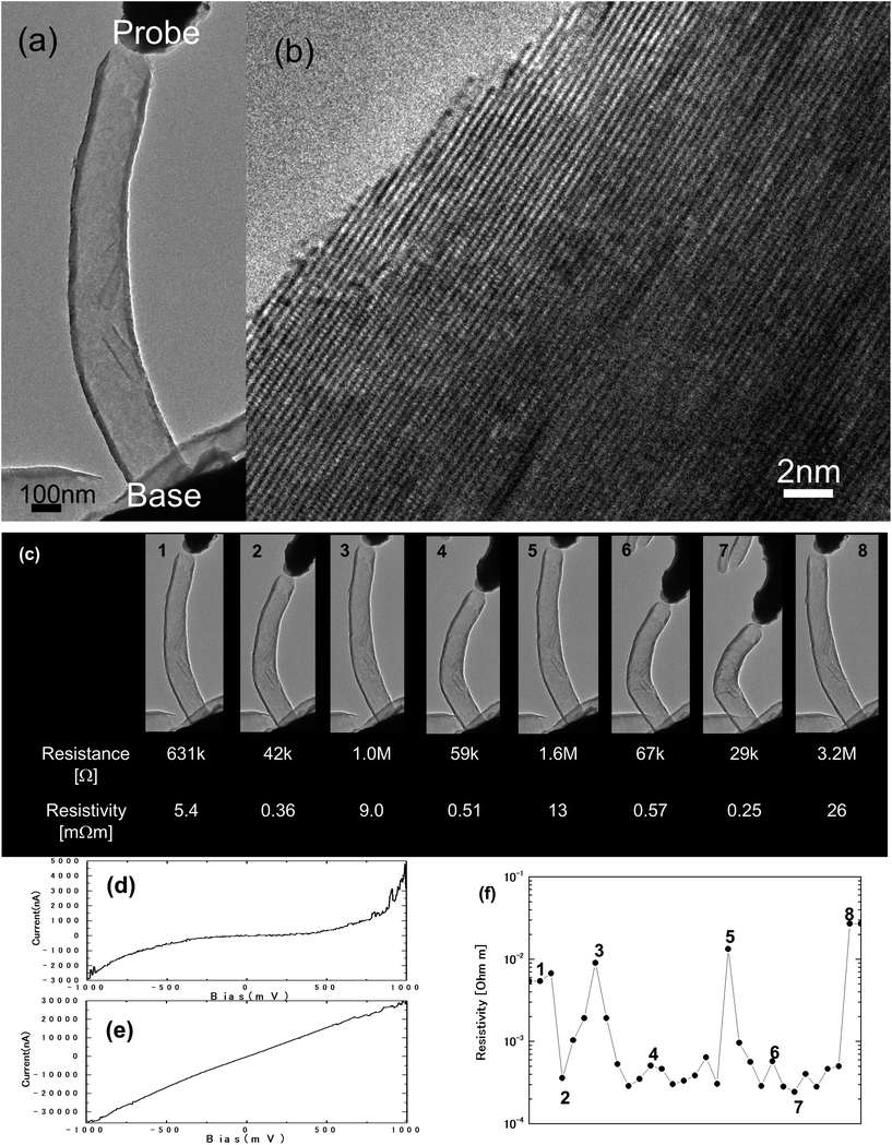 | ||
| Fig. 1 (a) HRTEM image of the CSCNT used for the I–V measurement under compressive load; (b) HRTEM image of the sidewall of the CSCNT which is free of deposited amorphous carbon. (c) Selected TEM images from a CSCNT deformation sequence and their corresponding resistance and resistivity, (d) I–V curve obtained from the CSCNT shown in (c) made contact between the probes without apparent deformation. (e) I–V curve obtained from the same CSCNT deformed under compressive load, and (f) resistivity graph of the whole deformation sequence. Numbers indicate the points where the images are shown in (c). | ||
The observed phenomenon is quite intriguing considering the fact that the CSCNT has a structure in which individual cup-shaped graphene units are stacked to form a tube, and its resistivity can be assumed to be similar to the c-axis resistivity of graphite. The c-axis resistivity, or out-of-plane resistivity, of micrometer-sized highly oriented pyrolytic graphite and natural graphite is reported to be around 10−2 to 10−3 Ω m,14 which is 102 to 104 times greater compared to the graphite in-plane resistivity. In macroscopic natural graphite samples, the c-axis resistivity ranges from 10−4 to 10−5 Ω m, which is imagined to be due to the interlayer defects.15 Inter-shell conductance was measured for MWCNTs, and was found to be ∼1 Ω m, which is much higher than that of bulk graphite.16 Consequently, high graphite interlayer resistance and MWCNT inter-shell resistance should lead to high resistance in uncompressed CSCNTs as well. Therefore, compressive load applied to a CSCNT seems to be playing a key role in the resistance drop observed in the experiments. Measurements of interlayer spacings under compressive force were performed for several CSCNTs. We found an ∼3% decrease in interlayer spacing compared to the initial spacing. This result is corroborated by molecular dynamics simulations discussed below and also in the ESI S3.† Therefore, we hypothesize that interlayer hopping is enhanced due to greater overlap of π orbitals between the layers. However, interlayer hopping may not be sufficient to explain the resistivity drop observed in the present study, since each cup unit in CSCNTs could be considered to be stacked turbostratically, thus the π orbital overlap would be weak. Finally, it should be noted that the alternative explanation that interplanar covalent bonds induced by in-plane defects could lower the c-axis resistance 17 has been ruled out due to the observed reversibility.
Considering the above-mentioned results, we propose that there should have been an edge-to-edge conduction occurring at the compressed sites of a CSCNT, in which the inter-edge distance has decreased. Since the edge part of the cup units is relatively flexible compared to the wall part, inter-edge distances might easily become small leading to an even greater overlap of π orbitals. This effect could create a virtual planar carbon sp2 hybridized network at the sidewall of the CSCNT as shown in Fig. 2(a). Extended Huckel theory semi-empirical calculations for few-layer graphene with different interlayer distance and rotational (or turbostratic) stacking were performed. For ABAB stacking, it was found that for smaller interlayer distances (0.33 nm) there is a more efficient virtual conduction plane, as observed in the experiment, which is caused by a greater overlap of orbitals when compared to the reference model exhibiting interlayer spacings of 0.34 nm. Some orbital overlaps within the layer could also be found, suggesting the possibility that hopping conduction could occur. The AA stacking model shows overlap within the plane indicating higher possibility of hopping conduction, but again, narrower interlayer spacing leads to higher overlap, especially at the zigzag edge region. When each layer is stacked turbostratically (rotational disordered), the overlap of orbitals is enhanced at the zigzag edge-rich location rather than within the plane. Smaller interlayer distances lead to a higher degree of orbital overlap as observed in the previous models. For a graphene sheet, it is well known that zigzag edges tend to have higher electron density, which may lead to intra-edge conduction18 and inter-edge conduction.19
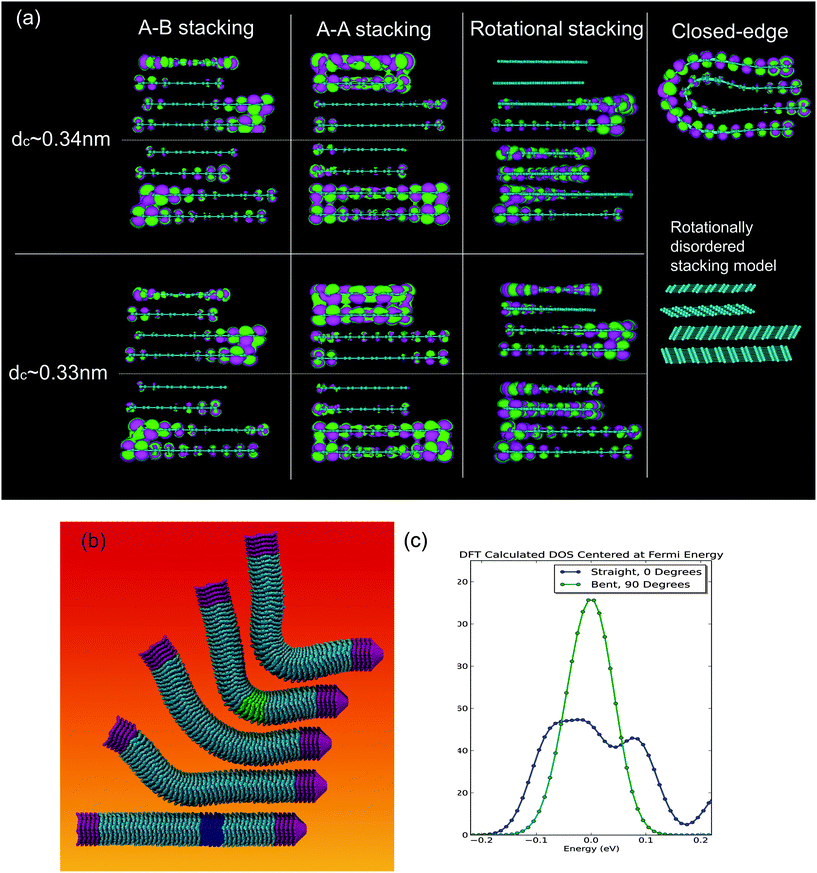 | ||
| Fig. 2 (a) Selected orbital 3D plots for A–B, A–A, and rotationally disordered (turbostratic) stacking graphite models with different interlayer spacing dc. This is a side view of stacked layers, and zig-zag edges are at right and left ends of the models. An orbital plot for the closed-edge model is shown for comparison, and the rotationally disordered stacking model from different viewing angles is shown for the ease of understanding. (b) Snapshots taken from the simulated bending of the CSCNT. The fixed ends of the fiber are highlighted in purple. The straight and bent configurations analyzed with tight binding and DFT are highlighted in blue and green respectively. (c) Electronic density of state curves for the bent and straight configurations highlighted in (b). The calculations show an increase in electron states at the Fermi level when bending occurs. | ||
Molecular dynamics simulations were also performed to replicate the dynamics of the CSCNT bending. The resulting deformed structures were used to calculate the electronic density of states (DOSs) for bent and straight configurations using ab initio density functional theory (DFT) calculations. Simulation methods are detailed in the ESI S3.† Snapshots from CSCNT bending MD simulations are shown in Fig. 2(b), and the fully animated movie is provided as ESI S4.† It is found that when subjected to the stress of bending, an articulated motion of individual cups in the CSCNT allows the tube to bend under substantial stress while avoiding plasticity and topological deformation for angles more than 90 degrees. It is worth noting that this result is in stark contrast to the behavior of other nanofibers such as CNTs in which a kink develops early on at around 30 degrees. We note that a nearest neighbor analysis (see the ESI S3 for details†) to determine wall-to-wall separation for sections on the inner and outer sides of the bend showed that the inner side undergoes a decrease in the average wall-to-wall spacing of 2.80% when bent, which is in good agreement with the experimental result (∼3%). Electronic density of state data obtained by DFT are plotted in Fig. 2(c). The plot is centered at the Fermi energy which has been set to 0 eV. There is a slight increase in the DOS at the Fermi energy. Such an effect, while small, is consistent with an increase in conductivity of the CSCNT when bent and compressed. The increase in DOS at the Fermi energy is related to the increased electronic delocalization along the CSCNT driven by local increases in van der Waals interactions between subsequent cups. This in turn implies an increase in electrical conductivity.
It is worth noting that typically, bent CNTs develop “kink” deformations as well as possible bond hybridization around these kinks. These defects occur at angles well below 90 degrees and have been shown to reduce significantly the conductivity of the CNT,20 in contrast to what we have observed for CSCNTs.
By comparing these results with the calculations of a closed-edge (loop) shown in Fig. 2(a), we should notice that the orbital overlap found in the stacked graphene edge is, in essence, similar to the one found in the looped edge, and therefore suggesting the possibility of edge-to-edge conduction through a virtual conduction plane formed at the edge. This can explain the low resistance that is comparable to MWCNTs, which has a continuous conduction plane along the longitudinal direction. This hypothesis can also be supported by the following experimental results:
By applying excessive current to the same CSCNT that is shown in Fig. 1, the generated Joule heat resulted in a significant increase of temperature and the subsequent formation of loops at the edges of adjacent cups.21 Current–voltage measurements of the annealed CSCNT under compressive stress were also performed (Fig. 3(a)). It was found that when the contact with the electrode is made the I–V profile of the annealed CSCNT was Ohmic, and the resistance (and resistivity) remained more or less stable even under large compressive stress (Fig. 3(b)). It was also found that due to the covalent interconnection of each cup units at the edges, the annealed CSCNT became less flexible. A higher magnification image shows that several neighboring cups are now connected by the loops formed at both outer and inner edges of the cups (Fig. 3(c)), and appear to have formed a continuous conduction path throughout the tube. The resistance and resistivity were close to the lowest value that was measured for compressed CSCNTs, and was also comparable to the resistance of MWCNTs. The full-animated sequence of the deformation and current–voltage measurements of looped CSCNTs is provided in the ESI S5.† When a larger diameter CSCNT, shown in ESI S2,† was annealed, it showed a lower resistance value of 46 Ω (7.2 × 10⁻⁷ Ω m), which was also comparable to that of compressed large diameter CSCNTs. It is natural to consider that the closed-edges (or loops) are good conduction paths that resulted in low resistance when compared to uncompressed CSCNTs.
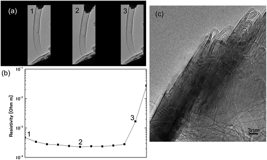 | ||
| Fig. 3 (a) Selected HRTEM images from an annealed CSCNT deformation sequence, (b) resistivity plot of the whole sequence. Numbers (1, 2, and 3) correspond to the image numbers shown in (a), and (c) HRTEM image of the edge of an annealed CSCNT. The edges are closed by the connection of adjacent layers. | ||
Electron energy loss spectroscopy (EELS) measurement of the carbon K-edge of the CSCNT sidewall during the axial compression process revealed that the π* intensity ratio relative to σ* increases as the CSCNT gets compressed (Fig. 4). Considering the structural aspect of the CSCNT, an increase of the graphene edge states results in larger π*/σ* ratios. Moreover, annealed CSCNTs with loop structures showed similar π*/σ* ratios to the compressed CSCNTs, thus confirming that similar edge states appear in both closed-edges (loops) and compressed edges. This result is consistent with the calculations shown in Fig. 2, in which π orbitals might have higher density at the edges, and higher DOS at the Fermi energy.
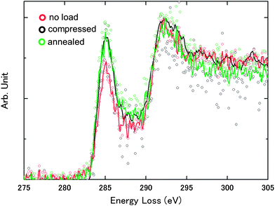 | ||
| Fig. 4 Carbon K-edge EELS obtained from the sidewall of CSCNTs before axial loading (red circle), during compression (black circle), and the annealed CSCNT with loops (green circle). Curve fitted lines with corresponding colors are shown for the ease of understanding, and the spectra are normalized with the s* peak at around 292 eV. | ||
By taking these results into account, it strongly suggests that the graphene edges of the compressed CSCNT formed a virtual conductive plane as described above, thus leading to the significant decrease in resistance reported here. Other authors have reported the synthesis of CSCNTs, exhibiting a continuous helical ribbon-like structure, that were produced under different experimental conditions.22 However, even if this helical ribbon structure was present in our CSCNTs, we believe that upon bending these fibers would exhibit an enhancement in electrical transport, and the modification of the edge–edge conduction channels would still occur in a similar way. Therefore, further measurements should be carried out to explore these helix-spiral conical nanofibers in the near future.
We have performed an in situ current–voltage measurement of CSCNTs deformed under compressive loads, and found that the electronic properties reversibly changed from semiconducting to metallic, and the resistance decreased significantly to a value comparable to that of MWCNTs and graphite. After unloading, the CSCNTs recovered their initial shape and resistivity, returning to the semiconducting type. Joule heating experiments on the same CSCNTs showed that the edges of individual cups coalesced into loops. These annealed CSCNTs also exhibited enhanced transport, similar to the compressed CSCNTs, and highly crystalline MWNTs, suggesting that a similar conduction mechanism has taken place in compressed and annealed CSCNTs. In order to explain this phenomenon, we have suggested a novel edge-to-edge conduction mechanism that forms a virtual conduction plane at the compressed side of the CSCNT. Our findings open up a new possibility of using CSCNTs in the fabrication of strain sensing devices and smart composites that could operate under determined compression. In addition, our findings provide important insight related to the c-axis resistance of graphite, which has been studied since the 1960s. To the best of our knowledge, there is no detailed resistance study reporting the effect of loop formation along the c-axis, although some studies have shown that heat treated samples at >2273 K form loops at the graphene edges.23 Therefore, our results could now explain some of the discrepancies reported in the past related to the c-axis resistance values obtained in different graphitic systems (pristine and thermally annealed).
Experimental methods
CSCNTs were prepared using a synthesis method similar to that reported in ref. 1. They were subsequently oxidized in air at 800 K in order to remove deposited carbon from their surface so that the edges were totally exposed. The resulting oxidized CSCNTs were attached to a gold wire (ϕ 0.3 mm) using conducting tape, and the resultant complex was mounted in a Nanofactory TEM-STM probe holder. In situ measurements were performed in a JEOL JEM-2100F operated at 80 keV. Current–voltage measurements were performed by sweeping the voltage between ±1000 mV with 400 sampling points.Acknowledgements
This work was supported by Grant in Aid from JSPS. MT thanks JST-Japan for funding the Research Center for Exotic Nano Carbons, under the Japanese regional Innovation Strategy Program by the Excellence. VM is supported by the US Army Research Laboratory through the Multiscale Modeling of Electronic Materials Collaborative Research Alliance. B.G.S. was supported by the Center for Nanophase Materials Sciences (CNMS), sponsored at Oak Ridge National Laboratory (ORNL) by the Scientific User Facilities Division, U.S. Department of Energy. Some of the calculations used resources of the Oak Ridge Leadership Computing Facility at the ORNL.References
- M. Endo, Y. A. Kim, T. Hayashi, Y. Fukai, K. Oshida and M. Terrones, et al., Structural characterization of cup-stacked-type nanofibers with an entirely hollow core, Appl. Phys. Lett., 2002, 80, 1267–1269 CrossRef CAS.
- Y. A. Kim, T. Hayashi, Y. Fukai, M. Endo, T. Yanagisawa and M. S. Dresselhaus, Effect of ball milling on morphology of cup stacked carbon nanotubes, Chem. Phys. Lett., 2002, 355279–355284 Search PubMed.
- Q. Liu, W. Ren, Z.-G. Chen, L. Yin, F. Li, H. Cong and H.-M. Cheng, Semiconducting properties of cup-stacked carbon nanotubes, Carbon, 2009, 47, 731–736 CrossRef CAS.
- E. D. Minot, Y. Yaish, V. Sazonova, J.-Y. Park, M. Brink and P. L. McEuen, Tuning Carbon Nanotube Band Gaps with Strain, Phys. Rev. Lett., 2003, 90, 156401 CrossRef CAS.
- T. Kuzumaki and Y. Mitsuda, Dynamic measurement of electrical conductivity of carbon nanotubes during mechanical deformation by nanoprobe manipulation in transmission electron microscopy, Appl. Phys. Lett., 2004, 85, 1250 CrossRef CAS.
- D. Goldberg, P. M. F. J. Costa, M.-S. Wang, X. Wei, D.-M. Tang, Z. Xu, Y. Huang, U. K. Gautam, B. Liu, H. Zeng, N. Kawamoto, C. Zhi, M. Mitome and Y. Bando, Nanomaterial Engineering and Property Studies in a Transmission Electron Microscope, Adv. Mater., 2012, 24, 177–194 CrossRef.
- S. Frank, P. Poncharal, Z. L. Wang and W. A. de Heer, Carbon Nanotube Quantum Resistors, Science, 1998, 280, 1744–1746 CrossRef CAS.
- J. Y. Huang, S. Chen, S. H. Jo, Z. Wang, D. X. Han, G. Chen, M. S. Dresselhaus and Z. F. Ren, Atomic-scale imaging of wall-by-wall breakdown and concurrent transport measurements in multiwall carbon nanotubes, Phys. Rev. Lett., 2005, 94, 236802 CrossRef CAS.
- H. Dai, E. W. Wong and C. M. Lieber, Probing Electrical Transport in Nanomaterials: Conductivity of Individual Carbon Nanotubes, Science, 1996, 272, 523–526 CAS.
- P. G. Collins, M. S. Arnold and P. Avouris, Engineering Carbon Nanotubes and Nanotube Circuits Using Electrical Breakdown, Science, 2001, 292, 706–709 CrossRef CAS.
- H. T. Soh, C. F. Quate, A. F. Morpurgo, C. M. Marcus, J. Kong and H. Dai, Integrated nanotube circuits: Controlled growth and ohmic contacting of single-walled carbon nanotubes, Appl. Phys. Lett., 1999, 75, 627 CrossRef CAS.
- J. Cumings and A. Zettl, Phys. Rev. Lett., 2004, 93, 086801 CrossRef.
- A. Bachtold, M. Henny, C. Terrier, C. Strunk, C. Schonenberger, J. P. Salvetat, J. M. Bonard and L. Forro, Appl. Phys. Lett., 1998, 73, 274 CrossRef CAS.
- L. Casparis, Conductance Anisotropy in Natural and HOPG Graphite, MSc, thesis, Supervisor: D. M. Zumbuhl, University of Basel, 2010.
- K. Matsubara, K. Sugiura and T. Tsuzuku, Phys. Rev. B: Condens. Matter Mater. Phys., 1990, 41, 969 CrossRef CAS; H. Kempa, P. Esquinazi and Y. Kopelevich, Phys. Rev. B: Condens. Matter Mater. Phys., 2002, 65, 241101 CrossRef.
- B. Bourlon, C. Miko, L. Forró, D. C. Glattli and A. Bachtold, Determination of the Intershell Conductance in Multiwalled Carbon Nanotubes, Phys. Rev. Lett., 2004, 93, 17680 CrossRef.
- R. H. Telling, C. P. Ewels, A. A. El-Barbary and M. I. Heggie, Wigner defects bridge the graphite gap, Nat. Mater., 2003, 2, 333 CrossRef CAS.
- K. Wakabayashi, K.-i. Sasaki, T. Nakanishi and T. Enoki, Electronic states of graphene nanoribbons and analytical solutions, Sci. Technol. Adv. Mater., 2010, 11, 054504 CrossRef.
- S. Banerjee, M. Sardar, N. Gayathri, A. K. Tyagi and B. . Raj, Enhanced conductivity in graphene layers and at their edges, Appl. Phys. Lett., 2006, 88, 062111 CrossRef.
- A. A. Farajian, B. I. Yakobson, H. Mizuseki and Y. Kawazoe, Phys. Rev. B: Condens. Matter Mater. Phys., 2003, 67, 205423 CrossRef.
- M. Endo, B. J. Lee, Y. A. Kim, Y. J. Kim, H. Muramatsu, T. Yanagisawa, T. Hayashi, M. Terrones and M. S. Dresselhaus, Transitional behaviour in the transformation from active end planes to stable loops caused by annealing, New J. Phys., 2003, 5, 121 CrossRef.
- J. Vera-Agullo, H. Varela-Rizo, J. A. Conesa, C. Almansa, C. Merino and I. Martin-Gullon, Evidence for growth mechanism and helix-spiral cone structure of stacked-cup carbon nanofibers, Carbon, 2007, 45(14), 2751 CrossRef CAS.
- D. Z. Tsang and M. S. Dresselhaus, The c-axis electrical conductivity of kish graphite, Carbon, 1976, 14, 43 CrossRef CAS.
Footnote |
| † Electronic supplementary information (ESI) available. See DOI: 10.1039/c3nr01887c |
| This journal is © The Royal Society of Chemistry 2013 |