DOI:
10.1039/C8NR01588K
(Paper)
Nanoscale, 2018,
10, 9087-9096
Selectively arranged single-wire based nanosensor array systems for gas monitoring†
Received
24th February 2018
, Accepted 7th April 2018
First published on 1st May 2018
Abstract
Gas nanosensors, comprised of arrays of nanoelectrodes with finger-widths of ∼100 nm developed by electron beam lithography and aerosol assisted chemical vapor deposited non-functionalized and Pt-functionalized tungsten oxide nanowires (<100 nm) subsequently integrated across the pairs of electrodes via the dielectrophoresis method, are developed in this work. The functionality of these devices is validated towards various concentrations of NO2 and C2H5OH. The results demonstrate reproducible and consistent responses with better sensitivity and partial selectivity for the non-functionalized systems to NO2, as opposed to the Pt-functionalized systems, which display better sensing properties towards C2H5OH with a loss of response to NO2. These results are explained on the basis of the additional chemical and electronic interactions at the Pt/tungsten oxide interface, which increase the pre-adsorption of oxygen species and make the functionalized surface rather more sensitive to C2H5OH than to NO2, in contrast to the non-functionalized surface.
Introduction
One-dimensional (1D) metal oxide (MOX) nanostructures in the form of nanowires (NWs), nanotubes, nanorods or nanobelts have demonstrated to play a significant role in the functional properties of different components (e.g., solar cells, supercapacitors, smart windows, photodetectors, biosensors, and gas sensors),1,2 improving typically their performance, as opposed to bulk MOXs. The high aspect ratios of 1D nanostructures, with nanometric widths or diameters (between 1 and 100 nm) and micrometric lengths that allow for their connection with the macroscopic world, make these structures attractive for device miniaturization enabling low power consumption, as demonstrated previously in single-NW-based devices, including gas sensors.4
1D MOX nanostructures are attractive for gas sensors because they have been proven to enhance the functionality of these devices, providing better sensitivity, stability, and to some extent better selectivity not only due to their higher surface area to volume ratio, as opposed to bulk materials, but also due to the presence of specific crystal facets that provide a particular electronic structure to the surface.5,6 Further enhancements on the gas sensing properties of MOXs have also been achieved by the functionalization (or surface modification) of the MOX with second-phase materials (particularly noble metal nanoparticles (NPs) with sizes less than 10 nm),7 providing chemical sensitization via the promotion of gas–solid interactions with spillover of active species from the second-phase material to the MOX surface and/or electronic sensitization of the MOX via the regulation of the charge carrier concentration at the interface of the MOX and the second-phase material.8
Gas sensors based on functionalized 1D MOX nanostructures (e.g., tungsten oxide NWs functionalized with Pt NPs) have been used previously for monitoring various toxic and hazardous gases. In particular, tungsten oxide has attracted much attention due to its sensitivity to nitrogen oxides or ozone,9,10 whereas functionalized structures with dispersed Pt NPs have demonstrated better sensitivity to hydrogen, ethanol and toluene.2,3,11 Tungsten oxide has been synthesized previously in a variety of forms (particles, wires, rods, etc.) using wet- or vapor-chemical routes, and recently we have achieved the formation of tungsten oxide NWs and their functionalization with Pt NPs in a single-step process via a vapor–solid (VS) mechanism enabled by the Aerosol-Assisted Chemical Vapor Deposition (AACVD) of tungsten hexacarbonyl [W(CO)6] and an inorganic platinum precursor (H2PtCl6·xH2O).3
Previous studies demonstrated that gas sensors based on a single (or few) -wire structures connected in parallel are the ideal architecture to achieve a well-defined conduction channel that is easy to modulate by external stimuli (e.g., gaseous molecules) and with better gas detection efficiency compared to bulk materials or multiple wire systems. This improved efficiency, in single-wire systems, is attributed to the lack of grain boundaries and thus more efficient transfer of charge with a lower probability of recombination.5,12,13 Nevertheless, current gas sensor devices based on wires still depend on the wire–wire interfaces, despite the loss of efficiency that this architecture introduces, due to the relatively easier technological steps to integrate multiple-wire based films into devices, as opposed to single-wires.2 Focus ion beam (FIB) has demonstrated to be a useful tool to connect and fabricate single-wire devices, particularly in academic research, however, this technique restricts the scalability of the process and increase the cost and time of fabrication.14,15 In contrast, the dielectrophoresis (DEP) method has become an attractive and robust manufacturing technique for positioning wires across contacts, often in microscale systems with single16 or multiple wires (e.g., in interdigitated electrodes),17 however, its use on nanoscale systems and in particular on arrays for gas sensing (without the need for a contact step with FIB) is still rarely found in the literature.
In this context, recently, we have advanced on the development of nanoelectrode array systems for the integration of single-NWs connected in parallel.18 These systems indicated suitability for the selective integration of single-NWs connected across arrays of electrodes using the dielectrophoresis (DEP) method, and here we describe their fabrication in detail, their functionality and the sensing mechanism of these systems based on non-functionalized or Pt-functionalized tungsten oxide NWs synthesized via AACVD.
Sensor fabrication and characterization methods
The fabrication of the nanosensors involved three processing steps that included (1) development of nanoelectrode arrays, (2) AACVD of non-functionalized or Pt-functionalized tungsten oxide NWs and (3) integration of both systems (i.e., nanoelectrodes and NWs) via the DEP method. These processing steps are described in detail below.
Nanoelectrode arrays
Nanoelectrode arrays with 15, 30, 45 or 60 electrodes connected in parallel were produced at the wafer-level by employing various fabrication steps, including electron-beam lithography (EBL, Raith, E-beam writer Raith150 Two), direct writing laser lithography (DWL, Heidelberg Instruments, DWL 66-fs), metallization (Ion Beam Sputtering, Kaufman & Robinson—KRI®), passivation (RF Magnetron Sputtering, Bestec), ion beam etching (IBE, SCIA system, SCIA coat 200), reactive ion etching (RIE, Oxford Instruments, Plasma NGP 80) and dicing (Oxford Lasers, A-series). Overall, in this work, the resists were used following the standard conditions recommended by Allresist GmbH general product information. Fig. 1 displays a schematic view of the main processing steps carried out for the fabrication of the array of nanoelectrodes. Initially, a SiO2/Si wafer (Fig. 1a) was covered with gold (100 nm thick) (Fig. 1b). Subsequently, the calibration marks were developed by DWL using a positive tone resist (Allresist GmbH, AR-P 3540) (Fig. 1c and d) in order to facilitate the next step, i.e., the EBL process employed to define the nanoelectrodes with finger-widths of 100 nm. Thus EBL was performed at 20 kV using the stitching strategy by 100 μm area on a positive tone electron beam resist (Allresist GmbH, AR-P 6200-13) with 400 nm thickness (Fig. 1e), afterwards IBE was used to etch the gold and pattern the fine electrodes (Fig. 1f). The microelectrodes and contact PADs were achieved by DWL; this process was carried out using a negative-tone optical-active resist (Allresist GmbH, AR-N 4340) with 1.4 μm thickness (Fig. 1g) which also served as a temporary protective mask for the gold layer and the prior formed EBL structures. After development, IBE was repeated to establish the contact between the micro and nanoelectrodes (Fig. 1h). Next, we use a double-stack bilayer of a negative tone optical resist (Allresist GmbH, AR-N 4340 on top) mixed with a non-optical transparent resist layer (Allresist GmbH, AR-BR 5460 on bottom). This bilayer was used to cover the nanoelectrodes and PADs during the RF magnetron sputtering (Bestec, Magnetron sputtering system) of a SiO2 layer (250 μm thick), which was subsequently removed by lift-off (Fig. 1i). Finally, the dicing procedure (5 × 5 mm) was performed using a compact laser micromachining system (Oxford Lasers, A-series), followed by cleaning (Microchem, PG Remover) to remove the residual resist and other organic compounds from the surface.
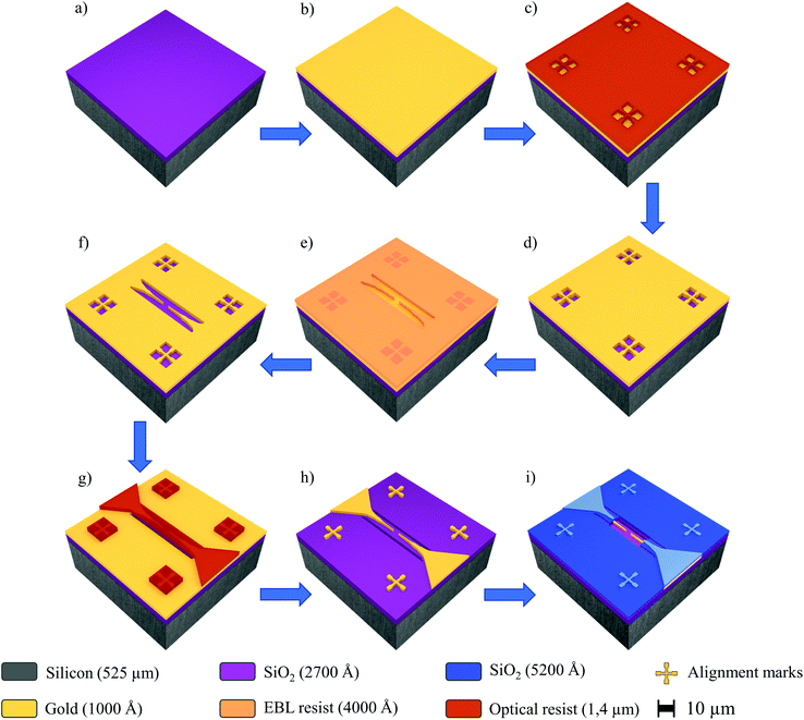 |
| | Fig. 1 Simplified schematic view of the steps used to fabricate the array of nanoelectrodes (not to scale). SiO2/Si wafer (a) sputtered gold on SiO2/Si wafer (b) patterned of alignment marks (10 μm) for stitching fields – alignment procedure (c) gold structures after IBE (d) EBL resist layer for the nanoelectrode patterning (e) gold structures after IBE (f) DWL resist for the microelectrode patterning (g) final gold structure after IBE (h) SiO2 insulation layer patterned (i). | |
Synthesis of functionalized tungsten oxide NWs
Pt-Functionalized tungsten oxide NWs were co-deposited via AACVD from a methanolic solution (5 ml, Penta, ≥99.8%) of W(CO)6 (20 mg, Sigma-Aldrich, ≥97%) and H2PtCl6·xH2O (4 mg, Sigma-Aldrich, 99.9%), whereas non-functionalized tungsten oxide NWs were deposited from a methanolic solution (5 ml, Penta, ≥99.8%) containing only W(CO)6 (20 mg, Sigma-Aldrich, ≥97%). Both processes were carried out on bare silicon tiles (2 × 2 mm) at 390 °C by employing the AACVD system described previously.2 The aerosol droplets of this solution were transported to the heated substrate using a constant nitrogen gas flow (200 sscm) that needed 45 min to transport the entire volume of solution (i.e., 5 ml). Overall, the AACVD of W(CO)6 or W(CO)6 co-reacted with H2PtCl6·xH2O resulting in the formation of relatively weakly adhered (easily abraded or removed by sonication) uniform NW-based films, with diameters and lengths of approximately 100 nm and 10 μm, respectively. The characteristic top view and cross-sectional SEM images of the as-grown films are displayed in Fig. 2. Prior to integrating the NWs into the nanoelectrode array, the NWs were removed from the silicon tiles by sonication (10 s) in water (the suspended NWs in water remained stable for several weeks showing unchanged properties).
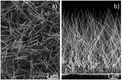 |
| | Fig. 2 Top view and cross-sectional SEM images of the NW based films. Non-functionalized and Pt-functionalized tungsten oxide nanowires showed similar characteristics at microscale. | |
On-chip integration
NWs, suspended in water, were integrated into the nanoelectrode array via the DEP process using an alternating voltage (5Vpp, 9.5 MHz, Agilent 33220A) for 20 s, as illustrated in (Fig. 3). To this end, a contact angle measurement station (SEO, Phoenix 300) provided with two CCD cameras to control the volume of the drop (0.7 μl) and facilitate the alignment of the syringe with the electrode system was also employed. Prior to the integration of NWs, the array of nanoelectrodes was cleaned with oxygen plasma to remove unwanted organic impurities and activate the localized hydrophilic surface patterned around the electrodes. Electrical measurements were also performed to confirm the open circuit between the electrodes before the integration of nanowires.
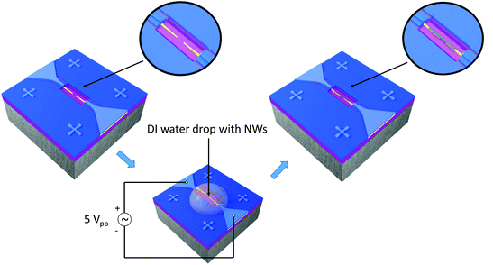 |
| | Fig. 3 On-chip integration steps showing a pair of electrodes connected to the AC voltage source, the droplet with the suspended nanowires for the DEP process and a single-nanowire connected across the electrodes after DEP (not to scale). | |
Additionally, a resistive heating element was also developed to control the temperature of the Si-based chip during the gas sensing tests. This element was attached to the bottom of the nanosensor array system using silver glue (RS Pro, type 186-3593), and then mounted on a TO-8 package interconnected by gold wires (Wire bonder TPT, HB16) to the pins, as shown in Fig. 4. The heating element consists of a multilayer thick film coated on the top of an alumina substrate (99% Al2O3, 250 μm thick).19 The multilayer thick film comprises a conductive layer for electrical connection, ruthenium resistive layer for heating and glass cover layer for electrical insulation.
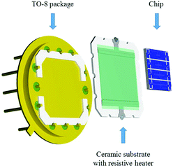 |
| | Fig. 4 Schematic view of the elements comprising the gas-sensing device. | |
Characterization methods
Samples were examined using scanning and transmission electron microscopy (SEM; Tescan FE Mira II LMU and TEM; FEI Tecnai F20, 200 kV) equipped with an Energy Dispersive X-ray detection system (EDX), X-ray diffraction (XRD; Rigaku SmartLab 3 kW, Cu Kα radiation) and X-ray photoelectron spectroscopy (XPS—Phoibos 150 analyzer—SPECS GmbH, Berlin, Germany – under ultrahigh vacuum conditions (base pressure 1 × 10⁻¹⁰ mbar) and a monochromatic Kα X-ray source, 1486.74 eV). Gas sensing tests of the gas sensor devices were carried out towards ethanol (C2H5OH) and nitrogen dioxide (NO2) by monitoring the electrical resistance changes of the NWs while applying different currents in the order of nanoamperes (Keithley 2400 SourceMeter®). The sensors were exposed to various concentrations of C2H5OH or NO2 for five minutes in a continuous flow test chamber (200 sccm) provided with mass-flow controllers, and subsequently, the test chamber was purged with synthetic air for five minutes until the initial baseline resistance was recovered. The sensor response was defined as (ΔR/Rair), i.e., (Rair − Rgas/Rair) for ethanol (reductive gas) and (Rgas − Rair/Rair) for nitrogen dioxide (oxidative gas), where Rair is the sensor resistance in air in the stationary state and Rgas is the sensor resistance after five minutes of analyte exposure.
Results and discussion
Single-wire based nanosensor array systems
The processing steps described above led to the fabrication of gas sensing systems consisting of various parallel-connected pairs of nanoelectrodes with a single-NW interconnected across each pair. Generally, the integration of single-NWs into the nanoelectrode arrays (15 pairs) resulted in a success rate of approximately 33%, thus each nanosensor employed in this work consisted of arrays of 5 single-NWs (non-functionalized or Pt-functionalized). The SEM images of the nanoelectrode array and a single-NW interconnected across a pair of electrodes after the DEP process are displayed in Fig. 5.
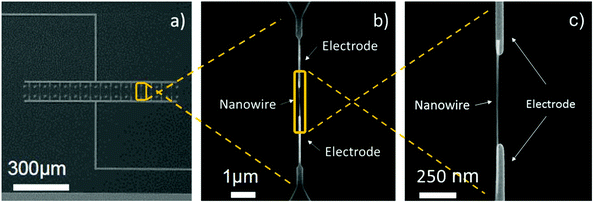 |
| | Fig. 5 View of the nanoelectrodes connected in parallel (a) and detail view of a pair of electrodes with a NW interconnected across them (b)(c). | |
Analysis of the NWs (non-functionalized and Pt-functionalized) using XRD, TEM and XPS indicated the formation of monocrystalline tungsten oxide NWs with a monoclinic phase (P21/n space group, a = 7.306 Å, b = 7.540 Å, c = 7.692 Å, and β = 90.88°; ICCD card no. 72-0677) and preferred orientation in the [010] direction, inferred by the intense diffraction peaks at 23.5° 2θ (d = 3.7 Å) and 48.2° 2θ (d = 1.8 Å), corresponding to the (020) and (040) reflections of the tungsten oxide monoclinic phase, as well as by the marked planar spacing (3.5 ± 0.2 Å) observed by HRTEM (Fig. 6).
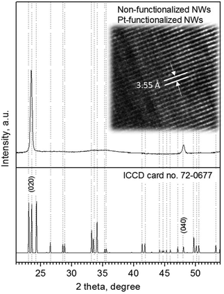 |
| | Fig. 6 Typical XRD pattern and HRTEM (in set image) of the non-functionalized and Pt-functionalized tungsten oxide NWs. Overall XRD patterns indicated a monoclinic phase (P21/n) with the peaks of high intensity (preferred orientation) indexed to the ICCD card no. 72-0677 consistent with previous reports.3 | |
TEM images of the NWs removed from the substrate by sonication and re-deposited on Cu grids confirmed the wire-like morphology with diameters between 50 and 100 nm. Non-functionalized NWs displayed a clean surface (Fig. 7a), whereas Pt-functionalized NWs displayed a surface covered with quasi-spherical nanoparticles of 1 to 5 nm dispersed along the NW surface (Fig. 7b). Localized EDX of these structures confirmed the presence of W on the non-functionalized NWs, and W and Pt on the functionalized NWs. Moreover, analysis of the W 4f core level spectrum recorded on the non-functionalized (inset Fig. 7a) and Pt-functionalized (inset Fig. 7b) tungsten oxide NWs showed similar peak positions to those obtained in a tungsten oxide powder standard, with the peaks broadening in the NW-based films likely due to the presence of higher surface defects at the NWs, as noticed in previous studies.20 The XPS spectrum recorded on the Pt-functionalized NWs (inset Fig. 7b) also demonstrated the presence of Pt 4f core level peaks (found for Pt![[thin space (1/6-em)]](https://www.rsc.org/images/entities/char_2009.gif) :W 3.7%), thus corroborating the incorporation of Pt at the tungsten oxide surface.
:W 3.7%), thus corroborating the incorporation of Pt at the tungsten oxide surface.
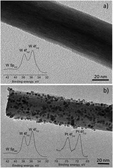 |
| | Fig. 7 TEM of the non-functionalized (a) and Pt-functionalized (b) tungsten oxide NWs. The insets display the W 4f and Pt 4f XPS core-level spectrum for each type of wire. | |
Functional properties
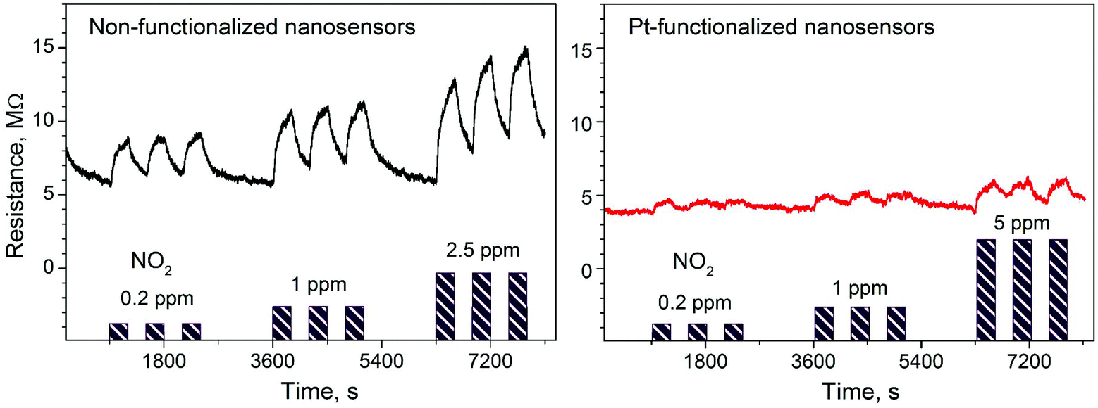
Gas sensing tests of the non-functionalized and Pt-functionalized tungsten oxide nanosensor array systems were carried out at different temperatures (from RT to 250 °C) and currents (from 10 to 100 nA) to find the maximum sensor responses to C2H5OH and NO2 at 250 °C and a better signal-to-noise ratio when using a constant current of 50 nA. Under these conditions, the nanosensors showed consistently an increase or decrease of the electrical resistance after exposure to NO2 (Fig. 8) or C2H5OH (Fig. 9), respectively, as noticed previously for other n-type MOX (including tungsten oxide) when exposed to oxidative or reductive species.10 These electrical resistance changes were proportional to the gas concentration (Fig. 10) and reproducible, displaying similar characteristics (e.g., magnitude of the electrical resistance change and time of response and recovery) for the same gas concentration, as shown in Fig. 8, Fig. 9 and the ESI (Fig. S1–S4†). The recovery of the nanosensor (based on non-functionalized or Pt-functionalized NWs) proved slower towards NO2, as opposed to C2H5OH, particularly at the high NO2 concentration tested (i.e., 2.5 and 5 ppm). This is likely related to the need for higher thermal energy for desorption of NO2 at the surface, however, due to the bonding and packaging characteristics, designed not to exceed a temperature of 300 °C, gas sensing tests of the device at higher temperature were not performed in this work.
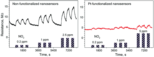 |
| | Fig. 8 Electrical resistance changes of the non-functionalized and Pt-functionalized nanosensors at 250 °C and 50 nA to various concentrations of NO2. Purple color bars represent the concentrations and exposure time to NO2 in each test. | |
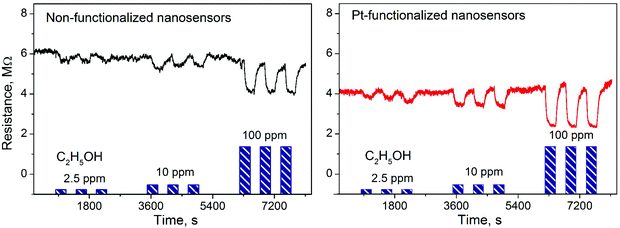 |
| | Fig. 9 Electrical resistance changes of the non-functionalized and Pt-functionalized nanosensors at 250 °C and 50 nA to various concentrations of C2H5OH. Blue color bars represent the concentrations and exposure time to C2H5OH in each test. | |
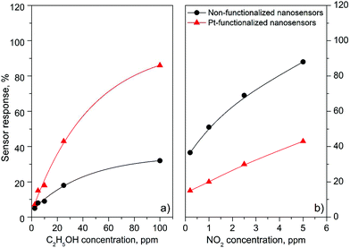 |
| | Fig. 10 Sensor response vs. concentration curves of the non-functionalized and Pt-functionalized nanosensors towards C2H5OH (a) and NO2 (b). | |
Overall, the electrical resistance recorded on the non-functionalized nanosensors showed larger changes towards NO2, as opposed to the Pt-functionalized nanosensors, which showed larger changes towards C2H5OH. For instance the sensor response towards 2.5 ppm NO2 registered a value of approximately 68% for the non-functionalized nanosensors and 30% for those functionalized with Pt NPs, whereas the sensor response towards 100 ppm of C2H5OH registered a value of approximately 32% and 86% for the non-functionalized and Pt-functionalized nanosensors, respectively (Fig. 10). These results indicate a better sensitivity to NO2 for the non-functionalized nanosensors, in contrast to the Pt-functionalized nanosensors, showing consistency with the literature, which previously demonstrated that non-modified tungsten oxide in various forms (e.g., thin films,21 nanoparticles, nanolamellas,22 or nanofibers23) is more sensitive to oxidative species than reductive species,10 even at low concentrations (e.g., 1 ppm (ref. 24)) and in the range of operating temperatures studied in this work. Similarly, these results show better sensitivity to C2H5OH for the Pt-functionalized nanosensors compared to those without functionalization, which is also consistent with previous reports in the literature that demonstrated the enhancement of sensitivity in n-type MOX modified with Pt NPs (e.g., Pt@WO3,25,26 Pt@ZnO,25 or Pt@TiO227) towards reductive species, including C2H5OH.
A comparative table showing the sensor responses recorded in this work and the literature for other single-wire and multiple randomly connected wire systems towards NO2 and C2H5OH is displayed in Table 1. We consider that Table 1 is meant to provide a general idea of the properties of our sensors, despite the complexity behind the comparison of the sensor outputs, which depend strongly on the fabrication and test set-up employed in each work. It is worth noting that Table 1 takes into account only the optimum conditions reported in each work towards NO2 or C2H5OH. Also, that the use of tungsten oxide for single-wire sensors is not frequent in the literature, which has been found to be particularly focused on other MOX wires such as SnO2,28 In2O315,29 or ZnO.30 Based on this literature search, we have noticed that our sensors show better than or similar responses to other single-NW systems reported previously (considering the gas concentrations tested). We also noticed lower magnitudes of response for the single-wire based sensors compared to those based on multiple wires. This is attributed to the broader exposed surface area in multiple wires (as opposed to a single or few NWs), which allows for a greater number of gas molecules to impinge the surface, in turn, amplifying the electrical output signal, as demonstrated previously when comparing the gas sensing performance of thin films and single-NW systems.12
Table 1 Summary of the responses recorded in this work and the literature for sensors based on single and multiple wires towards NO2 and C2H5OH
| Type |
Material |
Features (nm) |
R (%) |
Gas |
ppm |
Ref. |
| S-WA: single-NW array S-W: single-NW M-Ws: multiple wires (wire based films) Ø: wire diameter L: wire length R: response (ΔR/Rair) × 100. |
| S-WA |
WO3 |
100∅ 10000L |
55 |
NO2 |
1 |
This work |
| S-W |
SnO2 |
90∅ 15000L |
25 |
NO2 |
0.5 |
28
|
| S-W |
SnO2 |
78∅ |
100 |
NO2 |
100 |
31
|
| M-Ws |
WO3−x |
50 ∅ |
1560 |
NO2 |
1 |
32
|
| M-Ws |
W18O49 |
90∅ 1000L |
1304 |
NO2 |
1 |
33
|
| M-Ws |
W18O49 |
1000 ∅ |
335 |
NO2 |
1 |
34
|
| M-Ws |
WO3−x |
— |
500 |
NO2 |
5 |
35
|
| S-WA |
Pt@WO3−x |
5 ∅NPs 100 ∅ 10000L |
88 |
C2H5OH |
100 |
This work |
| S-W |
In2O3 |
220∅ 5000L |
47 |
C2H5OH |
100 |
15
|
| S-W |
CP |
220 ∅ 6000 L |
0.15 |
C2H5OH |
2000 |
36
|
| M-Ws |
WO3−x |
100 ∅ 10000 L |
300 |
C2H5OH |
10 |
37
|
| M-Ws |
Pt@WO3−x |
5 ∅NPs 100 ∅ 10000L |
450 |
C2H5OH |
10 |
37
|
| M-Ws |
Au@WO3−x |
30 ∅NPs 200 ∅ 2000L |
98 |
C2H5OH |
4 |
38
|
Further tests of the sensors towards other analytes including carbon monoxide (CO) and ammonia (NH3) showed typical n-type semiconducting behaviour during gas exposure (Fig. S1 and S5†). Overall, the responses to CO were negligible, whereas the response to NH3 registered higher values for the non-functionalized nanosensors than for the Pt-functionalized nanosensors. A global view of the results (Fig. S6†) suggests good selectivity for the non-functionalized nanosensors to NO2 with respect to C2H5OH, NH3 and CO, and a moderate cross-response among the reductive gases (i.e., C2H5OH, NH3 and CO). In contrast, Pt-functionalized nanosensors suggest better selectivity among reductive gases compared to the non-functionalized nanosensors, although with a higher probability of interference from NO2 (oxidative gas) to C2H5OH.
Pt-Functionalized nanosensors also displayed sensitivity to humidity (Fig. S7†). However, and despite this property is undesired in gas sensors, strong humidity interference has also been noted in previous reports on tungsten oxide and its modification with Pt,2,39 in agreement with our results.
Gas sensing mechanism
The sensing results can be understood on the basis of the mechanism of chemical sensing on MOX surfaces, in which the pre-adsorbed oxygen species at the MOX react with gaseous analytes producing electrical changes in the MOX. Thus, when non-functionalized NWs are exposed to air, they adsorb oxygen molecules at their surface leading to the formation of different chemisorbed oxygen species (O2− at temperatures lower than 130 °C, O− at temperatures between 130 and 300 °C and O2− at temperatures higher than 300 °C)40 by capturing electrons from the conduction band (eqn (1)–(3)), which in turn produces a depletion layer and an increase in the resistance of the tungsten oxide NWs, as illustrated in Fig. 11a and b. This mechanism is similar to that of the Pt-functionalized NWs (Fig. 11c), although, due to the large difference in the work function of Pt (5.12–5.93 eV)41 and band gap of tungsten oxide (2.5–3.5 eV),42 nano-Schottky barriers are formed at the interface of the Pt NPs and the tungsten oxide NW. This induces an accumulation of electrons on the Pt NPs and the formation of holes on the tungsten oxide NWs,27 thus resulting in an enlargement of the tungsten oxide depletion layer at the surroundings of the Pt NPs. Simultaneously, the catalytic Pt NPs also activate the dissociation of molecular oxygen and their distribution onto the surface of the NW. This effect, known as “spillover”, strongly increases the quantity of adsorbed oxygen species on the tungsten oxide surface (Fig. 11d).
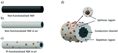 |
| | Fig. 11 A schematic illustration of the sensing mechanism of the non-functionalized and Pt-functionalized nanosensor. Fully conducting tungsten oxide NW (a). Formation of the depletion region around the NW when exposed to air (b) and increase of the depletion region on modification with Pt nanoparticles (c). Formation of Schottky barriers at the Pt NPs and tungsten oxide NW interface contributing to the spillover effect and the enlargement of the depletion region in air (d). | |
After the exposure of the sensors to ethanol at 250 °C the following reaction paths are likely to occur at the surface dominated by pre-adsorbed O−:43,44
| | | C2H5OH(gas) → C2H5O−(ads) + H+(ads) | (4) |
| | | 2H+(ads) + O−(ads) → H2O(vapor) | (5) |
| | | C2H5O−(ads) + H+(ads) → C2H4(vapor) + H2O(vapor) | (6) |
| | | C2H4(vapor) + 6O−(ads) → 2CO2(gas) + 2H2O(vapor) + 6e− | (7) |
| | | C2H5OH(gas) + O−(ads) → C2H4O(ads) + H2O(vapor) + e− | (8) |
| | | C2H4O(ads) + O−(lattice) → CH3COOH(vapor) + Vo | (9) |
Generally C2H5OH molecules are adsorbed on the surface of tungsten oxide via the oxygen atoms of the hydroxyl groups (eqn (4)) and the resultant H+ ions react with O− ions (eqn (5)) to form water molecules which are then desorbed. At elevated temperatures (>200 °C) the adsorbed ethoxy groups can also be decomposed into ethylene and water that later are desorbed from the surface (eqn (6) and (7)). C2H5OH can also be decomposed to acetaldehyde by reaction with the lattice oxygen with subsequent desorption of vapor of acetic acid and the release of electrons towards tungsten oxide due to the formation of oxygen vacancies (VO) (eqn (8) and (9)).43 To sum up, the C2H5OH molecules adsorb at the non-functionalized tungsten oxide surface providing electrons to reduce the adsorbed ionic oxygen and release the free electrons back to the tungsten oxide conduction band. This process reduces the width of the depletion region and increases the conduction of the tungsten oxide NWs.
A similar mechanism occurs for Pt-functionalized tungsten oxide during C2H5OH sensing however with significant improvements in the response to C2H5OH first due to the increment of pre-adsorbed oxygen as a result of the trap and accumulation of oxygen species at the Pt NPs and/or spill of these species over the NW surface and second due to the promotion and acceleration of the reactions described above at the Pt NPs unlike the mechanism occurring at the non-functionalized tungsten oxide surface.45 Hence in contrast to the non-functionalized NWs the Pt-functionalized surface (that is covered with a higher amount of pre-adsorbed oxygen species) promotes the release of more electrons into the tungsten oxide conduction band during C2H5OH adsorption and in turn records larger resistance changes in the Pt-functionalized nanosensors towards C2H5OH.
On the other hand when the NWs are exposed to NO2 the NO2 molecules are adsorbed as NO2− (eqn (10)) capturing electrons from the tungsten oxide conduction band and reacting further with the adsorbed ionic oxygen (eqn (11)) to form nitric oxide and O2−.46
| | | NO2(gas) + e− → NO−2(ads) | (10) |
| | | NO−2(ads) + O−(ads) + 2e− → NO(gas) + 2O2−(ads) | (11) |
These reactions take electrons from the conduction band of the tungsten oxide NW producing a wider depletion layer than that formed during the pre-adsorption of oxygen which results in a further increase of the resistance along the non-functionalized wire. In the Pt-functionalized NWs, as these structures are more depleted of electrons after the pre-adsorption of oxygen, the NO2 molecules exposed to this surface find less electrons in the tungsten oxide conduction band to be accepted and to form NO2− adsorbents, making the Pt-functionalized NW less sensitive to NO2 than to C2H5OH as noticed in the functional tests of these systems.
In summary these results demonstrate a reliable operation of the nanosensors with consistent functional properties that validate the fabrication of the sensing device. The fabrication method reported here which includes the selective integration of functional single-NWs (<100 nm) into an array of EBL developed electrodes with nanoscale finger-widths of ∼100 nm is an attractive route for developing the next generation of single-wire based nanosensors without using non-scalable and time-consuming techniques such as FIB and circumventing the electrical percolation issues of conventional chemoresistive sensors based on sensitive films with multiple NWs.
Conclusions
Single-NW gas nanosensor array systems based on non-functionalized or Pt-functionalized tungsten oxide were fabricated using various processing steps that include electron beam lithography to define the parallel-connected nanoelectrodes, AACVD to grow the NWs and DEP to align single-NWs across each pair of nanoelectrodes. The results demonstrated the selective integration of single-NWs into the array of nanoelectrodes and the gas sensing tests of these systems validated the functionality of the device. Overall the sensor performance proved a reproducible behavior with the Pt-functionalized NWs showing a better response to C2H5OH compared to the non-functionalized NW systems which responded better to NO2; in agreement with similar systems reported previously in the literature. These results were attributed to the additional chemical and electronic interactions at the interface of the Pt NPs and tungsten oxide NWs which increase the pre-adsorption of oxygen species at the functionalized NW surface and in turn the sensitivity to C2H5OH rather than NO2; as opposed to the non-functionalized tungsten oxide surface.
Conflicts of interest
There are no conflicts to declare.
Acknowledgements
This work has been supported by the Czech Science Foundation (GAČR) via Grant No. 17-16531S and in part by the Czech Ministry of Education Youth and Sports of Czech Republic under grant LO141 and CEITEC Nano Research (ID LM2015041 MEYS CR 2016–2019). This research made used of the SIX Research Centre. The support from the Spanish Ministry of Economy and Competitiveness via projects TEC2016-79898-C6 (AEI/FEDER EU) and TEC2015-74329-JIN-(AEI/FEDER EU) is also acknowledged.
Notes and references
- M. Anish Kumar, S. Jung and T. Ji, Sensors, 2011, 11, 5087–5111 CrossRef CAS PubMed; K.-Y. Choi, J.-S. Park, K.-B. Park, H. J. Kim, H.-D. Park and S.-D. Kim, Sens. Actuators, B, 2010, 150, 65–72 CrossRef; L. Chih-Hao, H. Min Hsiung, K. Chi-Yun and L. Ing-Chi, Jpn. J. Appl. Phys., 2014, 53, 06JG08 CrossRef; D. K. Roh, R. Patel, S. H. Ahn, D. J. Kim and J. H. Kim, Nanoscale, 2011, 3, 4162–4169 RSC; K. Joondong, Y. Ju-Hyung, K. Chang Hyun, P. Yun Chang, W. Ju Yeon, P. Jeunghee, L. Jung-Ho, Y. Junsin and H. Chang-Soo, Nanotechnology, 2010, 21, 115205 CrossRef PubMed.
- S. Vallejos, I. Grácia, O. Chmela, E. Figueras, J. Hubálek and C. Cané, Sens. Actuators, B, 2016, 235, 525–534 CrossRef CAS.
- S. Vallejos, I. Gràcia, E. Figueras and C. Cané, ACS Appl. Mater. Interfaces, 2015, 7, 18638–18649 CAS.
- H. Huang, B. Liang, Z. Liu, X. Wang, D. Chen and G. Shen, J. Mater. Chem., 2012, 22, 13428–13445 RSC.
- D. R. Miller, S. A. Akbar and P. A. Morris, Sens. Actuators, B, 2014, 204, 250–272 CrossRef CAS.
- A. Gurlo, Nanoscale, 2011, 3, 154–165 RSC.
- J. F. Mcaleer, P. T. Moseley, J. O. W. Norris, D. E. Williams and B. C. Tofield, J. Chem. Soc. Faraday Trans. 1, 1988, 84, 441–457 RSC.
- A. Kolmakov, D. O. Klenov, Y. Lilach, S. Stemmer and M. Moskovits, Nano Lett., 2005, 5, 667–673 CrossRef CAS PubMed.
- H. G. Moon, S. D. Han, M.-G. Kang, W.-S. Jung, B. Kwon, C. Kim, T. Lee, S. Lee, S.-H. Baek, J.-S. Kim, H.-H. Park and C.-Y. Kang, Sens. Actuators, B, 2016, 229, 92–99 CrossRef CAS; Y. Qin, X. Zhang, Y. Wang and Y. Liu, Sens. Actuators, B, 2017, 240, 477–486 CrossRef.
- S. Vallejos, V. Khatko, J. Calderer, I. Gracia, C. Cané, E. Llobet and X. Correig, Sens. Actuators, B, 2008, 132, 209–215 CrossRef CAS.
- J. Zhang, X. H. Liu, M. J. Xu, X. Z. Guo, S. H. Wu, S. M. Zhang and S. R. Wang, Sens. Actuators, B, 2010, 147, 185–190 CrossRef CAS; I. Lee, S.-J. Choi, K.-M. Park, S. S. Lee, S. Choi, I.-D. Kim and C. O. Park, Sens. Actuators, B, 2014, 197, 300–307 CrossRef.
- E. Brunet, T. Maier, G. C. Mutinati, S. Steinhauer, A. Köck, C. Gspan and W. Grogger, Sens. Actuators, B, 2012, 165, 110–118 CrossRef CAS.
- X. Chen, C. K. Y. Wong, C. A. Yuan and G. Zhang, Sens. Actuators, B, 2013, 177, 178–195 CrossRef CAS; R. M. Penner, Annu. Rev. Anal. Chem., 2012, 5, 461–485 CrossRef PubMed; N. S. Ramgir, Y. Yang and M. Zacharias, Small, 2010, 6, 1705–1722 CrossRef PubMed.
- F. Hernandez-Ramirez, A. Tarancon, O. Casals, J. Rodriguez, A. Romano-Rodriguez, J. R. Morante, S. Barth, S. Mathur, T. Y. Choi, D. Poulikakos, V. Callegari and P. M. Nellen, Nanotechnology, 2006, 17, 5577–5583 CrossRef CAS PubMed.
- G. Domènech-Gil, S. Barth, J. Samà, P. Pellegrino, I. Gràcia, C. Cané and A. Romano-Rodriguez, Sens. Actuators, B, 2017, 238, 447–454 CrossRef.
- E. M. Freer, O. Grachev, X. Duan, S. Martin and D. P. Stumbo, Nat. Nanotechnol., 2010, 5, 525 CrossRef CAS PubMed; S. Junya, N. Nobutaka, H. Shin-ichiro, U. Makoto, I. Kiminobu, H. Mitsuhiro, O. Tatsuo and H. Masanori, Nanotechnology, 2006, 17, 2567 CrossRef PubMed.
- J. Guilera, C. Fàbrega, O. Casals, F. Hernández-Ramírez, S. Wang, S. Mathur, F. Udrea, A. De Luca, S. Z. Ali, A. Romano-Rodríguez, J. D. Prades and J. R. Morante, Sens. Actuators, B, 2015, 221, 104–112 CrossRef CAS.
-
O. Chmela, J. Sadílek, J. Samà, A. Romano-Rodriguez, J. Hubálek and S. Vallejos, in, Proceedings of SPIE - The International Society for Optical Engineering, 102480F.
-
G. Radosavljevic and W. Smetana, in Printed Films, Woodhead Publishing, 2012, pp. 429–468 Search PubMed.
- C. Navío, S. Vallejos, T. Stoycheva, E. Llobet, X. Correig, R. Snyders, C. Blackman, P. Umek, X. Ke, G. Van Tendeloo and C. Bittencourt, Mater. Chem. Phys., 2012, 134, 809–813 CrossRef.
- A. Maity and S. B. Majumder, Sens. Actuators, B, 2015, 206, 423–429 CrossRef CAS.
- T. Liu, J. Liu, Q. Hao, Q. Liu, X. Jing, H. Zhang, G. Huang and J. Wang, CrystEngComm, 2016, 18, 8411–8418 RSC.
- L. Giancaterini, S. M. Emamjomeh, A. De Marcellis, E. Palange, A. Resmini, U. Anselmi-Tamburini and C. Cantalini, Sens. Actuators, B, 2016, 229, 387–395 CrossRef CAS.
- A. J. T. Naik, M. E. A. Warwick, S. J. A. Moniz, C. S. Blackman, I. P. Parkin and R. Binions, J. Mater. Chem. A, 2013, 1, 1827–1833 CAS.
- Y. A. Zhang, J. Q. Xu, P. C. Xu, Y. H. Zhu, X. D. Chen and W. J. Yu, Nanotechnology, 2010, 21 Search PubMed , 285501.
- J. Y. Luo, X. X. Chen, W. Da Li, W. Y. Deng, W. Li, H. Y. Wu, L. F. Zhu and Q. G. Zeng, Appl. Phys. Lett., 2013, 102, 113104 CrossRef; R. J. Bose, N. Illyaskutty, K. S. Tan, R. S. Rawat, M. V. Matham, H. Kohler and V. P. M. Pillai, Europhys. Lett., 2016, 114 Search PubMed , 66002.
- H. Chen, S. Chen, X. Quan, H. T. Yu, H. M. Zhao and Y. B. Zhang, J. Phys. Chem. C, 2008, 112, 9285–9290 CAS.
- J. D. Prades, R. Jimenez-Diaz, F. Hernandez-Ramirez, S. Barth, A. Cirera, A. Romano-Rodriguez, S. Mathur and J. R. Morante, Appl. Phys. Lett., 2008, 93, 123110 CrossRef; J. D. Prades, R. Jimenez-Diaz, F. Hernandez-Ramirez, J. Pan, A. Romano-Rodriguez, S. Mathur and J. R. Morante, Appl. Phys. Lett., 2009, 95, 053101 CrossRef.
- X. Zou, J. Wang, X. Liu, C. Wang, Y. Jiang, Y. Wang, X. Xiao, J. C. Ho, J. Li, C. Jiang, Y. Fang, W. Liu and L. Liao, Nano Lett., 2013, 13, 3287–3292 CrossRef CAS PubMed.
- M. Cardoza-Contreras, J. Romo-Herrera, L. Ríos, R. García-Gutiérrez, T. Zepeda and O. Contreras, Sensors, 2015, 15, 29816 CrossRef PubMed.
- M. Tonezzer and N. V. Hieu, Sens. Actuators, B, 2012, 163, 146–152 CrossRef CAS.
- T. Stoycheva, F. E. Annanouch, I. Gràcia, E. Llobet, C. Blackman, X. Correig and S. Vallejos, Sens. Actuators, B, 2014, 198, 210–218 CrossRef CAS.
- Y. Qin, M. Hu and J. Zhang, Sens. Actuators, B, 2010, 150, 339–345 CrossRef CAS.
- N. Van Hieu, H. Van Vuong, N. Van Duy and N. D. Hoa, Sens. Actuators, B, 2012, 171–172, 760–768 CrossRef CAS.
- A. Ponzoni, E. Comini, G. Sberveglieri, J. Zhou, S. Z. Deng, N. S. Xu, Y. Ding and Z. L. Wang, Appl. Phys. Lett., 2006, 88, 203101 CrossRef.
- D. Yaping, C. Yanyan, E. M. Tom, E. Stephane and A. T. C. Johnson, Nanotechnology, 2009, 20, 434014 CrossRef PubMed.
- S. Vallejos, P. Umek, T. Stoycheva, F. Annanouch, E. Llobet, X. Correig, P. De Marco, C. Bittencourt and C. Blackman, Adv. Funct. Mater., 2013, 23, 1313–1322 CrossRef CAS.
- F. Di Maggio, M. Ling, A. Tsang, J. Covington, J. Saffell and C. Blackman, J. Sens. Sens. Syst., 2014, 3, 325–330 CrossRef.
- C. Zhang, A.-F. Kanta, H. Yin, A. Boudiba, J. D'Haen, M.-G. Olivier and M. Debliquy, Int. J. Hydrogen Energy, 2013, 38, 2929–2935 CrossRef CAS; W.-T. Koo, S.-J. Choi, N.-H. Kim, J.-S. Jang and I.-D. Kim, Sens. Actuators, B, 2016, 223, 301–310 CrossRef.
- S. Lenaerts, J. Roggen and G. Maes, Spectrochim. Acta Part A, 1995, 51, 883–894 CrossRef CAS; M. Sinha, R. Mahapatra, B. Mondal, T. Maruyama and R. Ghosh, J. Phys. Chem. C, 2016, 120, 3019–3025 Search PubMed; J. C. Belmonte, J. Manzano, J. Arbiol, A. Cirera, J. Puigcorbe, A. Vila, N. Sabate, I. Gracia, C. Cane and J. R. Morante, Sens. Actuators, B, 2006, 114, 881–892 CrossRef; N. Barsan and U. Weimar, J. Electroceram., 2001, 7, 143–167 CrossRef.
- M. H. Luo, W. F. Yao, C. P. Huang, Q. Wu and Q. J. Xu, J. Mater. Chem. A, 2015, 3, 13884–13891 CAS.
- Y. Baek and K. Yong, J. Phys. Chem. C, 2007, 111, 1213–1218 CAS.
- D. L. Chen, X. X. Hou, H. J. Wen, Y. Wang, H. L. Wang, X. J. Li, R. Zhang, H. X. Lu, H. L. Xu, S. K. Guan, J. Sun and L. Gao, Nanotechnology, 2010, 21 Search PubMed , 035501.
- K. Mirabbaszadeh and M. Mehrabian, Phys. Scr., 2012, 85, 035701 CrossRef CAS; F. Hellegouarc'h, F. Arefi-Khonsari, R. Planade and J. Amouroux, Sens Actuator B, 2001, 73, 27–34 CrossRef; A. Labidi, E. Gillet, R. Delamare, M. Maaref and K. Aguir, Sens. Actuator B, 2006, 120, 338–345 CrossRef.
- L. M. Petkovic, S. N. Rashkeev and D. M. Ginosar, Catal. Today, 2009, 147, 107–114 CrossRef CAS.
- E. Oh, H. Y. Choi, S. H. Jung, S. Cho, J. C. Kim, K. H. Lee, S. W. Kang, J. Kim, J. Y. Yun and S. H. Jeong, Sens. Actuators, B, 2009, 141, 239–243 CrossRef CAS.
Footnote |
| † Electronic supplementary information (ESI) available. See DOI: 10.1039/c8nr01588k |
|
| This journal is © The Royal Society of Chemistry 2018 |

 Open Access Article
 This Open Access Article is licensed under a Creative Commons Attribution-Non Commercial 3.0 Unported Licence
 ab,
J.
Sadílek
a,
G.
Domènech-Gil
ab,
J.
Sadílek
a,
G.
Domènech-Gil