
 Open Access Article
 This Open Access Article is licensed under a Creative Commons Attribution-Non Commercial 3.0 Unported Licence
Tetradic phosphor white light with variable CCT and superlative CRI through organolead halide perovskite nanocrystals
Gopi C.
Adhikari
 ,
Preston A.
Vargas
,
Hongyang
Zhu
,
Alexei
Grigoriev
and
Peifen
Zhu
*
,
Preston A.
Vargas
,
Hongyang
Zhu
,
Alexei
Grigoriev
and
Peifen
Zhu
*
Department of Physics and Engineering Physics, The University of Tulsa, Tulsa, Oklahoma 74104, USA Web: peifen-zhu@utulsa.edu
First published on 1st March 2019
Abstract
In this work, the emission spectral range of halide perovskite nanocrystals is extended from violet to infrared, the widest emission range for halide perovskites to date. This range extension was made possible by a cost-effective solution-based synthesis process that only involves two halides [MAPb(BrxI1−x)3 and MA = CH3NH3]. Furthermore, the correlated-color temperature (CCT) of white light is tuned by blending an appropriate fraction of the as-synthesized blue, green, yellow, and red emitting nanocrystals. This represents one of the first applications of a tetradic phosphor system for maximizing the color rendering index (CRI) for this material. The CCT ranges from warm to cool white (2759–6398 K) and the CRI has a maximum value of 93.95. Thus, this fourfold phosphor approach demonstrates that halide perovskites are promising alternatives to conventional phosphors in the search for low-cost and high-quality white light sources in the next generation of white lighting technology.
Introduction
Solid-state lighting exhibits a significant reduction in power consumption compared to traditional lighting technologies.1–4 In particular, III-nitride white light-emitting diodes (LEDs) have become increasingly popular due to their high energy efficiency, low energy consumption, and environmental friendliness. These commercialized white LEDs are typically fabricated by placing yellow phosphors (YAG:Ce3+) on commonly available III-nitride blue LEDs.5 The photon down-conversion process that occurs when the LED is turned on yields a mixture of blue and yellow light that observers perceive to be white. The lack of red wavelength components in this approach, however, leaves the produced light with an undesirably cold hue [high correlated color temperature (CCT)] and low color rendering index (CRI).6 In addition, the photon down-conversion phosphors, in this case, give rise to their optical properties from rare-earth metal doping.3,7–10 As can be expected of a substance with “rare” in its name, this substantially drives up the cost of current white LED technology.1,6,11 Therefore, it is imperative to search for higher-quality and lower-cost photon down-conversion materials.Lead halide perovskites and their mixed-halide composites are emerging as a new generation of economic and scalable materials12–16 due to their favourable optoelectronic properties such as strong absorption coefficients,17,18 broadband excitation,19,20 narrow band emission,21,22 broad color gamut,23,24 high quantum yield,25–28 and tunable bandgap.29–33 These properties attest to their future applicability in solid-state devices and may lead to rapid improvement in the performance of optoelectronic devices such as LEDs,34–38 solar cells,39–42 photodetectors,43,44 and lasers.45,46 Many publications have reported the fabrication of white light LEDs using halide perovskites. Some used perovskites as one of the visible color emitting materials combined with a UV/blue LED chip and conventional phosphors.23,47,48 Others have replaced conventional phosphors altogether, using only perovskites with various emission spectra [red, green, and blue (RGB)].49–51 Recently, there has also been success in transforming halide perovskites into single-component white-light emitters.52–54 Thus, there is great potential for nanocrystal integration with III-nitride UV/blue LEDs to achieve high-quality white light and colorful LEDs via the direct combination of materials with different emission spectra.
Here, we demonstrate a breakthrough in photon down-conversion based white LED technology via halide perovskite phosphors. Methylammonium lead mixed-halide MAPb(BrxI1−x)3 perovskite nanocrystals have been synthesized via a solution-based synthesis with stringent ligand-mediation and anion ratio control, resulting in a wide range of narrow line-width emission spectra. The photoluminescence (PL) emission ranges from 408 nm to 755 nm and the band gap extends from 3.04 eV to 1.51 eV. Furthermore, we have estimated white light emission using the perovskite nanocrystals with four-band emission (blue, green, yellow, and red) instead of the usual three-band emission.26,49 By optimizing the contribution of each of the four components, we obtained tunable CCT ranging from 2759 to 6398 K and the CRI reached an unprecedented value of 93.95.
Experimental section
Materials and methods
The synthesis of MAPbBr3 began by adding 0.025 g of MABr and 0.05 g of PbBr2 to a mixture of 0.5 mL of dimethylformamide, 8.5 of mL gamma-butyrolactone, and 15 μL of octylamine (consider, 15 μL of the ligand octylamine as ‘L’). This mixture was stirred at 70–80 °C on a hot plate until the solids dissolved completely and the solution became transparent. Then, this precursor solution was slowly mixed with 5 mL of toluene under magnetic stirring at room temperature. The solution was then centrifuged at 5000 rpm for 5 min to separate the aggregate particles. The supernatant was poured into a clean vial and centrifuged again at 16![[thin space (1/6-em)]](https://www.rsc.org/images/entities/char_2009.gif) 000 rpm for 15 min. The precipitate was then collected by discarding the supernatant. The MAPbI3 precursor solution was prepared using the same procedure as the MAPbBr3 precursor, using 0.036 g of MAI and 0.069 g of PbI2 to replace the bromine components. The MAPbI3 precursor was blended with the MAPbBr3 precursor in the ratio required to achieve the intended composition of MAPb(BrxI1−x)3. In order to shift the PL emission from green to violet, the ligand (octylamine) concentration was increased in the MAPbBr3 precursor only. After synthesis, the nanocrystals were dispersed in toluene for storage and further characterization. This synthesis was performed in an ambient atmosphere.
000 rpm for 15 min. The precipitate was then collected by discarding the supernatant. The MAPbI3 precursor solution was prepared using the same procedure as the MAPbBr3 precursor, using 0.036 g of MAI and 0.069 g of PbI2 to replace the bromine components. The MAPbI3 precursor was blended with the MAPbBr3 precursor in the ratio required to achieve the intended composition of MAPb(BrxI1−x)3. In order to shift the PL emission from green to violet, the ligand (octylamine) concentration was increased in the MAPbBr3 precursor only. After synthesis, the nanocrystals were dispersed in toluene for storage and further characterization. This synthesis was performed in an ambient atmosphere.
Characterization
X-ray diffraction (XRD) measurements were taken using a Rigaku Smart Lab system with a Cu Kα1 (λ = 1.54 Å) fixed anode X-ray source operating at 40 kV and 44 mA. Nanocrystal samples were placed on a glass substrate and dried in an ambient environment before XRD characterization. Transmission electron microscopy (TEM) measurements were performed using a Hitachi H-7000 TEM at 75 kV. Nanocrystal samples for TEM measurements were prepared by diluting them in toluene and sonicating to separate the individual particles. The sample was then carefully placed onto a copper grid with a carbon film and dried in an ambient atmosphere before characterization. The UV-visible absorption spectra were measured using a VARIAN Carry 50 Scan UV-Spectrophotometer with nanocrystals in a toluene colloidal suspension. The PL spectra were measured using a Spectrofluorophotometer (Shimadzu, RF-6000) with a monochromatic xenon lamp as the excitation source while the nanocrystals remained in a colloidal suspension. The LED spectra were obtained by combining four different emissions with different ratios. The calculation of CRI and CCT were performed according to equations defined by the CIE (Commission Internationale de l'Eclairage). Four different emission spectra (blue, green, yellow, and red) were combined and the spectral data were analysed to yield the CRI, CCT, and CIE coordinates.Results and discussion
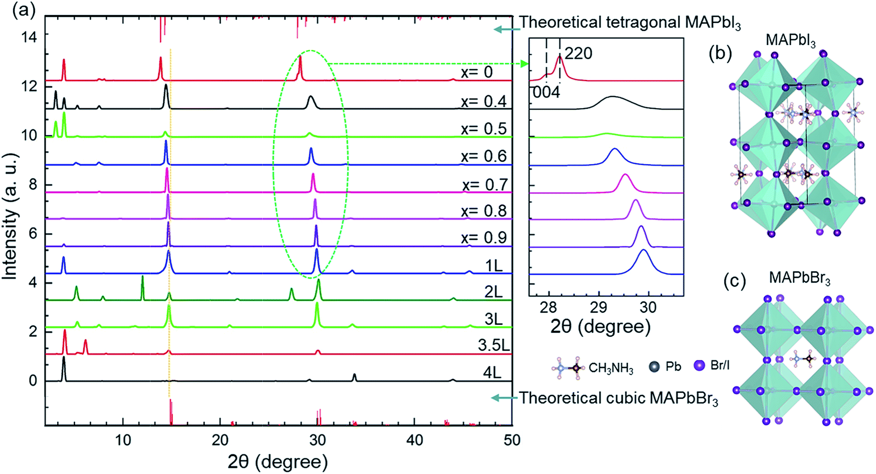
The effects of ligand concentration and compositions of anions on the crystal structure were studied using XRD patterns (Fig. 1a). The sharp diffraction peaks confirm the high crystallinity of the nanocrystals. For MAPbBr3, the diffraction patterns are consistent with the cubic crystal structure with a Pm![[3 with combining macron]](https://www.rsc.org/images/entities/char_0033_0304.gif) m (no. 221) space group. For MAPbI3, however, the diffraction scan shows a tetragonal crystal structure with an I4/mcm (no. 140) space group.55,56 No changes in the peak position of ligand-mediated MAPbBr3 nanocrystals was observed from the XRD patterns. This indicates that the adjustment of the ligand concentration in the reaction environment has no effect on the unit cell of the nanocrystals. The main diffraction peaks of the nanocrystals in the cubic phase are at approximately 15°, and 30°, that correspond to the (100) and (200) planes, respectively.22 The sharp Bragg peaks reveal that these hybrid perovskites have high periodicity and good phase purity.57 Furthermore, the crystal phase of MAPbBr3 nanocrystals remains cubic for various ligand concentrations.
m (no. 221) space group. For MAPbI3, however, the diffraction scan shows a tetragonal crystal structure with an I4/mcm (no. 140) space group.55,56 No changes in the peak position of ligand-mediated MAPbBr3 nanocrystals was observed from the XRD patterns. This indicates that the adjustment of the ligand concentration in the reaction environment has no effect on the unit cell of the nanocrystals. The main diffraction peaks of the nanocrystals in the cubic phase are at approximately 15°, and 30°, that correspond to the (100) and (200) planes, respectively.22 The sharp Bragg peaks reveal that these hybrid perovskites have high periodicity and good phase purity.57 Furthermore, the crystal phase of MAPbBr3 nanocrystals remains cubic for various ligand concentrations.
 | ||
| Fig. 1 (a) The XRD spectra of MAPbBr3 with varying ligand concentration and MAPb(BrxI1−x)3 with varying ‘Br’:‘I’ ratio. (b) The primitive cell of cubic-structured MAPbBr3. (c) The primitive cell of tetragonal-structured MAPbI3. L = 15 μL of ligand (octylamine). | ||
However, increasing the iodine content (decreasing ‘x’) at a fixed ligand concentration resulted in a shift of the Bragg peaks to smaller angles (see in magnified XRD patterns, Fig. 1a). The shift in the angles occurs when bromine ions are replaced by larger iodine ions. The increased ionic radius of iodine causes the lattice parameter to increase (Table 2). At high iodine ion concentration, the crystal structure becomes tetragonal. The tetragonal phase is defined by a pseudocubic lattice;58 therefore, the phase change remains a factor when considering how the amount of iodine present in the crystal structure could affect the lattice parameter. The pure MAPbI3 sample has two Bragg peaks at 28.15° and 28.41° (see in magnified XRD patterns, Fig. 1a), which correspond to (004) and (220) planes in the tetragonal I4/mcm phase, respectively. These peaks gradually split with increasing the iodine content, which is attributed to the decrease in crystal structure symmetry. The crystal structure changes from the cubic phase to the tetragonal phase at a particular ratio of bromine to iodine content by rotating the PbX6 octahedrons while maintaining corner sharing connectivity,58 as depicted in Fig. 1b and c (the primitive cells of the tetragonal structure of MAPbI3 and the cubic structure of MAPbBr3, respectively).
There are additional sharp peaks in XRD patterns at smaller angles (<10°) that indicate the presence of highly ordered superlattice-like arrangements of nanocrystals.59 Some of these large superstructures are due to nanoplatelets stacking face-to-face and hence yielding low angle diffraction peaks.60 A simple analysis of these peaks gives a spacing of ∼1–4 nm that corresponds to the spacing between the nanocrystals.
The effects of the various ligand concentrations and halide compositions on the morphology of the nanocrystals were analyzed by using TEM images, which are shown in Fig. 2. The images in Fig. 2a–e show MAPbBr3 nanocrystals with various ligand concentrations while the images in Fig. 2f–j show MAPb(BrxI1−x)3 nanocrystals at a static ligand concentration. For MAPbBr3 nanocrystals, a high ligand concentration (4L) results in the formation of nanoplatelets of thickness 1.73 nm and width 15.6 nm (Fig. 2a), while decreasing the ligand concentration (3.5L and 3L) allows nanocrystals grow larger and faster, which resulted in thicker nanoplatelets of thickness 2.28 nm and width 19.08 nm (Fig. 2b). In Fig. 2c, the thickness increases slightly from that in Fig. 2b to 2.34 nm and the width increases substantially to 25.2 nm. The shape and orientation of these nanocrystals are already documented in the literature as face-to-face stacking nanoplatelets.61,62 The highly ordered growth in the 4L and 3.5L samples (average spacing of nanoplatelets 1.83 nm and 1.30 nm, respectively, Fig. 2a and b) that has been found in the TEM images is in agreement with the very strong low-angle superstructure peaks observed in the XRD patterns of these samples. However, further decreasing the ligand concentration (2L) causes a transformation in the structure of the nanocrystals from nanoplatelets into other rectangular nanocrystals with a side length of 6.3 nm (Fig. 2d). With a fixed ligand concentration (1L), increasing the iodine content in bromide-based perovskites increases the size of the formed nanocrystals from average side lengths 6.8 nm (Fig. 2e) to 8.7 nm (Fig. 2f), 10.9 nm (Fig. 2g), 13.9 nm (Fig. 2h), 19.7 nm (Fig. 2i), and 19.9 nm (Fig. 2j). The morphology remains unchanged for the mixture of ‘Br’ and ‘I’-based nanocrystals. Nevertheless, these rectangular nanocrystals are comprised of sets of nanoplatelets, which self-assemble into larger structures.22 The periodic and well-ordered patterns in the TEM images also exhibit the existence of superlattice-like structures indicated by low-angle diffraction peaks in Fig. 1.
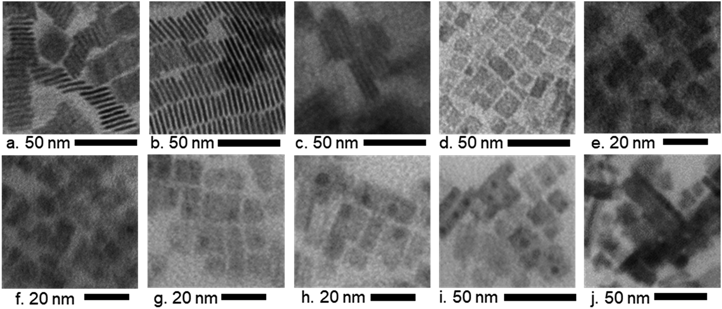 | ||
| Fig. 2 TEM images of (a–e) MAPbBr3 with decreasing ligand concentration (4L, 3.5L, 3L, 2L, and 1L) and (f–j) MAPb(BrxI1−x)3 with increasing iodine content (x = 0.8, x = 0.6, x = 0.5, x = 0.4, and x = 0) and fixed ligands (1L). | ||
UV-visible absorption spectra (Fig. 3) were taken to study the effect of various ligand concentrations and halide compositions on the band gap of the nanocrystals. The absorption spectra of MAPbBr3 with different ligand concentrations are presented in Fig. 3a. We have approximated the band gap using the peak position of the absorption spectra. The absorption spectra of mixed-halide perovskites (‘Br’ and ‘I’) at a fixed ligand concentration are shown in Fig. 3b. These spectra indicate the strong absorption of the synthesized nanocrystals in the visible region. The value of the bandgaps was calculated using Tauc plot analyses which are shown in the inset of Fig. 3b.63 The bandgap ranges from 3.04 eV to 1.51 eV and these values are summarized in Tables 1 and 2. The band gap tuning of MAPbBr3 was achieved through quantum confinement effects in the nanocrystals. The bandgap has a dependence on the ligand concentration while the nanocrystals remain smaller than the Bohr radius size limit because the quantum confinement effect is strongest with smaller nanocrystals and weakens as the size of the nanocrystals increases and disappears completely once the nanocrystals grow larger than the Bohr radius size limit. For mixed halide perovskites, however, the band edge varies via a changing ratio of smaller ‘Br’ ions to larger ‘I’ ions in the crystal structure. It is known that the formation of the bandgap is a result of the bonding interaction between ‘Pb’ and ‘Br/I’ of ABX3 perovskites. The bonding interaction between ‘Pb’ and ‘Br’ is stronger than that between ‘Pb’ and ‘I’.64 Thus, there are larger bandgaps for the perovskites with a high bromine content than that of perovskites containing mostly or entirely iodine. The controllably tuned bandgap energy from violet to IR by using only two types of halide ions leading to successful procurement of colorful optoelectronic devices.
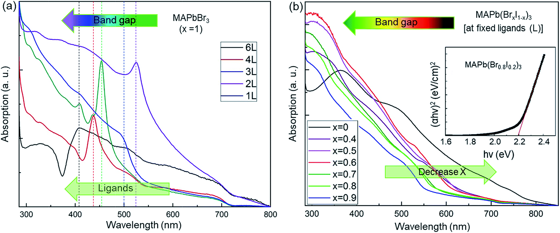 | ||
| Fig. 3 Optical absorption spectra of (a) MAPbBr3 with ligand concentration variation and (b) MAPb(BrxI1−x)3 with ‘Br’ and ‘I’ composition variation at a fixed ligand amount (1L), and inset is the Tauc plot of the sample at x = 0.8. | ||
| Multiple of ligand concentration (L) | Peak emission wavelength (nm) | FWHM (nm) | Band gap (eV) |
|---|---|---|---|
| 1 | 520 | 21 | 2.36 |
| 2 | 510 | 25 | 2.52 |
| 3 | 478 | 26 | 2.73 |
| 3.5 | 458 | 16 | 2.78 |
| 4 | 440 | 15 | 2.83 |
| 6 | 408 | 18 | 3.04 |
| x | Peak emission wavelength (nm) | Lattice parameter (Å) | FWHM (nm) | Band gap (eV) |
|---|---|---|---|---|
| 1 | 520 | 5.930 | 21 | 2.36 |
| 0.9 | 528 | 5.942 | 24 | 2.26 |
| 0.8 | 534 | 5.961 | 35 | 2.19 |
| 0.7 | 562 | 6.004 | 35 | 2.18 |
| 0.6 | 600 | 6.044 | 38 | 2.09 |
| 0.5 | 630 | 6.076 | 41 | 2.00 |
| 0 | 755 | 6.304 | 46 | 1.51 |
Fig. 4 shows the PL emission of MAPb(BrxI1−x)3 perovskites synthesized at various ligand concentrations and different ‘Br’ to ‘I’ ratios. Tunable emission was observed from MAPbBr3 nanocrystals by varying the ligand concentration with an excitation wavelength of 365 nm. The peak position of the PL emission ranged from violet to green (408–520 nm). The ligand concentration affects the PL emission of the nanocrystals by restraining crystal growth as ligands bind to the outside of the nanocrystals during nucleation, thus making the structures smaller. This growth constraint gives rise to stronger quantum confinement effects, thus engineering the PL properties of the material. Then, the ratio of ‘Br’ and ‘I’ was adjusted for MAPb(BrxI1−x)3 at a fixed ligand concentration to obtain wavelength ranges from green to IR (520–755 nm) and these nanocrystals are excited at 450 nm. The peak emission wavelengths are summarized in Tables 1 and 2. The PL emission spectra (violet-IR) are narrow and sharp as characterized by the full-width at half-maximum (FWHM). The range of values for the FWHM from blue to red is 15–41 nm (shown in Tables 1 and 2), which are comparatively smaller values than typically found for these compounds.34,65 The narrow FWHM implies high brightness, strong emission, and color purity in the PL emission of these perovskites which acts to increase the CRI of white light emission.66,67 Hence, we effectively tuned the PL from violet to IR using only two halides in the perovskite nanocrystals.
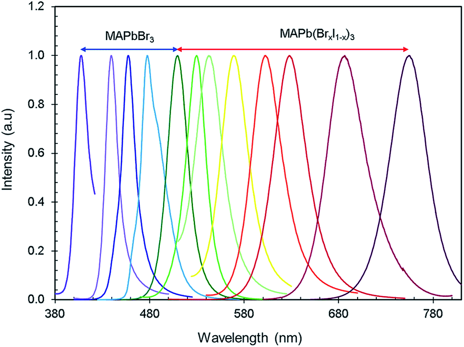 | ||
| Fig. 4 The normalized PL emission spectra of halide perovskite nanocrystals over the range of 408–755 nm with varying ligand concentration for MAPbBr3 and composition of ‘Br’ and ‘I’ for MAPb(BrxI1−x)3. | ||
The FWHM of the PL emission in ligand tuned MAPbBr3 nanocrystals noticeably changes as the spectrum shifts to the red range. The FWHM reduction towards the blue and violet end of the spectrum is due to the effects that ligands have on crystal growth. The shorter crystal growth stage forces all nanocrystals to be smaller in size because there would not be enough time to create a significant size discrepancy between the growing nanocrystals during the shortened crystal growth stage during synthesis. As the ligand concentration decreases, the FWHM of PL emission increases. For mixed-halide perovskites, the increase in the FWHM as the iodine content increases is due to the inherently broader FWHM of MAPbI3 nanocrystals.68
The excitation spectra along with the corresponding emission spectra of the perovskites are shown in Fig. 5. These excitation spectra are broadband and extend from the UV to the visible range, which indicates the possibility of excitation by a wide range of wavelengths. All the nanocrystals synthesized with varying ligand concentrations or anion ratios are therefore usable as down-conversion phosphors on a wide range of III-nitride LEDs for the development of white LED technology.
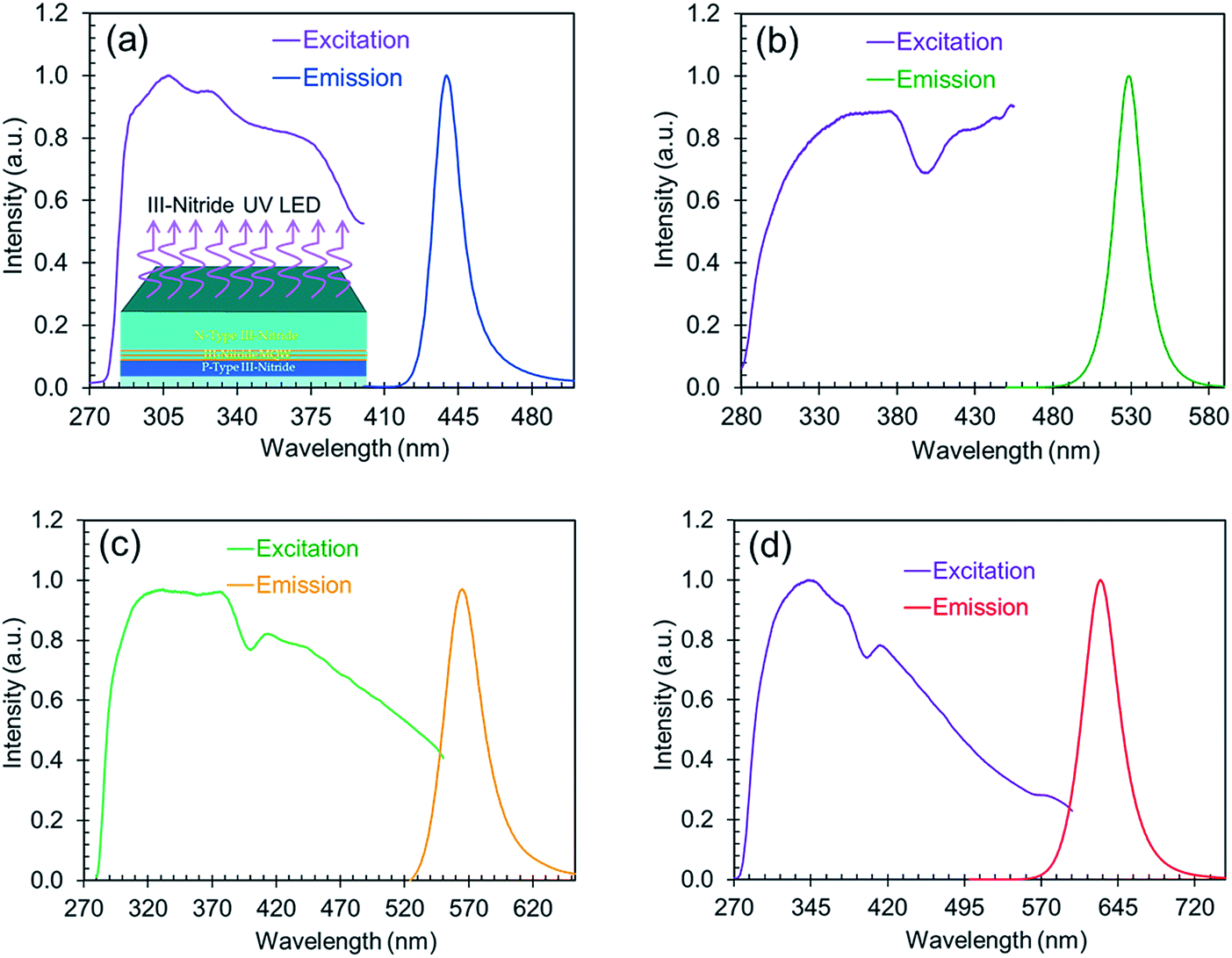 | ||
| Fig. 5 The normalized excitation spectra along with the corresponding normalized emission (blue, green, yellow, and red) spectra. | ||
Furthermore, for the first time, we have demonstrated a strategy to generate high-quality white light emission by combining nanocrystals of blue (λ = 458 nm), green (λ = 510 nm), yellow (λ = 562 nm), and red (λ = 630 nm) emissions. Then, we estimated the CCT and CRI of white light obtained from these nanocrystals. The combined emission spectra, tuned for different CCTs, are presented in Fig. 6. The combination of the four emission spectra demonstrates that a relatively high integrated intensity of the yellow and red phosphors is suitable for warm white light whereas increasing the integrated intensity of blue and green phosphors will cool the light hue. The CIE color coordinate diagram of white light emission is shown in Fig. 7. The effect of tuning the CCT of white light is plotted on the black body curve of the CIE chart. The CIE coordinates corresponding to white light nearly match the Planckian locus, which reveals that the color temperature we obtained is suitable and comfortable for human eyes. Different CCT and CRI values with corresponding CIE coordinates are presented in Table 3. The maximum CRI value we obtained is 93.95 at a CCT of 2759 K. To the best of our knowledge, the CRI value here is superior to previous reports for these materials.3,49 Higher CRI values with suitable CCTs can be obtained from the combination of nanocrystals with different emissions. In addition, one of the CIE coordinates obtained is (0.31, 0.33) which is very close to the standard neutral white light (0.33, 0.33). These results indicate that perovskite nanocrystals MAPb(BrxI1−x)3 have the potential to replace the conventional phosphors for next-generation light emitting devices.
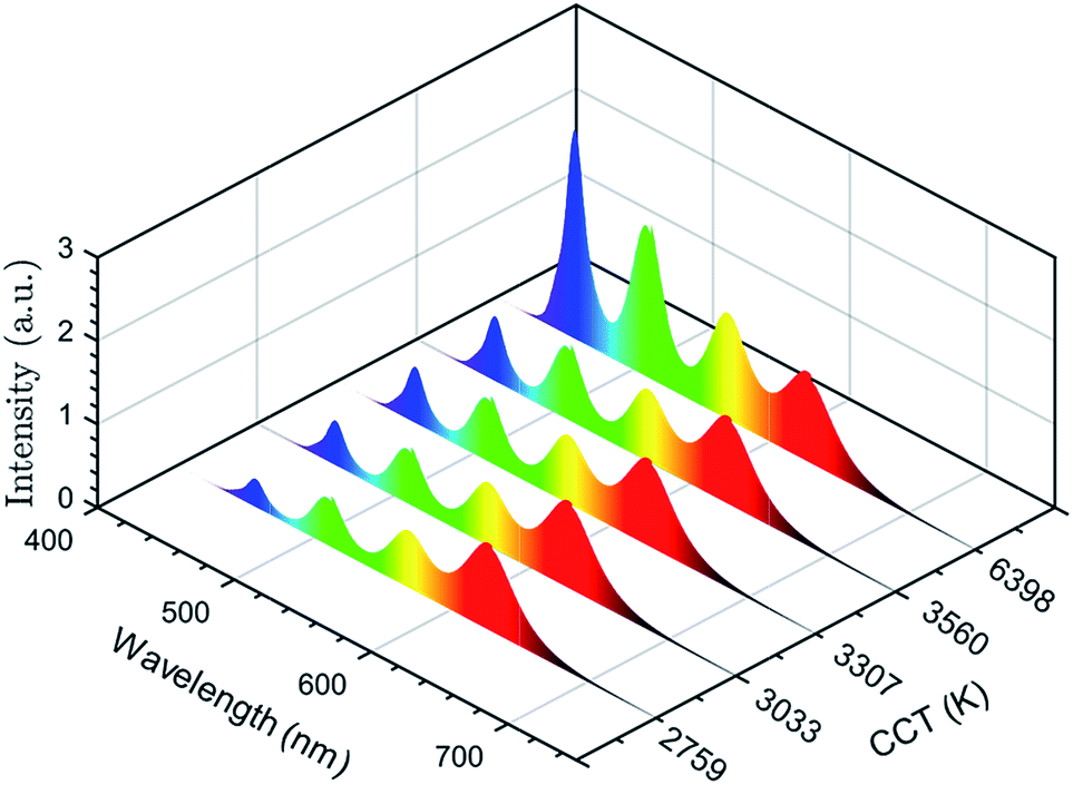 | ||
| Fig. 6 Combination of the emission spectra from four different emissions for tuning the CCT of white light. | ||
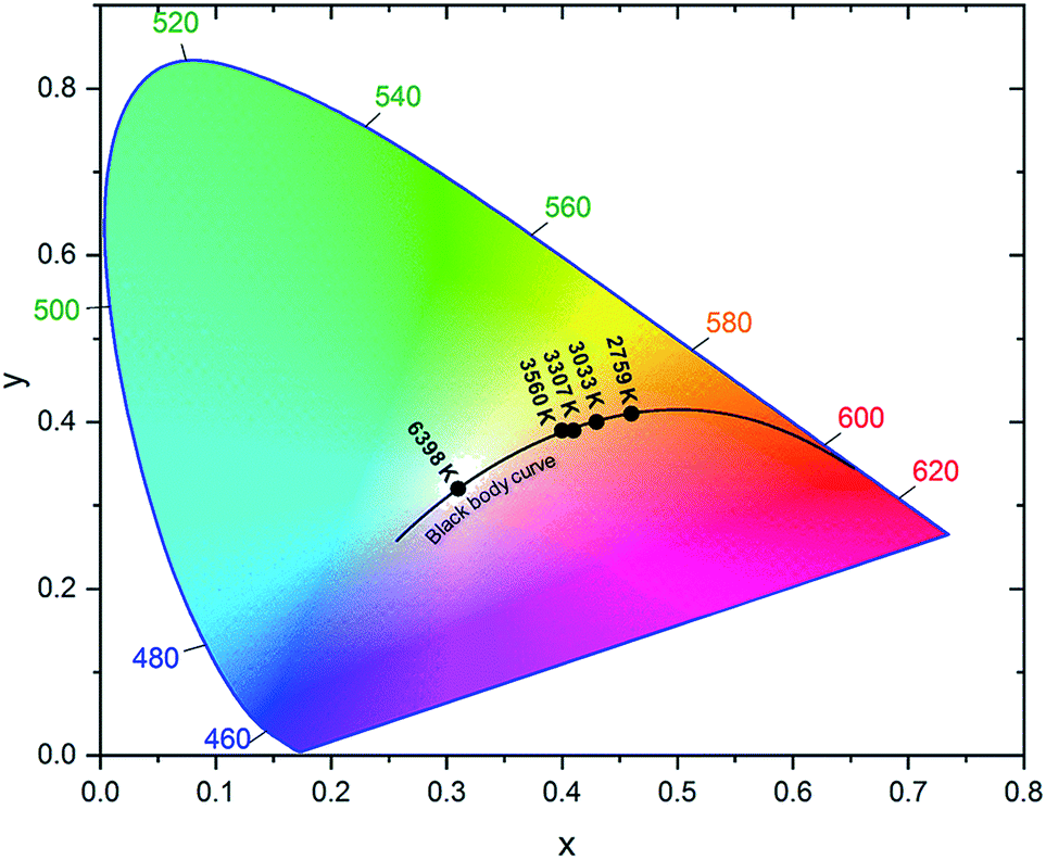 | ||
| Fig. 7 CIE color coordinate diagram showing white light quality across the obtained range of CCT values. | ||
| CCT (K) | Blue | Green | Yellow | Red | CRI | x | y |
|---|---|---|---|---|---|---|---|
| 2759 | 0.15 | 0.34 | 0.45 | 1 | 93.95 | 0.46 | 0.41 |
| 3033 | 0.25 | 0.38 | 0.50 | 1 | 93.71 | 0.43 | 0.40 |
| 3307 | 0.31 | 0.45 | 0.54 | 1 | 93.53 | 0.41 | 0.39 |
| 3560 | 0.36 | 0.52 | 0.58 | 1 | 93.33 | 0.40 | 0.39 |
| 6398 | 1.17 | 1.07 | 0.85 | 1 | 90.59 | 0.31 | 0.33 |
Conclusion
In summary, nanocrystals with PL emission spectra ranging from violet to IR (408–755 nm) have been synthesized by adjusting the ligand concentration in MAPbBr3 and anion ratios of ‘Br’ to ‘I’ in MAPb(BrxI1−x)3 while keeping the ligand concentration constant. The bandgap is controllably tuned through the range of 3.04–1.51 eV. Thus, optoelectronic devices with a broad color gamut are now obtainable using two halide types rather than the traditional three, including MAPbCl3 perovskites. In addition, we have demonstrated, as a first for this class of materials, a CCT estimation extending from cool to warm white emission with CRI values of up to 93.95. To our knowledge, a CRI of 93.95 is the highest value achieved using these materials. This exceptional light quality demonstrates the potential use of this material as the next generation of photon down-conversion phosphors for lighting devices.Conflicts of interest
There are no conflicts to declare.Acknowledgements
The authors acknowledge the financial support by The University of Tulsa through a Start-up Fund. The authors thank Dr Parameswar Harikumar's Semiconductor Characterization Laboratory for allowing the use of equipment for absorption measurements.Notes and references
- M. G. Kibria and Z. Mi, J. Mater. Chem. A, 2016, 4, 2801–2820 RSC.
- N. Guan, X. Dai, A. Messanvi, H. Zhang, J. Yan, E. Gautier, C. Bougerol, F. H. Julien, C. Durand, J. Eymery and M. Tchernycheva, ACS Photonics, 2016, 3, 597–603 CrossRef CAS PubMed.
- J. McKittrick and L. E. Shea-Rohwer, J. Am. Ceram. Soc., 2014, 97, 1327–1352 CrossRef CAS.
- N. Xu Lin, N. Thi Ngoc Nhien, C. Vinh Thang and D. Mau Chien, Adv. Nat. Sci.: Nanosci. Nanotechnol., 2010, 1, 025015 Search PubMed.
- H. Z. Hai Guo, R. F. Wei, M. D. Zheng and LiH. Zhang, Opt. Express, 2011, 19, A201–A206 CrossRef PubMed.
- P. Zhu, H. Zhu, W. Qin, B. H. Dantas, W. Sun, C.-K. Tan and N. Tansu, J. Appl. Phys., 2016, 119, 124305 CrossRef.
- P. F. Smet, K. Korthout, J. E. Van Haecke and D. Poelman, Mater. Sci. Eng., B, 2008, 146, 264–268 CrossRef CAS.
- W. Wang and P. Zhu, Opt. Express, 2018, 26, 34820–34829 CrossRef PubMed.
- P. Zhu, W. Wang, H. Zhu, P. Vargas and A. Bont, IEEE Photonics J., 2018, 10, 4500210 Search PubMed.
- H. Cui, P.-F. Zhu, H.-Y. Zhu, H.-D. Li and Q.-L. Cui, Chin. Phys. B, 2014, 23, 057801 CrossRef.
- T. Guner and M. M. Demir, Phys. Status Solidi A, 2018, 215, 1800120 CrossRef.
- M. M. Lee, J. Teuscher, T. Miyasaka, T. N. Murakami and H. J. Snaith, Science, 2012, 338, 643–647 CrossRef CAS PubMed.
- L. Li, Y. Chen, Z. Liu, Q. Chen, X. Wang and H. Zhou, Adv. Mater., 2016, 28, 9862–9868 CrossRef CAS PubMed.
- L. Zhang, Q. Zeng and K. Wang, J. Phys. Chem. Lett., 2017, 8, 3752–3758 CrossRef CAS PubMed.
- R. Naphade, S. Nagane, G. S. Shanker, R. Fernandes, D. Kothari, Y. Zhou, N. P. Padture and S. Ogale, ACS Appl. Mat. Interfaces, 2016, 8, 854–861 CrossRef CAS PubMed.
- S. Gonzalez-Carrero, R. E. Galian and J. Pérez-Prieto, Opt. Express, 2016, 24, A285–A301 CrossRef CAS PubMed.
- Z. Fan, K. Sun and J. Wang, J. Mater. Chem. A, 2015, 3, 18809–18828 RSC.
- V. A. Hintermayr, A. F. Richter, F. Ehrat, M. Döblinger, W. Vanderlinden, J. A. Sichert, Y. Tong, L. Polavarapu, J. Feldmann and A. S. Urban, Adv. Mater., 2016, 28, 9478–9485 CrossRef CAS PubMed.
- G. C. Adhikari, H. Zhu, P. A. Vargas and P. Zhu, J. Phys. Chem. C, 2018, 122, 15041–15046 CrossRef CAS.
- G. C. Adhikari, P. A. Vargas, H. Zhu and P. Zhu, J. Phys. Chem. C, 2019, 123, 1406–1412 CrossRef CAS.
- S. Gonzalez-Carrero, G. M. Espallargas, R. E. Galian and J. Perez-Prieto, J. Mater. Chem. A, 2015, 3, 14039–14045 RSC.
- Y. Ling, Z. Yuan, Y. Tian, X. Wang, J. C. Wang, Y. Xin, K. Hanson, B. Ma and H. Gao, Adv. Mater., 2016, 28, 305–311 CrossRef CAS PubMed.
- Q. Pan, H. Hu, Y. Zou, M. Chen, L. Wu, D. Yang, X. Yuan, J. Fan, B. Sun and Q. Zhang, J. Mater. Chem. C, 2017, 5, 10947–10954 RSC.
- F. Zhang, H. Zhong, C. Chen, X.-g. Wu, X. Hu, H. Huang, J. Han, B. Zou and Y. Dong, ACS Nano, 2015, 9, 4533–4542 CrossRef CAS PubMed.
- I. Levchuk, A. Osvet, X. Tang, M. Brandl, J. D. Perea, F. Hoegl, G. J. Matt, R. Hock, M. Batentschuk and C. J. Brabec, Nano Lett., 2017, 17, 2765–2770 CrossRef CAS PubMed.
- S. A. Veldhuis, P. P. Boix, N. Yantara, M. Li, T. C. Sum, N. Mathews and S. G. Mhaisalkar, Adv. Mater., 2016, 28, 6804–6834 CrossRef CAS PubMed.
- D. B. Khadka, Y. Shirai, M. Yanagida, T. Noda and K. Miyano, ACS Appl. Mater. Interfaces, 2018, 10, 22074–22082 CrossRef CAS PubMed.
- R. Naphade, B. Zhao, J. M. Richter, E. Booker, S. Krishnamurthy, R. H. Friend, A. Sadhanala and S. Ogale, ACS Appl. Mater. Interfaces, 2017, 4, 1700562 CrossRef.
- E. L. Unger, L. Kegelmann, K. Suchan, D. Sorell, L. Korte and S. Albrecht, J. Mater. Chem. A, 2017, 5, 11401–11409 RSC.
- S. A. Kulkarni, T. Baikie, P. P. Boix, N. Yantara, N. Mathews and S. Mhaisalkar, J. Mater. Chem. A, 2014, 2, 9221–9225 RSC.
- B. J. Bohn, Y. Tong, M. Gramlich, M. L. Lai, M. Döblinger, K. Wang, R. L. Z. Hoye, P. Müller-Buschbaum, S. D. Stranks, A. S. Urban, L. Polavarapu and J. Feldmann, Nano Lett., 2018, 18, 5231–5238 CrossRef CAS PubMed.
- L. Zhang, C. Liu, L. Wang, C. Liu, K. Wang and B. Zou, Angew. Chem., Int. Ed., 2018, 57, 11213–11217 CrossRef CAS PubMed.
- Y. Tong, M. Fu, E. Bladt, H. Huang, A. F. Richter, K. Wang, P. Müller-Buschbaum, S. Bals, P. Tamarat, B. Lounis, J. Feldmann and L. Polavarapu, Angew. Chem., Int. Ed., 2018, 57, 16094–16098 CrossRef CAS PubMed.
- J. Xing, F. Yan, Y. Zhao, S. Chen, H. Yu, Q. Zhang, R. Zeng, H. V. Demir, X. Sun, A. Huan and Q. Xiong, ACS Nano, 2016, 10, 6623–6630 CrossRef CAS PubMed.
- Z.-K. Tan, R. S. Moghaddam, M. L. Lai, P. Docampo, R. Higler, F. Deschler, M. Price, A. Sadhanala, L. M. Pazos, D. Credgington, F. Hanusch, T. Bein, H. J. Snaith and R. H. Friend, Nat. Nanotechnol., 2014, 9, 687–692 CrossRef CAS PubMed.
- X. Qin, H. Dong and W. Hu, Sci. China Mater., 2015, 58, 186–191 CrossRef CAS.
- H. Zhu, T. Cai, M. Que, J.-P. Song, B. M. Rubenstein, Z. Wang and O. Chen, J. Phys. Chem. Lett., 2018, 9, 4199–4205 CrossRef CAS PubMed.
- H. Shao, X. Bai, H. Cui, G. Pan, P. Jing, S. Qu, J. Zhu, Y. Zhai, B. Dong and H. Song, Nanoscale, 2018, 10, 1023–1029 RSC.
- T. Li, Y. Pan, Z. Wang, Y. Xia, Y. Chen and W. Huang, J. Mater. Chem. A, 2017, 5, 12602–12652 RSC.
- D. B. Khadka, Y. Shirai, M. Yanagida and K. Miyano, J. Mater. Chem. C, 2018, 6, 162–170 RSC.
- S. Pont, D. Bryant, C.-T. Lin, N. Aristidou, S. Wheeler, X. Ma, R. Godin, S. A. Haque and J. R. Durrant, J. Mater. Chem. A, 2017, 5, 9553–9560 RSC.
- A. Polman, M. Knight, E. C. Garnett, B. Ehrler and W. C. Sinke, Science, 2016, 352, 4424 CrossRef PubMed.
- P. Wangyang, H. Sun, X. Zhu, D. Yang, X. Gao, W. Liu, Y. Chen, H. Tian and S. Huanglong, Phys. Status Solidi A, 2017, 214, 1700538 CrossRef.
- L. Li, Z. Sun, P. Wang, W. Hu, S. Wang, C. Ji, M. Hong and J. Luo, Angew. Chem., Int. Ed., 2017, 56, 12150–12154 CrossRef CAS PubMed.
- J. Zhang, X. Yang, H. Deng, K. Qiao, U. Farooq, M. Ishaq, F. Yi, H. Liu, J. Tang and H. Song, Nano-Micro Lett., 2017, 9, 36 CrossRef PubMed.
- Z. Gu, K. Wang, W. Sun, J. Li, S. Liu, Q. Song and S. Xiao, Adv. Opt. Mater., 2016, 4, 472–479 CrossRef CAS.
- Y. En-Ping, Y. Zhanlue, M. Lei, S. Pengyu, D. Shiqi, Y. Ye and Y. Yang, Adv. Mater., 2017, 29, 1606859 CrossRef PubMed.
- K. T. Shimizu, M. Böhmer, D. Estrada, S. Gangwal, S. Grabowski, H. Bechtel, E. Kang, K. J. Vampola, D. Chamberlin, O. B. Shchekin and J. Bhardwaj, Photonics Res., 2017, 5, A1–A6 CrossRef CAS.
- S. Pathak, N. Sakai, F. Wisnivesky Rocca Rivarola, S. D. Stranks, J. Liu, G. E. Eperon, C. Ducati, K. Wojciechowski, J. T. Griffiths, A. A. Haghighirad, A. Pellaroque, R. H. Friend and H. J. Snaith, Chem. Mater., 2015, 27, 8066–8075 CrossRef CAS.
- Y.-W. Zhang, G. Wu, H. Dang, K. Ma and S. Chen, Ind. Eng. Chem. Res., 2017, 56, 10053–10059 CrossRef CAS.
- E. R. Dohner, A. Jaffe, L. R. Bradshaw and H. I. Karunadasa, J. Am. Chem. Soc., 2014, 136, 13154–13157 CrossRef CAS PubMed.
- L. Mao, Y. Wu, C. C. Stoumpos, M. R. Wasielewski and M. G. Kanatzidis, J. Am. Chem. Soc., 2017, 139, 5210–5215 CrossRef CAS PubMed.
- Z. Zhuang, C. Peng, G. Zhang, H. Yang, J. Yin and H. Fei, Angew. Chem., Int. Ed., 2017, 56, 14411–14416 CrossRef CAS PubMed.
- C. Peng, Z. Zhuang, H. Yang, G. Zhang and H. Fei, Chem. Sci., 2018, 9, 1627–1633 RSC.
- R. K. Misra, L. Ciammaruchi, S. Aharon, D. Mogilyansky, L. Etgar, I. Visoly-Fisher and E. A. Katz, ChemSusChem, 2016, 9, 2572–2577 CrossRef CAS PubMed.
- T. Baikie, Y. Fang, J. M. Kadro, M. Schreyer, F. Wei, S. G. Mhaisalkar, M. Graetzel and T. J. White, J. Mater. Chem. A, 2013, 1, 5628–5641 RSC.
- L.-d. Tang, H. Mei, B. Wang and S. Peng, J. Mater. Sci.: Mater. Electron., 2015, 26, 8726–8731 CrossRef CAS.
- J. H. Noh, S. H. Im, J. H. Heo, T. N. Mandal and S. I. Seok, Nano Lett., 2013, 13, 1764–1769 CrossRef CAS PubMed.
- Y. Nagaoka, K. Hills-Kimball, R. Tan, R. Li, Z. Wang and O. Chen, Adv. Mater., 2017, 29, 1606666 CrossRef PubMed.
- Y. Nagaoka, R. Tan, R. Li, H. Zhu, D. Eggert, Y. A. Wu, Y. Liu, Z. Wang and O. Chen, Nature, 2018, 561, 378–382 CrossRef CAS PubMed.
- Q. A. Akkerman, S. G. Motti, A. R. Srimath Kandada, E. Mosconi, V. D'Innocenzo, G. Bertoni, S. Marras, B. A. Kamino, L. Miranda, F. De Angelis, A. Petrozza, M. Prato and L. Manna, J. Am. Chem. Soc., 2016, 138, 1010–1016 CrossRef CAS PubMed.
- O. Vybornyi, S. Yakunin and M. V. Kovalenko, Nanoscale, 2016, 8, 6278–6283 RSC.
- B. P. Kafle, S. Acharya, S. Thapa and S. Poudel, Ceram. Int., 2016, 42, 1133–1139 CrossRef CAS.
- Y. Heng-Yun, L. Wei-Qiang, H. Chun-Li, Z. Yi, Y. Yu-Meng, M. Jiang-Gao, L. Peng-Fei and X. Ren-Gen, Adv. Mater., 2016, 28, 2579–2586 CrossRef PubMed.
- G. Li, F. W. R. Rivarola, N. J. L. K. Davis, S. Bai, T. C. Jellicoe, F. de la Peña, S. Hou, C. Ducati, F. Gao, R. H. Friend, N. C. Greenham and Z.-K. Tan, Adv. Mater., 2016, 28, 3528–3534 CrossRef CAS PubMed.
- G. Li, Z.-K. Tan, D. Di, M. L. Lai, L. Jiang, J. H.-W. Lim, R. H. Friend and N. C. Greenham, Nano Lett., 2015, 15, 2640–2644 CrossRef CAS PubMed.
- S. Zhuang, X. Ma, D. Hu, X. Dong and B. Zhang, Ceram. Int., 2018, 44, 4685–4688 CrossRef CAS.
- D. Li, G. Wang, H.-C. Cheng, C.-Y. Chen, H. Wu, Y. Liu, Y. Huang and X. Duan, Nat. Commun., 2016, 7, 11330 CrossRef CAS PubMed.
| This journal is © The Royal Society of Chemistry 2019 |