
 Open Access Article
 This Open Access Article is licensed under a
 Creative Commons Attribution 3.0 Unported Licence
Solution based CVD of main group materials
Caroline E.
Knapp
and
Claire J.
Carmalt
*
Department of Chemistry, University College London, 20 Gordon Street, London WC1H 0AJ, UK. E-mail: c.j.carmalt@ucl.ac.uk
First published on 8th October 2015
Abstract
This critical review focuses on the solution based chemical vapour deposition (CVD) of main group materials with particular emphasis on their current and potential applications. Deposition of thin films of main group materials, such as metal oxides, sulfides and arsenides, have been researched owing to the array of applications which utilise them including solar cells, transparent conducting oxides (TCOs) and window coatings. Solution based CVD processes, such as aerosol-assisted (AA)CVD have been developed due to their scalability and to overcome the requirement of suitably volatile precursors as the technique relies on the solubility rather than volatility of precursors which vastly extends the range of potentially applicable compounds. An introduction into the applications and precursor requirements of main group materials will be presented first followed by a detailed discussion of their deposition reviewed according to this application. The challenges and prospects for further enabling research in terms of emerging main group materials will be discussed.
 Caroline E. Knapp | Caroline Knapp gained her MSci and then PhD from UCL in the field of precursor design and analysis with Professors Claire Carmalt and Paul McMillan. Following this she worked on low valent group 14 chemistry at UC Davis, CA, with Professor Phil P. Power. She returned to the UK, firstly with a post doc. at Imperial College under the supervision of Dr. Joachim Steinke and secondly back at UCL, under the supervision of Professors Carmalt and Ivan Parkin. She was awarded a Ramsay Fellowship in 2015 and now carries out research isolating novel precursors for the printing of electronic devices. |
 Claire J. Carmalt | Claire Carmalt is a Professor of Inorganic Chemistry at University College London (UCL). She is currently the Head of the Inorganic & Materials section and Vice Dean (Education), Mathematical & Physical Sciences Faculty. She obtained her BSc and PhD from the University of Newcastle upon Tyne and was a postdoctoral fellow at the University of Austin at Texas. She has published over 190 research papers and 10 reviews/contributions to books. Her group's research involves the development of innovative new routes to technologically important inorganic materials focusing on the synthesis of “designed” molecular precursors and Aerosol Assisted Chemical Vapour Deposition. |
1 Introduction
Thin films incorporating main group elements play a critical role in many current and potential applications. This is particularly true for electronic applications with semiconductors based on combinations of elements from Groups III and V, III and VI, II and VI and IV and VI having significant impact on our every day lives. These materials, including gallium nitride (GaN), gallium arsenide (GaAs) and copper indium gallium selenide (CIGS) are utilised in a wide range of applications in solar cells, satellite TV receivers, optical fibre communications and full colour advertising displays. Similarly, transparent conducting oxides (TCOs) play a key role in many optoelectronic devices due to their unique combination of transparency in the visible region of the spectrum and electrical conductivity. These metal oxide thin films, dominated by main group oxides like indium tin oxide (ITO) and fluorine-doped tin oxide (FTO), are ideal for applications in displays and photovoltaics. There is an increasing demand for new materials and cost-effective methods of depositing these materials while minimising environmental impact, to align with the current rapid growth of these industries.These materials are currently used in the form of thin films and a variety of methods have been employed to deposit these films including chemical vapour deposition (CVD), atomic layer deposition (ALD), spin coating and sol–gel methods. The most common method to thin films is CVD, which can be used to deposit on small scale coatings, such as microelectronics and larger areas of growth, for example glass/steel coatings.1 Due to a large variety of variables and different types of CVD, the properties of the thin films can be fine-tuned and good film uniformity and compositional control is possible. However, both the composition and structure of the deposited materials can be significantly effected by the nature and purity of the precursors. Generally, it is important to have volatile precursors for use in CVD and the reaction chemistry can be complex. Aerosol-assisted (AA)CVD is a solution-based process, which relies on the solubility rather than volatility, of the precursor.2 In the AACVD process, precursors are dissolved in a solvent from which an aerosol is generated via the use of an ultrasonic humidifier/nebulizer, which creates a ‘precursor mist’, which can then be transported to the CVD reactor by a carrier gas. The transport of aerosol droplets, rather than relying on the evaporation of volatile precursors in order to transport precursors to the reaction chamber, is a key advantage of AACVD. The process is scalable, allows for the formation of multicomponent materials and the simplification of the precursor delivery stage potentially reduces the cost of the deposition process. The particle size and morphology of the deposited film can be closely controlled by the deposition temperature, choice of solvent and controlling the frequency of the ultrasonic modulator. As such CVD has been used in the production of nanomaterials with tailored features.3–5 The formation of thin films via AACVD is the result of homogeneous or heterogeneous reaction or a combination of both homogeneous nucleation in the gas phase and heterogeneous growth on the substrates.
This review examines the use of AACVD as a method for the deposition of thin films of main group materials. The influence of precursors utilised and deposition conditions employed on film characteristics is discussed and applications to which AACVD has been found beneficial will be highlighted. This review aims to summarise recent achievements of AACVD in the preparation of these main group materials, and to present some ideas regarding future prospects. The review is organised to provide an overview of the deposition of thin films of main group materials, grouped according to their application. The importance of morphological control, from the selection of precursors used to deposition conditions chosen is key for best performance in the targeted technological applications; which are discussed in the order: main group semiconductors, TCOs, PEC materials and gas sensors.
2 Overview of precursor requirements
In order to limit potential contamination in deposited thin films a crucial requirement for a precursor is its purity. Hence, development of precursors requires investigation into purification techniques and potentially alternative synthetic routes to achieve highly pure compounds. For scale up and use in industry, the precursor must be able to be prepared and isolated readily in large quantities, and with minimal environmental or cost implications. Stability and low toxicity of the precursor are also important for ease of use and storage.CVD processes traditionally involved the use of dual source precursors but efforts to lower the growth temperature resulted in the development of single-source precursors, which already contain an M–E (e.g. M = group 12, 13, 14 element; E = N, P, As, Sb, S, Se etc.) bond at the core of the molecule, with various other ligands attached to each of the elements. The desired reaction pathway involves adsorption of the precursor without breaking the M–E bond but with loss of the ancillary ligands. Single-source precursors potentially display a range of advantages over conventional CVD precursors, including:
– Limited pre-reaction as there is only one precursor.
– Reduced toxicity (e.g. for III–V materials AsH3, PH3 are eliminated from the CVD process).
– Possible lower temperature growth.
– Air and moisture stability is possible.
However, commercialisation of single-source precursors are still limited due to their disadvantages, including:
– Difficulties in control of stoichiometry using single-source precursors, such as in the growth of ternary and quaternary materials, for example InxGa1−xAsx.
– Low volatility, such that the use of established MOCVD equipment is difficult.
– Low surface mobility of polynuclear decomposition fragments can prevent epitaxial growth.
During CVD, it is necessary for the precursor to decompose at elevated temperatures on the surface of a substrate, such as glass, to result in deposition of the required thin film. Typically, therefore, volatility is very important such that the precursor will be readily volatile at temperatures below its decomposition to yield high quality thin films. The development of solution based CVD routes has meant that the requirement of volatility of precursors has been overcome as these techniques rely on solubility of the precursor rather than volatility. This vastly extends the range of potentially applicable compounds for use as precursors to thin films. AACVD is a solution based technique that has generated much interest in the deposition of a wide range of films. In the AACVD process a nebulizer is used to form aerosol droplets of the precursor solution to transport precursors to the reaction chamber using a carrier gas (Fig. 1). On reaching the substrate, evaporation of the solvent occurs due to the increase in temperature. Hence, the vapourised precursor is then in its gaseous state and deposition onto the substrate can occur to yield the desired material. An advantage of AACVD is that the requirement to isolate and purify a precursor, as required in conventional CVD processes, is not always necessary and the precursor can be synthesised in situ in the solution being used in the AACVD process. Furthermore, simply mixing different precursors in the solution used within the AACVD process has enabled deposition of ternary materials. Therefore, AACVD has eliminated many of the disadvantages traditionally associated with single-source precursors (volatility, control of stoichiometry). The conditions applied during deposition in an AACVD process can greatly affect the microstructure of the film with the morphology of the deposited films depending on a range of factors, including temperature, solvent, substrate and the precursor.
 | ||
| Fig. 1 Schematic illustration of the process involved in AACVD. | ||
3 Main group semiconductors
Informative reviews of the growth techniques and structural, electrical and optical properties as well as applications of semiconductors have been published by Malik et al.,6 Ambacher,7 Strite et al.,8 and Jones and O'Brien.9 Applications of semiconductors include in solar cells, light emitting diodes, photocathodes, lasers and thermal imaging devices. Volatile organometallic compounds have been increasingly used for the deposition of compound semiconductors. Metalorganic chemical vapour deposition (MOCVD) is commonly used for the formation of semiconductors using organometallic precursors.2 This process either uses a dual- or single-source precursor system. The progress of techniques of this type has been the result of developments in precursor chemistry including improved synthesis and purification. One of the driving forces in recent years in the organometallic chemistry of group 13 (Al, Ga, In) has been their increased use in the electronics industry, for example semiconducting III–V materials such as GaAs, GaN and InP. Other semiconductors formed using organometallic precursors include chalcogenides (SnS, In2S3), and ternary phases (CuInSe2). In this section the development of precursors for compound semiconductors for use in AACVD is described.3.1 Groups 12 and 16 (II–VI) thin films
The intermediate energy band gaps of II–VI semiconductors has led to their use in a variety of devices.10 For example, cadmium chalcogenides have applications in solid-state solar cells, in light-emitting diodes for flat-panel displays, sensors and in field-effect transistors. The Zn- and Cd-based chalcogenides (ZnS, ZnSe, CdS, CdSe and CdTe) have been grown by conventional MOCVD from dimethyl-cadmium or -zinc in combination with H2S, H2Se or Me2Te11 and from single-source precursors.2 Low temperature growth is important because these II–VI materials interdiffuse and form defects at temperatures above 500 °C. To reduce toxicity and the growth temperature and control the purity of the films deposited new precursors have been developed. For example, mixed alkyl/dithio- or diseleno-carbamates and xanthanates12–16 are potential precursors to II–VI materials as they provide access to lower deposition temperatures and zinc selenide, cadmium sulfide and cadmium selenide thin films have been deposited from compounds, of the type [RM(E2CNEt2)]2 (M = Zn, Cd, E = S, Se, R = Me, CH2CMe3)17via MOCVD. Reviews by Gleizes18 and O'Brien2,19 provide detailed accounts on the use of other single-source precursors for the deposition of chalcogenide materials by MOCVD. Complexes of this type were expected to be relatively unstable and have low volatility. However, a wide range of compounds have been used in AACVD processes to produce II–VI thin films (vide infra). Thin films of these materials have also been deposited by other solution based methods such as spray pyrolysis,20,21 spin coating,22 electrostatic assisted aerosol jet deposition,23 chemical bath deposition24,25 and solution growth.26AACVD of CdS, ZnS and Cd1−xZnxS films was originally reported by Hampden-Smith et al. utilising precursors, of the type [M(SOCMe)2(tmeda)] (where tmeda = N,N,N,N-tetramethylethylenediamine).27,28 AACVD was the chosen CVD technique to aid with the delivery of precursors with lower volatility and ease of handling of highly reactive precursors. The zinc compound, [Zn(SOCMe)2(tmeda)] was prepared via reaction of ZnEt2 with two equivalents of HSOCMe and 1 equivalent of tmeda, whereas the Cd species was isolated from the reaction of Cd(CO3) with HSOCMe and one equivalent of tmeda. The compounds were found to be monomeric and isostructural in the solid state with both possessing S-bonded thioacetate ligands. The coordination environment of the metal atoms in both compounds was a distorted tetrahedral comprising two nitrogen atoms and two sulfur atoms. Decomposition of the compounds was observed to proceed via thermally induced thioacetic anhydride elimination, as shown in eqn (1).
| M(SOCMe)2(tmeda) → MS + S(OCMe)2 + tmeda | (1) |
![[thin space (1/6-em)]](https://www.rsc.org/images/entities/char_2009.gif) :Zn ratios of 6:4, 5:5, 4:6 and 2.5:7.5. The deposited films were found to have similar growth rates and morphologies as the individual ZnS and CdS films and adopted a (002)-orientated hexagonal phase. Binary phases of ZnS and CdS were not observed by X-ray diffraction but a general trend was found where the films were Cd deficient compared to the solutions by ∼5–10 at%.
:Zn ratios of 6:4, 5:5, 4:6 and 2.5:7.5. The deposited films were found to have similar growth rates and morphologies as the individual ZnS and CdS films and adopted a (002)-orientated hexagonal phase. Binary phases of ZnS and CdS were not observed by X-ray diffraction but a general trend was found where the films were Cd deficient compared to the solutions by ∼5–10 at%.
More recently, thin films of CdS, ZnS and Cd1−xZnxS have been deposited by AACVD using thio- and dithio-biuret zinc and cadmium precursors, of the type [M{(SCNR2)2N}2] (M = Zn, Cd, R = Me, Et) and [M(SON(CNiPr2)2)2] (M = Zn, Cd).29,30 The ligands and precursors were synthesised as shown in Scheme 1. Reaction of sodium thiocyanate, N,N′-dialkylcarbamyl chloride and the relevant dialkylamine produced the 1,1,5,5-tetraalky-l-2-thiobiuret ligand. The metal complexes were formed by addition of the corresponding metal acetate in methanol to the ligand. A similar synthetic route was followed to isolate dithiobiuret complexes starting from N,N′-dialkylthiocarbamylchloride. Single crystal X-ray diffraction showed that the zinc or cadmium atom in the precursor adopted a distorted tetrahedral geometry. Thermogravimetric analysis (TGA) indicated that the zinc and cadmium precursors decomposed to the corresponding metal sulfides at similar temperatures. AACVD of [Zn{(SCNR2)2N}2] (R = Me, Et) and [Zn{SON(CNiPr2)2}2] in THF afforded cubic ZnS films with small rods and granular crystallites at 300 and 350 °C but hexagonal ZnS with granular crystallites at 400 and 450 °C. Likewise, the corresponding cadmium precursors resulted in the deposition of hexagonal granular CdS films at all deposition temperatures. By varying the molar ratio of Zn:Cd compounds in the precursor mixture, ternary films of Cd1−xZnxS were deposited at 400 °C. The formation of a solid solution was confirmed by powder X-ray diffraction (XRD), energy dispersive X-ray (EDAX) spectroscopy and UV-vis. The optical band gap for the ZnS films was found to be 3.35 eV, for CdS 2.39 eV and for the ternary material Cd1−xZnxS ranged from 3.10–2.52 eV depending on the value of x (x = 0.25, 0.50, 0.75). In general, the band gap was found to increase with increasing temperature, as expected. Overall, pairs of precursors resulted in the deposition of homogeneous Cd1−xZnxS films, which is largely the result of the zinc and cadmium precursors decomposing at similar temperature in a single step. Thio- and dithio-biurets have also been explored for the synthesis of other metal complexes and deposition of materials including Co, Ni, Fe, In, and Cu.20,31
 | ||
| Scheme 1 Synthesis of thio- and dithio-biuret zinc and cadmium precursors. | ||
A cadmium complex of dimorpholinodithioacetylacetonate (msacmsac) has been used as a single-source precursor for the deposition of CdS films by AACVD.32 The ligand msacmsac was prepared by the reaction of morpholine with sulfur and allyl propyl ether at 110 °C for several hours. Subsequent reaction of the ligand with cadmium nitrate resulted in the isolation of the cadmium complex, [Cd(msacmsac)2(NO3)2]. The structure of the complex shows a bidentate coordination by the sulfur atoms of each ligand to the cadmium metal and an overall octahedral coordination geometry, as shown in Fig. 2. AACVD of [Cd(msacmsac)2(NO3)2] in dimethylformamide and chloroform (1:1) was carried out at 450 and 500 °C. As expected, thicker films were deposited at the higher temperature and powder XRD indicated that hexagonal CdS had been deposited.
 | ||
| Fig. 2 Molecular structure of [Cd(msacmsac)2(NO3)2] with thermal ellipsoids plotted at the 50% probability. Reproduced from ref. 32 with permission from The Royal Society of Chemistry. | ||
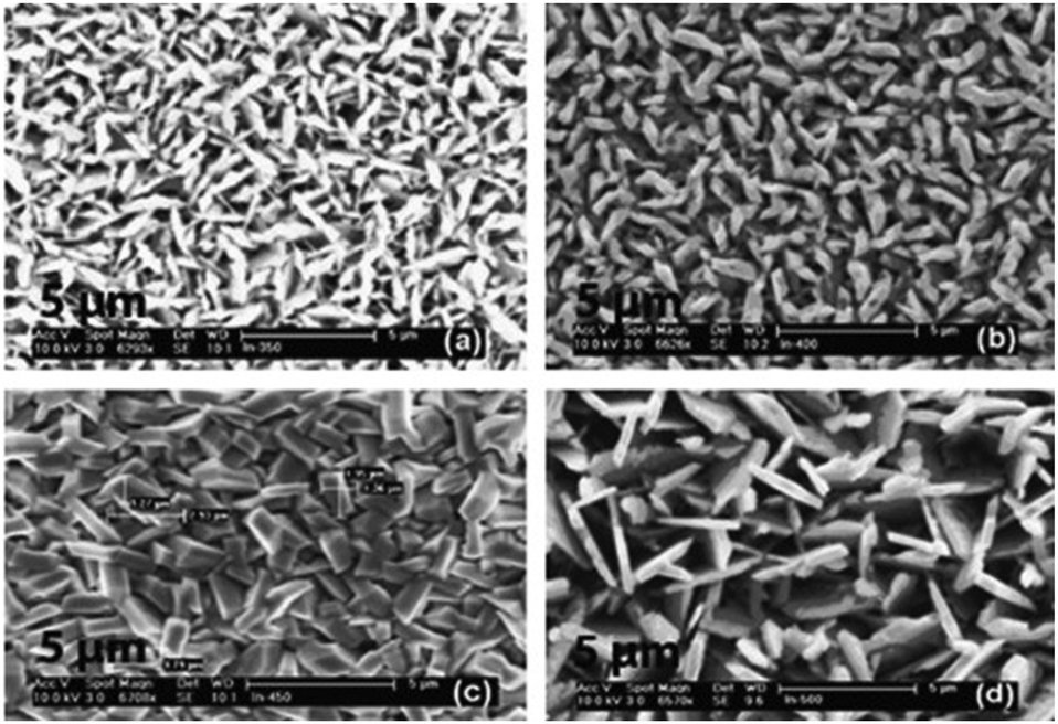
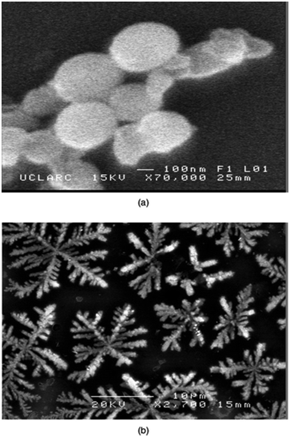
Dithiocarbamates are chelating ligands that form stable complexes with most elements.33,34 As mentioned above, a number of dithiocarbamate precursors have been used for the deposition of metal chalcogenide thin films via MOCVD.11 In addition, several adducts of cadmium dithiocarbamate complexes were reported but their capabilities as precursors for CVD were not described.35,36 The formation of adducts was investigated in order to produce precursor molecules with adequate volatility since the addition of a Lewis base decreases the degree of association present in a polymeric structure by forming monomeric complexes. However, they have also been found to meet all the necessary requirements of a precursor for the fabrication of thin films by AACVD. The cadmium dithiocarbamate complex, [Cd(S2CNCy2)2·py] (Cy = cyclohexyl, py = pyridine) has been used to deposit CdS nanostructured thin films on soda and FTO conducting glass substrates by AACVD in toluene, THF and pyridine solutions at 350–450 °C.37 The complex, [Cd(S2CNCy2)2·py] was shown by single crystal X-ray diffraction to be monomeric with a distorted square pyramidal geometry around the Cd atom. The formation of hexagonal CdS thin films resulted from all depositions using [Cd(S2CNCy2)2·py] regardless of the solvent or temperature employed. Thin films of CdS with a variety of morphologies and particle sizes could be formed depending on the temperature and also solvent used since the physical properties of the solvent (e.g. boiling point, viscosity, coordination ability etc.) has a marked effect. This is illustrated in Fig. 3 which shows the varied morphology obtained from THF solutions at the various temperatures. For all solvents (pyridine, THF and toluene) selective nanostructures, such as shown in Fig. 3a, were only produced on the conducting FTO substrate and not soda lime. This is a result of the charged aerosol droplets undergoing evaporation causing the electric charge density to increase with the shrinking of the droplet.38 Due to intense repulsion by the conducting substrate multiple fine particles are selectively formed and absorbed on the substrate where the growing process yields the nanostructures.
 | ||
| Fig. 3 SEM images of CdS thin films deposited from [Cd(S2CNCy2)2·py] on FTO (a–c) and soda glass (d–f) at 350, 400, and 450 °C from THF solution. Reproduced with permission from ref. 37. Copyright 2012 Wiley. | ||
AACVD of the related zinc complexes, [Zn(S2CNCy2)2·py] and [Zn(S2CN(CH2Ph)Me)2·py] in toluene at 375, 425 and 475 °C, has also been reported.39 In general, ZnS crystallises into two structural polymorphs, cubic (sphalerite) and hexagonal (wurtzite), and phase selectivity is influenced by the precursor, deposition technique, substrate and processing parameters. Using these precursors in AACVD it was found that at the lower temperature of 375 °C the cubic phase was dominant with the hexagonal phase present as a minority phase. At the higher temperature of 475 °C the hexagonal phase was observed as the major phase with some cubic phase present. SEM showed that the surface morphology of the ZnS films deposited was strongly dependent on the nature of the precursor as well as the deposition temperature. For example, using [Zn(S2CNCy2)2·py], films deposited at 375 °C consisted of well-orientated cauliflower-like structures, whereas unstructured particles were formed from [Zn(S2CN(CH2Ph)Me)2·py] at the same temperature. The band gaps of the films deposited at 475 °C from [Zn(S2CNCy2)2·py] and [Zn(S2CN(CH2Ph)Me)2·py] were 3.36 and 3.40 eV, respectively corresponding well with that expected for hexagonal ZnS.
Recently, the pyridine adduct of bis(piperidine dithiocarbamato)cadmium(II), [Cd(S2CNC5H10)2·py] was evaluated as a single-source precursor for the deposition of CdS films.40 AACVD of [Cd(S2CNC5H10)2·py] in chloroform at 350–450 °C deposited thin films of hexagonal CdS with band gaps of ∼2.6 eV. Again the temperature of deposition was found to affect the resulting morphology of the film, as shown in Fig. 4. At the lower temperature of 350 °C the CdS films had regular hexagonal-like domains whereas at 450 °C close to spherical granules were observed. The deposition temperature was observed to modify the grain sizes as well as the surface roughness. These precursors were also used to synthesize CdS nanoparticles.
 | ||
| Fig. 4 SEM images of CdS thin films deposited from [Cd(S2CNC5H10)2·py] at (a) 350 °C; (b) 400 °C and (c) 450 °C. Reproduced from ref. 40 with permission from the Centre National de la Recherche Scientifique (CNRS) and the Royal Society of Chemistry. | ||
Thin films of ZnS and CdS have also been deposited from [M(S2CNnBu2)2] (M = Zn, Cd) via AACVD in toluene at 350–450 °C on soda glass substrates.41,42 For ZnS, no deposition was observed at 350 °C but at higher temperatures hexagonal ZnS was deposited with a rod-like structure. Thin films of hexagonal CdS could be deposited at 350 °C, which consisted of densely packed granular crystallites whereas at higher temperatures the morphology changes to a flake-like structure.
AACVD of CdS and CdTe has been carried out using [Cd{(SPiPr2)2N}2] and [Cd{(TePiPr2)2N}2] in toluene at substrate temperatures between 550–550 °C and 375–475 °C, respectively.43,44 AACVD of [Cd{(SPiPr2)2N}2] resulted in the formation of hexagonal CdS at deposition temperatures of 500 °C but growth of cubic Cd6P7 and orthorhombic Cd7P10 at 525 °C. SEM of the CdS films grown at 500 °C showed that they were composed of dense, ribbon-like primary crystallites. Synthesis of the CdTe precursor, [Cd{(TePiPr2)2N}2] could not be achieved by direct reaction of NH(PiPr2)2 with tellurium. An alternative approach involved metalation of NH(PiPr2)2 with NaH prior to reaction with tellurium, which facilitated the formation of Na[N(TePiPr2)2] which was then reacted with CdCl2. AACVD of [Cd{(TePiPr2)2N}2] resulted in the formation of a mixture of cubic CdTe and hexagonal Te at 375 °C and pure cubic CdTe films at 475 °C with preferred orientation along (111) direction. Under similar conditions, AACVD of [Hg{(TePiPr2)2N}2] resulted in the deposition of hexagonal tellurium, which may be due to reductive elimination of mercury at higher temperatures.41 Related complexes have also been used to form CuTe, Ag7Te4 and AuTe2 films.45
Bis-chelates of cadmium, of the type [Cd{iPr2P(X)NC(Y)NC4H8-η2-S,O}] (X = S, Y = O; X = O, Y = S), have been used as single-source precursors for the deposition of thin films via AACVD.46 Preliminary AACVD studies at 400 and 500 °C indicated that metal-enriched CdS formed with a high degree of carbon contamination from the precursor containing a P![[double bond, length as m-dash]](https://www.rsc.org/images/entities/char_e001.gif) O group.
O group.
3.2 Groups 13 and 15 (III–V) thin films
The conventional approach to growing III–V thin films is where separate group III and V precursors are combined. The metalorganic precursors traditionally employed are readily available commercially and have convenient vapour pressures. Manasevit first described the use of organometallic compounds to deposit III–V films in 1968,47 and these original precursors are still favoured today. The volatile group III trialkyls, such as trimethylaluminum (AlMe3), trimethylgallium (GaMe3), and trimethylindium (InMe3) in combination with the group V hydride gases (ammonia, phosphine and arsine) result in III–V thin films that contain low-levels of intrinsic impurities, such as carbon. Hence, the large quantity of ‘active’ atomic hydrogen produced by the pyrolysis of the group V hydride gas results in clean removal of carbon-containing fragments from the growth surface. Later research was aimed at developing safer liquid group V precursors, such as alkyl phosphines and arsines, for use in MOCVD of III–V materials. The most successful replacement for AsH3 is tertiarybutylarsine (tBuAsH2) as it is a liquid and has a convenient vapour pressure of 81 Torr at 10 °C. Interestingly, a reduction in both oxygen and carbon contamination for GaAs and AlGaAs can be achieved when grown using tBuAsH2 rather than AsH3.An alternative approach involved the use of single-source organometallic precursors for III–V semiconducting materials which were mainly studied by Cowley and Jones,48 Maury49 and Wells and co-workers.50 Examples of single-source precursors include [Ga(AstBu2)3], [Me2Ga(μ-AstBu2)]2, [H2GaNH2]3, [GaN3(py)3], [(N3)In{(CH2)3NMe2}2], [tBuGaSbEt2]51 and [Et2AlSb(SiMe3)2]2. The use of single-source precursors to III–V thin films has been reviewed previously52 and compounds of this type have been typically used to deposit films via MOCVD and low pressure CVD.53 Solution based routes to III–V thin films are limited although spray pyrolysis to deposit films of GaAs,54 InP,55 GaN and AlN56 have been reported. Thin films of epitaxial gallium nitride on sapphire substrates have also been deposited by chemical solution deposition and via spin coating using liquid precursors such as a gallium dimethylamide-based or carbodiimide-based polymeric precursor.57,58 Similarly, cubic AlN and solid-solution Ti1−xAlxN films have been deposited using the chemical solution method, polymer-assisted deposition (PAD) where metal–polymer solutions were used as film precursors, where the polymers control the solution viscosity and bind the metal ions to form a homogenous distribution of ions in the solutions.59 In addition, aerosol-assisted vapour phase processing has been investigated for the synthesis of GaN powders and reduced pressure aerosol deposition using AlN powder produced 10 mm thick AlN films on glass or metal substrates.60,61
We have recently developed AACVD routes to gallium arsenide (GaAs), a semiconductor that is widely used in photovoltaic and optoelectronic devices.62,63 Thin film GaAs solar devices have been previously reported with an efficiency of 28.8%, greater than achieved for silicon based devices (amorphous silicon – efficiency of 20.1%; crystalline silicon – 25.0%). This increased device performance is a result of GaAs having high electron mobility and being more resistant to heat and radiation damage compared to Si due to the higher threshold energy under high energy radiation. In addition, the band gap for GaAs is close to the optimum band gap (1.34 eV) for solar conversion for a single junction solar cell. However, the high cost of fabricating GaAs devices has limited the use of GaAs photovoltaics to niche applications in space and military.
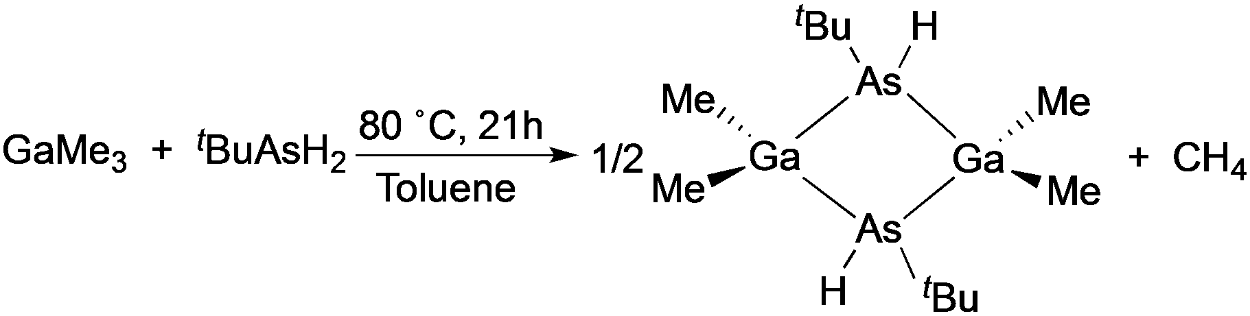
The deposition of high quality polycrystalline GaAs thin films on glass substrates was reported utilizing the single-source precursor, [Me2GaAs(H)tBu]2.54 The precursor was synthesised from the reaction of GaMe3 and tBuAsH2 in a 1 to 1.5 ratio in toluene, as shown in eqn (2). A slight excess of the arsine precursor was necessary to ensure the reaction went to completion. Polycrystalline thin films of GaAs were deposited from [Me2GaAs(H)tBu]2 in toluene via AACVD at 550 °C. Powder XRD indicated that cubic polycrystalline GaAs films had been deposited. The GaAs films were shown by EDAX mapping, X-ray photoelectron spectroscopy (XPS) depth profiling and secondary ion mass spectroscopy (SIMS) to have low incorporation of contaminants, such as carbon due to the facile β-hydride groups present in the precursor. The use of a single-source precursor in the AACVD process allowed for the deposition of films with a Ga to As ratio of 1:1 without the need for a large excess of arsenic source as typically required in dual source deposition techniques currently used for GaAs deposition. These results show the potential of AACVD as a low cost, scalable route to produce high quality thin films of GaAs from single-source precursors at atmospheric pressure.
An alternative arsenic precursor to AsH3 includes the liquid precursor, tris(dimethylaminoarsine), As(NMe2)3,44,55 which has been used in MOCVD techniques since the compound is lacking direct As–C bonds, reducing any potential carbon contamination in resulting films and it possesses a low relative decomposition temperature.64 The main decomposition products of As(NMe2)3 have been shown to include dimethylamine, hydrogen and aziridine.65 The deposition of polycrystalline GaAs thin films on glass substrates from the AACVD of a one-pot solution of the commercially available precursors, As(NMe2)3 and GaMe3, in toluene has been described.55 The resulting GaAs films were stoichiometric when a 1.5 to 1 ratio of As(NMe2)3 and GaMe3 was used in the AACVD solution. The films were relatively low in carbon and oxygen contaminations as shown by cross sectional EDA X mapping. The films were shown to have a structured morphology due to the high CVD growth rate, as shown by the SEM micrographs in Fig. 5.
 | (2) |
 | ||
| Fig. 5 SEM images of crystalline GaAs films grown via AACVD from As(NMe2)3 and GaMe3 at (a) 500 °C and (b) 550 °C. Reproduced from ref. 63 with permission from The Royal Society of Chemistry. | ||
3.3 Groups 13 and 16 (III–VI) thin films
Access to unusual or metastable phases using single-source precursors are possible either because of kinetic control of a metastable phase or because of entry into an unusual part of a phase diagram since lower deposition temperatures are often associated with the use of such precursors. Controlling the deposited phase by the molecular design of the precursor has been investigated in the CVD of gallium and indium chalcogenides.66 The III–VI compounds are semiconductors which find application in photocatalysis, optoelectronic and photovoltaic devices.67 For example, solar cells based on indium sulfide, β-In2S3, have shown a power conversion efficiency of 16.4%, comparable to the more toxic CdS based solar devices.68 They also have a potential application as passivating layers for III–V devices and are related to ternary phases, such as CuInE2 (E = S or Se) with uses in solar cells.69 Gallium sulfide can exist as a solid with several structural types and compositions. The wurtzite-type hexagonal structures, α-Ga2S3 and β-Ga2S3, as well as a monoclinic γ-Ga2S3 phase exists. The subvalent gallium sulfide (GaS) exists as a hexagonal layered structure. A range of techniques have been used to deposit III–VI thin films including solvothermal,70 spray ion layer gas reaction,71 electrostatic spray assisted vapour deposition72 and low pressure CVD.73,74 Examples of precursors to metal chalcogenides have been reviewed.75 Mixed alkyl/dithio or diselenocarbamates of gallium and indium can act as precursors to III–VI materials.76,77 Compounds of general formula [R2M(S2CNR′2)] (M = Ga: R′ = Et, R = Me, Et, CH2CMe3; R = tBu, R′ = Me, Et, nPr; M = In, R′ = Et, R = Me, Et, CH2CMe3) have been synthesised and they range from liquids (M = Ga) to low melting solids (M = In). Gallium sulfide (GaS) films have been grown by MOCVD whereas thin films of various phases of InxSy were grown by low pressure CVD.Thin films of α-Ga2S3 have been deposited by AACVD from [GaMe(SCOMe)2(dmpy)] (dmpy = 3,5-dimethylpyridine).78 The decomposition of the precursor shows two distinct steps of mass loss. The first step corresponds to the loss of dmpy and thioacetic acid and the second to the loss of acetone, as shown in Scheme 2. On heating the related compound, [Ga(SCOMe)3(dmpy)], the elimination of thioacetic anhydride was observed. At relatively low temperatures of 275–310 °C, uniform crystalline Ga2S3 films were obtained from both compounds with no evidence of impurities from carbon or oxygen. AACVD of a related mixed-metal thiocarboxylate compound, [(Ph3P)Cu(SCOPh)3In(SCOPh)] in THF at 350–450 °C resulted in the formation of β-In2S3 rather than the expected CuInS2 most likely due to dissociation of the compound in solution.79 In contrast, the Ag compound [(Ph3P)2AgIn(SCOR)4] (R = Me, Ph) did produce AgIn5S8 films via AACVD.
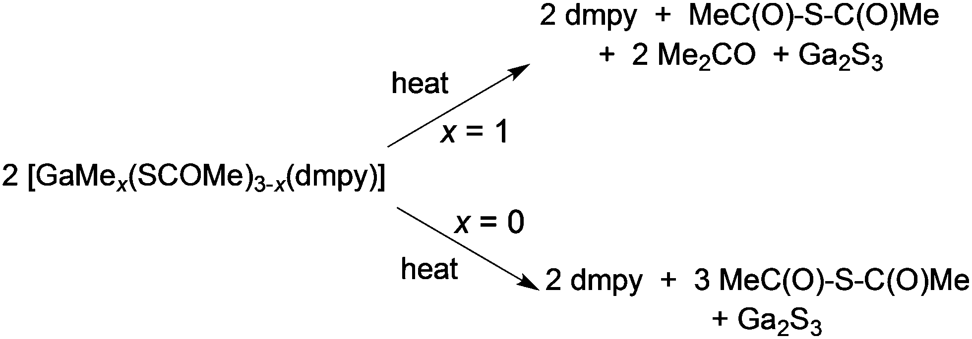 | ||
| Scheme 2 Decomposition of [GaMe(SCOMe)2(dmpy)] and [Ga(SCOMe)3(dmpy)]. | ||
An alternative class of single-source precursors based on the bidentate bis(diisopropylselenophosphoryl)amide ligand, [NH(SePiPr2)2] have been used to deposit III–VI materials.80 The compounds [R2M(SePiPr2)2N] (M = Ga, R = Me; M = In, R = Me, Et) were synthesised from the reaction of MR3 with NH(SePiPr2)2. Thin films of cubic-Ga2Se3 were grown from the gallium precursor in toluene by AACVD at 450 and 475 °C. Similarly, thin films of hexagonal γ-In2Se3 were deposited from the methyl indium derivative. The related compound [In{(SPiPr2)2N}2Cl] was shown to deposit polycrystalline tetragonal β-In2S3 films via AACVD.81
The indium and copper precursors, [In(S2PiBu2)3] and [Cu(S2PiBu2)(PPh3)2] have been synthesised via reaction of the metal chloride with sodium diisobutyldithiophosphinate and used as single-source precursors.82 The air and moisture stable indium compound [In(S2PiBu2)3] deposited thin films of cubic In2S3 on glass substrates by AACVD at 350–500 °C. Powder XRD showed that monophasic cubic In2S3 was deposited at all temperatures, as shown in Fig. 6. As expected, improved crystallinity was observed as the deposition temperature increased. When used in combination with the copper complex, thin films of CuInS2 were deposited by using a 1:1 molar ratio of [In(S2PiBu2)3] and [Cu(S2PiBu2)(PPh3)2]. The deposited In2S3 and CuInS2 thin films showed good coverage over the entire substrate and good crystallinity and hence may be suitable as a photoabsorber in solar devices. Similarly, CuInSe2, CuGaSe2 and CuIn0.7Ga0.3Se2 thin films have been deposited on glass substrates using the related [Mx(Se2PiPr2)y] precursors (M = Ga, In, Cu) at 300–350 °C.83 AACVD of the indium precursor [In(Se2PiPr2)3] at 300–500 °C in toluene yielded thin films of indium selenide in the γ-phase of In2Se3 at all temperatures. The best films were deposited at 450 °C and SEM showed uniform coverage with highly crystalline grains deposited. Different morphologies of the grains were obtained at the different deposition temperatures, as shown in Fig. 7.
 | ||
| Fig. 6 p-XRD patterns of as deposited In2S3 thin films from In[(S2PiBu2)3] precursor at temperatures (a) 350 °C, (b) 400 °C, (c) 450 °C and (d) 500 °C. Vertical lines below show the standard ICDD pattern 01-084-1385 for In2S3. Reproduced from ref. 82 with permission from the Centre National de la Recherche Scientifique (CNRS) and the Royal Society of Chemistry. | ||
 | ||
| Fig. 7 SEM images of the In2Se3 films deposited from [In(Se2PiPr2)3] at (a) 300 °C, (b) 350 °C, (c) 400 °C and (d) 450 °C. Reproduced with permission from ref. 83. Copyright 2014 Elsevier. | ||
The complexes, [Ga(μ-Te){(TePiPr2)2N}]3 and [In(μ-Te){(TePiPr2)2N}]3 were synthesised as shown in Scheme 3 and used as precursors in an AACVD process due to their low volatility.84 The gallium precursor resulted in the deposition of a mixture of cubic Ga2Te3, monoclinic GaTe and hexagonal Te at 425–475 °C. The formation of elemental tellurium is most likely to be due to decomposition of the precursor. Pure cubic In2Te3 films were deposited by AACVD of the indium precursor at 375–475 °C. The films were shown to be rough and granular by SEM, which is generally associated with the delivery of precursors as droplets and a homogeneous reaction contribution during the AACVD process.
 | ||
| Scheme 3 General synthesis of [Ga(μ-Te){N(TePiPr2)2}]3 (M = Ga, X = I) and [In(μ-Te){N(TePiPr2)2}]3 (M = In, X = Cl). | ||
Dithiocarbamate complexes have also been used as precursors to III–VI thin films in AACVD processes. Indium dithiocarbamates, of the type [In(S2CNRR′)3·n(py)] (where py = pyridine, R = R′ = Cy, n = 2; R = R′ = nPr, n = 1.5; NRR′ = Pip, n = 0.5; R = Bz, R′ = Me, n = 0)85 were synthesised by the metathetical reaction of sodium dithiocarbamate and indium trichloride in methanol/pyridine solutions, as shown in eqn (3). Typically addition of a Lewis base yields precursors with enhanced volatility, facile decomposition and sometimes air stability. For these indium complexes, the pyridine did not coordinate to the metal centre but it was present as solvate molecules in the crystal lattices of three of the compounds and the compounds were found to be air and moisture stable. AACVD using the [In(S2CNRR′)3·n(py)] precursors in toluene at 300–450 °C resulted in the deposition of tetragonal β-In2S3 thin films. The morphology of the resulting films were shown by SEM to vary with rise in substrate temperature, as shown in Fig. 8, with granular crystallites, multi-shaped interconnected crystallites and agglomerates of particles forming. UV-vis measurements of the β-In2S3 films showed band gap energies of 2.2 eV. Films deposited from [In(S2CNCy2)3]·2py were shown to be promising for application in solar cells (vide infra). Thin films of CuInS2, CuInS2, CuInSe2 and CuGaSe2 have also been grown via AACVD using the precursors [M(E2CNMenHex)3] (E = S, Se; M = Ga, In) and [Cu(E2CNMenHex)3].86
 | (3) |
 | ||
| Fig. 8 SEM images of β-In2S3 films deposited using the precursors [In(S2CNCy2)3]·2py at (a) 300 °C, (b) 350 °C and (c) 400 °C; [In(S2CN(iPr)2)3]·1.5py at (d) 300 °C, (e) 350 °C and (f) 400 °C; [In(S2CNPip)3]·0.5py at (g) 300 °C (h), 350 °C and (i) 400 °C and [In(S2CNBzMe)3] at (j) 300 °C, (k) 350 °C and (l) 400 °C. Reproduced from ref. 85 with permission from The Royal Society of Chemistry. | ||
3.4 Groups 14 and 16 (IV–VI) thin films
Tin sulfide is a IV–VI semiconductor which has three main phases: (i) SnS2, (ii) SnS and (iii) Sn2S3 which is a mixed Sn(II)/Sn(IV) compound.87 The band gaps of SnS, SnS2 and Sn2S3 are 1.3 eV, 2.18 eV and 0.95 eV respectively, and all three forms exhibit semiconducting properties. SnS has attracted a lot of attention due to its band gap, which lies between that of GaAs and silicon and depending on the tin content, SnS can be a p-type or n-type conductor. Thin films of tin(II) and tin(IV) sulfides have been investigated as semiconductors, solar collectors and photovoltaic materials. A range of methods have been used to deposit thin films of tin sulfide including spray deposition,88 chemical bath deposition,89 atomic layer deposition90 and dip deposition.91 A recent review by Lewis et al. outlines a range of methods for the deposition of thin films of binary tin chalcogenides, tin sulfide (SnS), selenide (SnSe) and telluride (SnTe), as well as describing methods to make their nanocrystalline analogues.92Tin sulfide films have been grown from single-source thiolate precursors by AACVD.93,94 The precursor, [Sn(SCH2CH2S)2] was prepared from the reaction of ethane-1,2-dithiol, 2 equiv. of nBuLi and SnCl4. AACVD of [Sn(SCH2CH2S)2] in acetone in the presence of H2S at 350–550 °C resulted in the deposition thin films of tin sulfides. The deposition temperature dictated which phase of tin sulfide was deposited; SnS2 at 350 °C, Sn2S3 at 400 °C and SnS at 500 °C and above. The use of AACVD as the deposition technique was necessary as the precursor was involatile and had poor carry over under atmospheric pressure CVD conditions. AACVD of [Sn(SCH2CH2S)2] without the use of H2S also resulted in the formation of tin sulfide films with SnS and a trace of Sn2S3 formed at 400 °C and at 500 °C and above single phase SnS. No films were deposited at 350 °C or below. AACVD of the tin monothiolate compound, [Sn(SPh)4] was shown to decompose by disulfide (RS-SR) elimination to leave reactive tin metal, which was readily oxidized to Sn3O4 in the absence of added H2S. In general, [M(SR)4] molecules have significant distortion from tetrahedral geometry due to non-covalently bonded S⋯S interactions which promotes the disulfide elimination pathway. The use of a chelating bis-thiolate in [Sn(SCH2CH2S)2] eliminates the possibility of this occurring, hence it can successfully act as a single-source precursor for tin sulfide films. AACVD of [Sn(SPh)4] with H2S added as a co-reactant did yield tin sulfide films with the film deposited at 450 °C consisting of mainly SnS2 while at 500 °C SnS was the dominant component.
Other single-source precursors that have been used in AACVD of tin sulfides include [Bz3SnCl(L)] (L = thiosemicarbazones of 4-chlorobenzaldehyde and salicylaldehyde, Bz = benzyl) in toluene at 270–370 °C to deposit SnS95,96 and a range of dithiocarbamate complexes have also been investigated.97,98 Unsymmetrical tin(II) dithiocarbamates, of the type [Sn(S2CNRR′)2] (R = Et, R′ = nBu or Et; R = Me, R′ = nBu) were synthesised either by direct reaction of the sodium salt of the dithiocarbamate with SnCl2 or via reaction of CS2 with a secondary amine in the presence of a base followed by metathesis of SnCl2. AACVD of [Sn(S2CNRR′)2] was carried out in THF at 450 and 500 °C. SnS was deposited with some contamination from SnO2 and the effect of concentration of the precursor solution was studied. The use of higher concentrations of precursors was found to be key for the formation of stoichiometric or near-to-stoichiometric films of SnS for all precursors studied, as shown in Fig. 9. A direct band gap of 1.2 eV was estimated for the films and the morphology was shown by SEM to consist of bundles of sheets comprised of small crystallites.
 | ||
| Fig. 9 The effect of concentration of precursors where (1) is [Sn(S2CNEtnBu)2], (2) is [Sn(S2CNEtnBu)2] and (3) is [Sn(S2CNEt2)2] on the stoichiometry (%Sn divided by %S found experimentally by EDAX) of SnS films deposited at 450 °C by AACVD. The dashed line indicates an ideal 1:1 Sn:S stoichiometry i.e. SnS. Reproduced with permission from ref. 98. Copyright 2014 Elsevier. | ||
A series of related organotin dithiocarbamates, [Sn(C4H9)2(S2CNRR′)2] (R = Et, R′ = Et, Me, nBu; R = Me, R′ = hexyl) were synthesised via the reaction of nBuSnCl2 with the sodium salt of the dithiocarbamate.97 The compounds, [Sn(C4H9)2(S2CNMenBu)2] and [Sn(C4H9)2(S2CNnBu2)2] were characterised by single crystal X-ray diffraction which showed that the tin has four covalent bonds (2C and 2S) in a distorted tetrahedral geometry. A weaker bonding interaction with tin along the tetrahedral face occurs from the other S atom on each dithiocarbamate ligand, as shown in Fig. 10. Therefore there are two types of Sn–S bonds, one shorter covalent Sn–S bond (∼2.526 Å) and a longer weaker Sn–S bond (∼2.940 Å). AACVD of [Sn(C4H9)2(S2CNRR′)2] (R = Et, R′ = Et, Me, nBu; R = Me, R′ = hexyl) in toluene at 400–530 °C resulted in the deposition of tin sulfide thin films. No deposition occurred at substrate temperatures below 400 °C. All the compounds primarily deposited SnS, however the presence of some SnO2 was detected by powder XRD. Hall effect measurements indicated that all the films were p-type semiconductors, which is believed to originate from high concentration of Sn vacancy sites. Band gaps varied from 1.2 to 1.7 eV for the films and the highest photosensitivity (2.1%) was obtained from deposition carried out at 500 °C using [Sn(C4H9)2(S2CNMenBu)2]. Compounds of this type have also be used to deposit thin films of Cu2(ZnyFe1−y)SnS4 (CZFTS) via AACVD in combination with Cu, Fe and Zn dithiocarbamate complexes.99
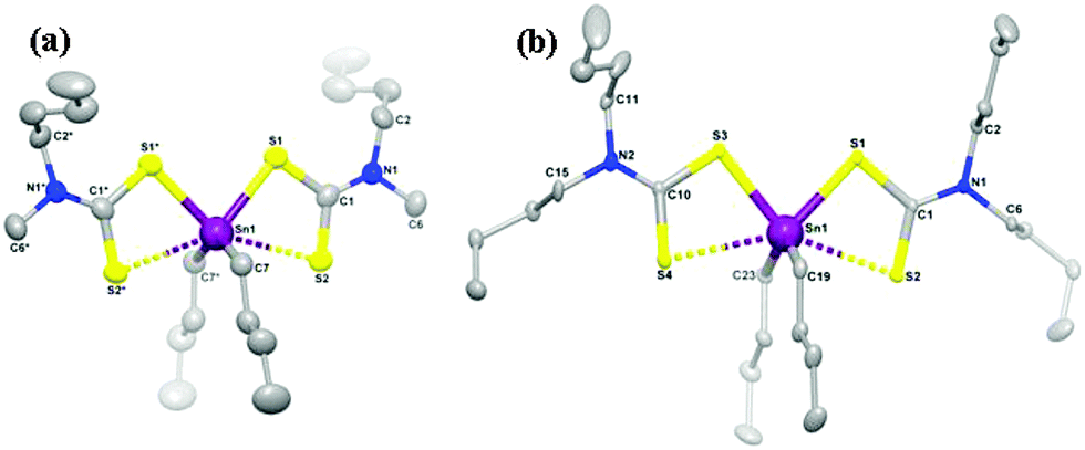 | ||
| Fig. 10 Molecular structures of (a) [Sn(C4H9)2(S2CNMenBu)2] and (b) [Sn(C4H9)2(S2CNnBu2)2] with 50% ellipsoidal probability level. All the H atoms on carbon frames are removed for clarity. Reproduced with permission from ref. 97. Copyright 2014 American Chemical Society. | ||
Thin films of SnSe have been deposited by AACVD using either [Sn(Se2PPh2)2]100 or [tBu2Sn(2-SeC5H4N)2] in THF and toluene, respectively.101 The temperature of deposition varied depending on the precursor used with SnSe films resulting from film growth at 350–400 °C from [Sn(Se2PPh2)2], whereas higher temperatures of 490–530 °C were necessary to yield SnSe films from [tBu2Sn(2-SeC5H4N)2]. When the single-source precursor, [Sn(Se2PPh2)2] was used in combination with [Cu(acac)2], copper tin selenide (Cu2SnSe3) thin films were deposited on glass substrates which could have potential applications in optoelectronics and photovoltaics.
Dithiocarbamates have also been used to deposit thin films of PbS.102,103 Lead chalcogenides are narrow band gap semiconductors with band gaps of 0.41 and 0.27 eV for PbS and PbSe, respectively and find application in high performance photoconductive infrared detectors. AACVD of the precursors [Pb(S2CNRR′)2] (R = Me, R′ = benzyl, heptyl, octadecyl; R = R′ = dioctyl or Et) in toluene at 350–525 °C on glass substrates deposited grey/black films of PbS. The morphology of the resulting films changed with deposition temperature, as shown in Fig. 11 for [Pb(S2CNMeBenzyl)2]. Deposition at higher temperatures was observed to produce thinner films with much larger and more uniform flakes of average size 8 μm. The minimum temperature required for deposition of PbS thin films from these complexes varied between 350 and 375 °C. These deposition temperatures are lower than those reported for the deposition of PbS thin films from [Pb(S2CNEtiPr)2] and [Pb(S2CNMenBu)2].94 The difference in the minimum deposition temperature seems to be related to the chain lengths of the alkyl groups on the dithiocarbamate ligand. The longer chain lengths of alkyl groups lower the deposition temperature and appeared to improve the quality of film produced resulting in more uniform and crystalline depositions.
 | ||
| Fig. 11 SEM of PbS thin films deposited from [Pb(S2CNMeBenzyl)2]. At (a) 375 °C, (b) 425 °C, (c) 475 °C and (d) 525 °C. Reproduced from ref. 102 with permission from The Royal Society of Chemistry. | ||
The lead xanthate complex, [Pb(S2COEt)2·tmeda] was used as a precursor to deposit PbS films.104 The structure of the precursor was shown by single crystal X-ray diffraction to be seven-coordinate at lead through three chelating ligands and one weak intermolecular Pb⋯S interaction, as shown in Fig. 12. AACVD of [Pb(S2COEt)2·tmeda] in THF at 200 °C resulted in the deposition of cubic PbS thin films with good surface coverage. The films were featureless, highly reflective and pinhole-free regardless of the substrate used. The deposition of PbS thin films on polyimide (Kapton) substrates by AACVD using the related compound [Pb(S2COBu)2] at temperatures as low as 150 °C has also been reported.105 The butyl xanthate was chosen as the thermal stability of the ligand was found to increase with the chain length of the alkyl substituent.
 | ||
| Fig. 12 The asymmetric unit of [Pb(S2COEt)2·tmeda] showing the labelling scheme used; thermal ellipsoids are at the 40% level. Reproduced from ref. 104 with permission from The Royal Society of Chemistry. | ||
Thin films of PbSe and PbTe have been deposited via AACVD using the precursors [Pb(4-NO2C6H4CONHCSeNiBu2)] and [Pb{(TePiPr2)2N}2] in toluene and THF/CH2Cl2, respectively.106,107 The PbSe films were grown at 250–500 °C and powder XRD showed that the cubic form of PbSe had formed at all temperatures. The films were highly textured along the (200) plane and a range of morphologies resulted which changed depending on the temperature of deposition. The morphology changed from globular crystallites to a disordered network of wires from low to high temperature. AACVD of [Pb{(TePiPr2)2N}2] below 475 °C resulted in films composed of PbTe and Te, but at 475 °C phase-pure cubic PbTe films were deposited. The surface coverage was poor and significant amounts of precursor remained in the precursor solution flask at the end of the AACVD depositions due to the poor solubility of the precursor. Films of PbTe with improved phase purity were obtained by using a hot-injection process.
3.5 Groups 15 and 16 (V–VI) thin films
Binary metal chalcogenides incorporating group 15 and 16 elements, of the type M2VE3VI (M = As, Sb, Bi; E = S, Se, Te) are an important class of semiconductors that are already used in a range of technological applications, including electronic and optoelectronic devices, thermoelectric devices and photoconducting targets. Thin films of these materials have been deposited using the solution-based techniques of spray deposition,108 spin coating,109 chemical bath deposition110 and solvothermal,111,112 as well as via low pressure MOCVD.113 However, many of these methods require complicated manipulations and equipment or have high production costs and more facile routes to fabricate V–VI thin films at low cost and in scalable ways are being investigated and a number of depositions using AACVD have been described.AACVD of the bismuth dithiocarbamate, [Bi(S2CNEt2)3]2 using a range of solvents – chloroform, dichloromethane or a 1:1 mixture of chloroform and toluene at 350–450 °C has been reported.114 The precursor was prepared from the reaction of potassium dithiocarbamate with Bi(NO3)3·5H2O in acetone. As described above, the solvent plays a significant role in determining the morphology and texture of the resulting film. In this study both polar and non-polar solvents were investigated since the polarity and specific heat capacity of the solvent are important during the decomposition process and the droplet size of the aerosol as well as the viscosity of the deposition solution can all be effected. Thin films of Bi2S3 in its orthorhombic stibnite type modification were deposited on FTO coated glass. Films deposited using dichloromethane as the solvent were found to have similar morphology to films deposited from chloroform. SEM images of films deposited from chloroform are shown in Fig. 13, which revealed that the films had complex nanostructures composed of nanotubes grown vertically on the substrate. Films grown from a mixture of chloroform and toluene (1:1) had a compact nanostructure morphology at 400 °C and a more porous structure at 450 °C, as depicted in Fig. 14. The different morphologies observed was explained by the different solvents leading to homogeneous or heterogeneous deposition reactions. During CVD decomposition of the precursor in the gas phase is termed ‘homogeneous’ whilst decomposition on the heated substrate is ‘heterogeneous’, the ratio between these two processes are directly responsible for a number of characteristics. Chloroform facilitates homogeneous reaction during deposition by evaporating and leaving the precursor molecule to vaporise in the heated zone as it is a low specific heat capacity solvent. The homogeneous reaction results in decomposition of the precursor starting in the gaseous phase, after vaporisation, which is followed by nucleation to form Bi2S3 particles. These particles can then be adsorbed onto the substrate surface and a ripening/growing process results in the formation of the nanotubes. However, with addition of toluene, a high specific heat capacity solvent, the vaporisation temperature of the aerosol droplets is increased and heterogeneous reaction is promoted. This means that the vaporised precursor and its gaseous intermediate species are adsorbed onto the surface of the heated substrate where they undergo decomposition and chemical reactions to produce the Bi2S3 thin film. The formation of porous Bi2S3 thin films at 450 °C from toluene/chloroform mixtures is due to a combination of homogeneous nucleation in the gas phase and heterogeneous growth on the substrates.
 | ||
| Fig. 13 SEM of Bi2S3 deposited via AACVD from [Bi(S2CNEt2)3]2 in chloroform at (a) 350 °C, (b) 400 °C, (c) 450 °C and (d) cross-section of film deposited at 400 °C. The inset of (b) shows a high resolution image of a nanotube. Reproduced with permission from ref. 114. Copyright 2014 American Chemical Society. | ||
 | ||
| Fig. 14 SEM of Bi2S3 thin films deposited via AACVD from [Bi(S2CNEt2)3]2 in chloroform/toluene at (a) 400 °C, (b) 450 °C, (c) and (d) show cross-section of films deposited at 400 and 450 °C, respectively. Reproduced with permission from ref. 114. Copyright 2014 American Chemical Society. | ||
The related diselenocarbamates, [Bi(Se2CNRR′)3] (R = R′ = Et, nBu, R = Me, R′ = nBu, hexyl) have been synthesised and used as precursors for the deposition of Bi2Se3 thin films.115 AACVD of [Bi(Se2CNRR′)3] in THF at 475 °C resulted in the deposition of rhombohedral Bi2Se3 films which were comprised of thin flake-like particles evenly dispersed on the glass substrates. The growth temperature was shown to affect the morphological characteristics of the film when [Bi(Se2CNMenBu)3] was used as the precursor and deposition temperatures of 450, 475 and 500 °C were investigated. The flake-like deposited particles become predominant as the growth temperature increased and SEM showed that the films were formed by an under layer of nanosized Bi2Se3 particles from which the bigger flake-like particle protrude.
Thin films of rhombohedral Bi2Se3 and orthorhombic Bi2S3 have been deposited on glass substrates from the precursors [Bi{(SePiPr2)2N}3] and [Bi{(SPR2)2N}3] (R = iPr, Ph), respectively, via AACVD.116 The films were deposited at 400–475 °C using THF as the solvent. Films were also deposited using these precursors in a low pressure MOCVD process which was found to yield higher quality films than those deposited by AACVD since no detectable phosphorus contamination was observed and the elemental composition were in better agreement with the stoichiometry expected, in contrast to AACVD films which showed some phosphorus contamination and the formation of bismuth rich films. However, a range of different morphologies were obtained using AACVD.
The related antimony telluride precursor, [Sb{(TePiPr2)2N}3], dissolved in toluene, was used to deposit pure Sb2Te3 films using the AACVD process at 375–475 °C.117 TGA indicated that the precursor decomposed by two decomposition steps. The first weight-loss corresponded to the loss of one ligand moiety, [(TePiPr2)2N], at 280 °C and the second step occurred at 325 °C resulting in weight loss suggesting formation of Sb2Te3 by further fragmentation. Therefore, the deposition studies were carried out at 325–475 °C which showed that 325 °C was too low to initiate deposition. Between 375 and 475 °C black reflective films of rhombohedral Sb2Te3 were deposited and SEM showed the formation of randomly orientated plates. Four point probe measurements of the films grown at 475 °C indicated conductivity values between 159 and 180 Ω−1 cm−1.
A number of precursors have also been used to deposit thin films of antimony sulfide in AACVD processes. Thin films of Sb2S3 have been deposited from [Sb(S2COR)3] (R = Me, Et, iPr)118 which were shown to be superior precursors compared to the related antimony dithiocarbamates, [Sb(S2CNRR′)3],119 which produced Sb2S3 films prone to oxidation. The antimony xanthate are less thermally robust than the dithiocarbamates and decomposition of [Sb(S2COR)3] was suggested to follow a metal-based variation on the Chugaev elimination, as shown in Scheme 4, where xanthates (MS2COR) are converted to alkene (RH), OCS and MSH. Powder XRD of the resulting films showed the formation of orthorhombic stibnite Sb2S3 with a minor component of Sb10S15, a monoclinic variant of Sb2S3. The morphology of the resulting films was shown to change depending on the precursor used.
 | ||
| Scheme 4 Decomposition of [Sb(S2COR)3]. | ||
Antimony thiosemicarbazones, of the type [SbCl3(L)] (L = thiosemicarbazones of thiopene-2-carboxaldehyde and cinnamaldehyde), as shown below in Fig. 15 have been used to deposit polycrystalline thin films of Sb2S3 at 320 °C in acetone.120 A rod-shaped morphology was obtained where rods of different dimensions had grown in various directions. The optical band gap for the films was found to be 3.48 eV. Thin films of antimony selenide and bismuth selenide have been grown using 2-pyridyl selenolates, of the type [M{Se-C5H3(Me-3)N}3] (M = Sb, Bi), in an AACVD process.121 The structure of the bismuth precursor is shown in Fig. 16. Bismuth selenide films, corresponding to rhombohedral Bi3Se4, hexagonal Bi3Se3, hexagonal BiSe were obtained from the bismuth compound depending on the duration and temperature of the depositions whereas Sb2Se3 was deposited using the antimony precursor.
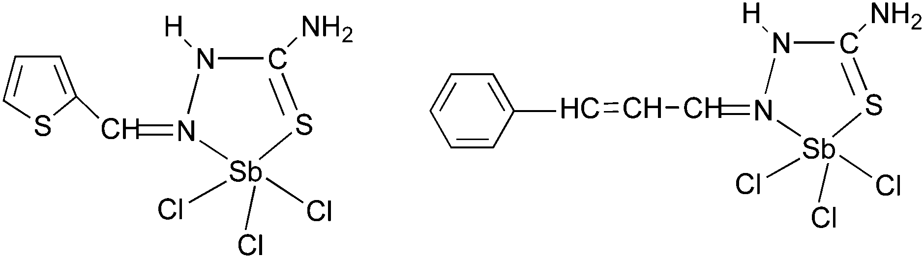 | ||
| Fig. 15 Structure of [SbCl3(L)] (L = thiosemicarbazones of thiopene-2-carboxaldehyde and cinnamaldehyde). | ||
 | ||
| Fig. 16 Crystal structure of [Bi{Se-C5H3(Me-3)N}3]·0.5H2O with atomic number scheme. Reproduced from ref. 121 with permission from The Royal Society of Chemistry. | ||
4 Main group TCOs
Section 3 described the AACVD of main group semiconductors whereas this section focuses on a particular type of semiconductor, the transparent conducting oxides (TCOs). For semiconductors to be transparent they have to absorb light at energies higher than the highest energy of visible light, which correlates to ∼3.0 eV. TCO materials must display high transparency (>80% transmittance in the visible) and high electrical conductivity. Thin film TCOs play a major role in the fabrication of a range of devices including in solar cells, optical sensors, flat panel displays and architectural glass applications and they have been used in thin film transistor (TFT) applications. The conductivity of a semiconductor is at least an order of magnitude lower than that of a metal,122 however doping is a common method to increase conductivity whilst remaining optically transparent. Better drive capacities and electrical stability are key to the improvement of TFT technologies.123,124The vast majority of TCOs are based on In2O3, SnO2, ZnO and their ternary metal oxides. These oxides exhibit n-type characteristics with electron mobility as high as 90 cm2 V−1 s−1.125 The development of p-type materials (hole transporting as opposed to the electron transporting, n-type) has been considerably slower. There have been many challenges faced in the development of materials exhibiting p-type characteristics126,127 and they are limited to materials, such as Cu2O and SnO.128
Recent research into the conductivity of n-type metal oxides has shown improvement in oxygen deficient films, leading to the belief that oxygen vacancies and metal interstitials act as electron donors.129 Theoretical and experimental work has also shown that hydrogen could play a part in n-type conductivity.130,131 However, the more traditional route of introducing impurities, or doping, is still the favoured, more controlled method to enhancing the conducting properties of the material and recent developments in the AACVD of TCOs will be described (vide infra). As devices approach their top performance, cheaper alternatives are desired, driving forward the market of inexpensive disposable electronics. Solution deposition of semiconducting main group oxides has seen much growth in the last decade from both academic and industrial research labs.129 Solution based techniques would simplify multistep synthetic procedures and lower the cost whilst still delivering a high performance. Currently there are a number of solution based techniques all with their advantages and drawbacks, including sol–gel, spray pyrolysis and dip coating.132–134 A recent review describes the AACVD of organic–inorganic nanocomposite coatings using cold plasma135 and ZnO materials and devices have also been reviewed.136
Single-source or molecular precursors can be used for the formation of thin film metal oxide materials without an additional oxygen input.137 These precursors can provide a clean and facile decomposition route that can often be more environmentally friendly, less toxic/expensive whilst at the same time eliminating the need for a mixture of precursors. Gallium oxide, indium oxide and tin oxide and their ternary oxides show excellent electrical conductivity and find application in the field of gas sensing (Section 6) and TCOs.138
4.1 Gallium and indium oxides
The β-form or monoclinic phase of gallium oxide is the most common observed, which is not usually crystalline until 900 °C, although there are reports of crystalline films grown at 600 °C,139,140 although this seems to be unusual with typical conversion occurring ∼700 °C.141 Whilst gallium oxide is amorphous at lower temperatures it shows semiconducting behaviour above 450 °C and changes in resistivity depending on the concentration of various reducing gases. Precursors to gallium oxide have received much interest and have been described in some reviews.137,142–144 Recent developments on the AACVD of gallium oxide are described below.Single-source precursors of gallium oxide can be grouped into three major classes: alkoxides, β-diketonates and β-ketoiminates (Fig. 17). Gallium alkoxide precursors that yield thin films of Ga2O3 are well reported142,145 with synthetic routes including reaction of trialkyl gallium with alcohols,139,146 reaction of GaCl3 with the salt of an alcohol147 and reaction of gallium amides with alcohols.148,149 Within the remit of ‘alkoxide’ are a number of subdivisions, including the simpler monodentate alkoxides (e.g. methoxide, ethoxide) and also donor-functionalised alkoxides which are more commonly seen as precursors in AACVD because of their ability to split oligomers into monomers via the coordination of a Lewis base.145 Whilst there are a number of variants to these donor-functionalised ligands, which improve solubility for use in AACVD and volatility for use in other types of CVD, carbon contamination is kept to a minimum with the use of shorter chains. As such it is more commonly seen that alcohols, of the type HOCH2CH2YRx (Y = O, R = Me, x = 1; Y = N, R = Me, Et, x = 2) are used in the vast majority of reported cases, with the YRx moiety acting as the Lewis base.150 The precursors were synthesized via a 1:1 reaction of GaMe3 with a donor-functionalised alcohol to yield the gallium mono-alkoxides, [Me2Ga(OCH2CH2YRx)]2.151 However, higher ratios of alcohol to trialkyl gallium resulted in the formation of mixtures of the gallium mono- and bis-alkoxides [Me3−nGa(OCH2CH2YRx)n] (n = 1, 2).152 Monomeric gallium bis-alkoxides, of the type [ClGa(OCH2CH2YRx)2] could be isolated from the reaction of GaCl3. In contrast, the addition of one equivalent of a donor-functionalised alcohol yields the dimeric gallium monoalkoxides, [Cl2Ga(OCH2CH2YRx)]2 (Fig. 18).153 A solution to this was the use of an amine elimination route, which enabled the isolation of mono-, bis- and tris-alkoxides, which have all been used to produce films of Ga2O3via AACVD.153,154
 | ||
| Fig. 17 Single-source precursors for gallium and indium oxide (M = Ga, In). | ||
 | ||
| Fig. 18 Crystal structure of: left, [Ga(OCH(CH3)CH2NMe2)2Cl], right, [Ga(OC(CH3)2CH2OMe)Cl2]2 both with thermal ellipsoids shown at the 50% probability level (hydrogen atoms omitted for clarity). Reproduced from ref. 153 with permission from the Centre National de la Recherche Scientifique (CNRS) and the Royal Society of Chemistry. | ||
The alkylgallium mono-alkoxides were initially used in low pressure CVD, however oxygen deficient thin films of gallium oxide were deposited. AACVD was then investigated due to the high solubility of the precursors in a range of solvents and in order to deposit higher purity gallium oxide.139,140 Rather than isolate and purify the dialkylgallium monoalkoxide it was generated in situ. This resulted in the AACVD reaction of GaR3 (R = Me, Et) and excess R′OH (R′ = C(CH3)2CH2OMe, CH2CH2OMe, CH2CH2NMe2, CH(CH3)CH2NMe2, CH(CH2NMe2)2) in toluene at 450 °C yielding stoichiometric Ga2O3 thin films with minimal carbon contamination. The gallium oxide films showed minimal reflectivity (5–10%) and high transmission (80–90%) with a band gap of 4.5 to 4.7 eV. Excess alcohol was used to reduce the oxygen deficiency of the films. The films deposited using GaEt3 were transparent, whereas those from GaMe3 were brown, which suggests a higher incorporation of carbon in the latter. The lower carbon observed when using the ethyl-derivative is most likely due to a facile β-hydride elimination being available for this ligand (but not the methyl).
Thin films of Ga2O3 have also been deposited by AACVD from the reaction of [Ga(NMe2)3]2 with a range of donor-functionalised alcohols, ROH (R = CH2CH2NMe2, CH(CH2NMe2)2, CH(CH3)CH2NMe2, CH2CH2OMe and C(CH3)2CH2OMe).145 The films were deposited at 550 °C from toluene solutions and simply changing the donor-functionalised alcohol yielded differing morphologies. As shown in Fig. 19, a spherical morphology resulted from the use of HOCH(CH2NMe2)2 with [Ga(NMe2)3]2, whereas fractals resulted from HOCH(CH3)CH2NMe2.
 | ||
| Fig. 19 SEM images of Ga2O3 deposited at 550 °C from [Ga(NMe2)3]2 with (a) HOCH(CH2NMe2)2 and (b) HOCH(CH3)CH2NMe in toluene. Reproduced from ref. 154 with permission from The Royal Society of Chemistry. | ||
We have also used donor-functionalised groups to stabilize gallium hydride species, of the type [{GaH2(L1)}2] and [{GaH(L2)}2] (where Lx = {Me3−xN(CH2CH2O)x} and x = 1, 2) that are stable and isolable at room temperature, as shown in Fig. 20.155 The gallium tris(alkoxide)complex [Ga(L1)3] and the related dimeric complex [{GaMe(L2)}2], have also been used as single-source precursors for the deposition of Ga2O3via AACVD with toluene as solvent. The resulting films were mostly transparent, indicating low levels of carbon contamination, and they were also mainly amorphous. The hydride compounds, [{GaH2(L1)}2] and [{GaH(L2)}2], both afforded gallium-containing films, but the best film was deposited using homoleptic [Ga(L1)3], which formed crystalline material, underneath microscale wires, at a substrate temperature of 450 °C.
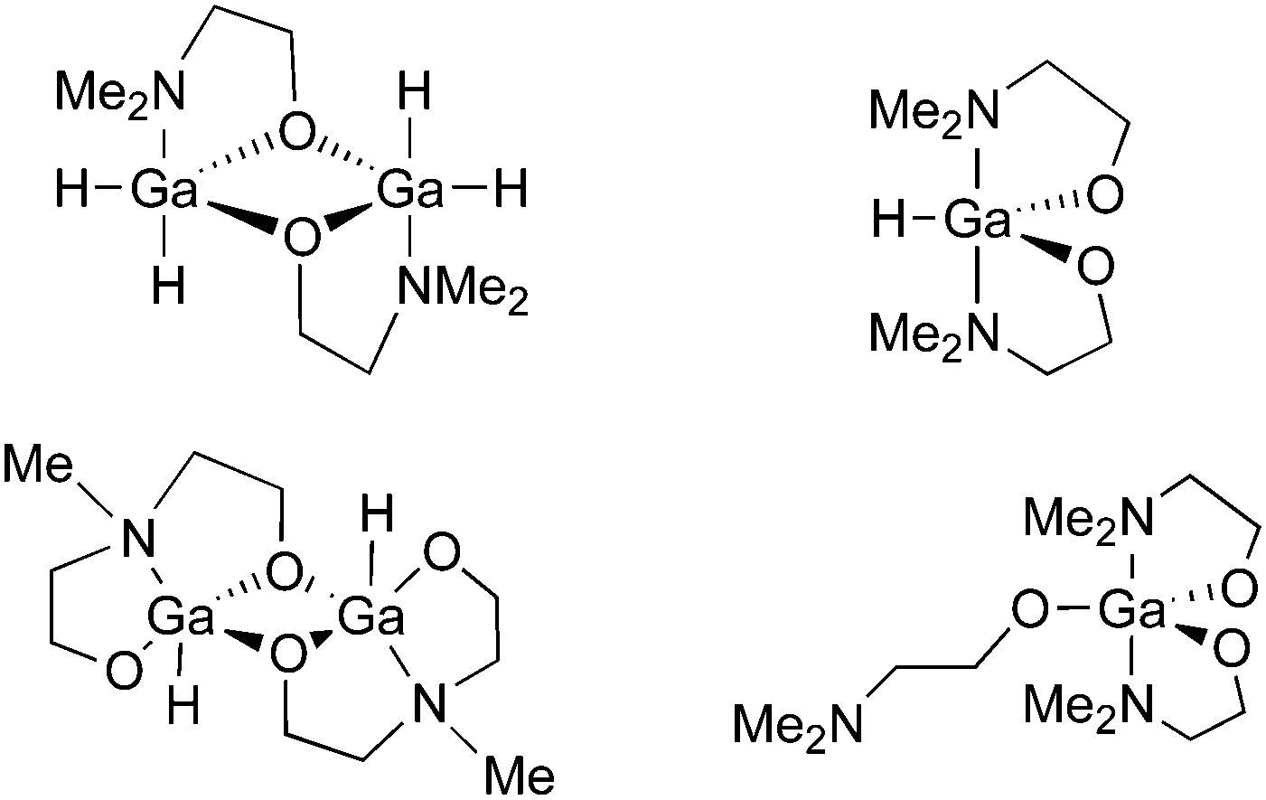 | ||
| Fig. 20 Structural diagrams of [{GaH2(L1)}2] and [{GaH(L2)}2] (where L = {Me3−xN(CH2CH2O)x} and x = 1, 2) and [Ga(L1)3]. | ||
As far back as 20 years ago commercially available ‘simple’ β-diketonates, such as [Ga(acac)3], have been used to grow films of Ga2O3 with limited success and high carbon contamination was observed in the resulting films.156–158 Accessible through facile synthetic routes,159–161 gallium tris(β-diketonates) form air stable six coordinate octahedral species, of the type [Ga(O2{R})3] (O2{R} = β-diketonate ligand). Recently, the use of these precursors for the deposition of spinel materials via AACVD has been reported.162,163 However, attempts to synthesise compounds of the type [GaX(O2{R})2] (X = Cl, Me, H) for use in CVD failed and this further evidenced the thermodynamic stability of the homoleptic tris(β-diketonates) which formed instead.164 Despite excellent solubility, the stability of gallium β-diketonates has meant that they are not ideal precursors for use in AACVD.
Gallium β-ketoiminate compounds are a more recent addition to the library of gallium precursors that currently exist. β-Ketoiminate ligands, when compared to bidentate ligands such as donor functionalised alcohols, have the advantage in that they can be easily tailored to be bi- or tetra dentate. The added functionality of groups attached to the nitrogen moiety in β-ketoimine ligands enables fine tuning of the precursor, in comparison to alkoxides and β-diketonates. The β-ketoiminate compounds contain a direct M–O bond within a delocalised ring including O and N donor atoms (Fig. 17), allowing more steric bulk to be brought into the coordination sphere of the metal centre, which can prevent oligomerisation improving precursor volatility and solubility. Furthermore, varying the R group on the N donor atom can not only increase the steric demand of the ligand, but also, with use of a polyether for example, yield multidentate ligands.142 AACVD of the β-ketoiminate gallium hydride compounds, [GaH(L3)] and [GaH2(L4)] (L3 = (CH2)2{NC(Me)CHC(Me)O}2; L4 = Me2N(CH2)3NC(Me)CHC(Me)O) in toluene at 450 °C deposited thin films of Ga2O3.165 Superior films were deposited using [GaH(L3)] (Fig. 17c and d, X = H) in comparison to [GaH2(L4)] resulting in transparent adherent films. These precursors also highlighted the advantages of AACVD as low pressure CVD was unsuccessful owing to the rapid decomposition of the precursors. However, solutions of the precursors were easily transported in an aerosol mist and deposited onto quartz substrates. Annealing the films at 1000 °C afforded crystalline films of Ga2O3. This work was particularly significant because it showed that compounds of this type could produce films with high transparency (80–90% in the visible) and low carbon contamination (<5%), significantly less than the brown films typically deposited via dialkylalkoxogallanes.139,151,154,166,167
More recently, the effect of changing the β-ketoiminate ligand on the geometry and stability of gallium and aluminium precursors was studied.168 The synthesis and crystal structures of [Ga(MeCN{iPr}–CHC(Me)O)2Cl] in a trigonal bipyramidal geometry and [Ga((CH2)2{NC(Me)–CHC(C6H5)O}2)Me] in a square based pyramid were reported and their AACVD described (Fig. 21). Both compounds produced thin films of Ga2O3 on glass at 450 °C with toluene as the solvent. In addition to gallium alkoxides and β-ketoiminates, gallium siloxide compounds, of the type [Me2Ga(OR)]2 (SiEt3, Si(OtBu)3),169 have been reported and their thermal degradation to Ga2O3 was proven via TGA.
 | ||
| Fig. 21 ORTEP diagrams showing [Ga((Me)CN(H){iPr}–CHC(Me)O)2Cl], left and [Ga((CH2)2{N(H)C(Me)–CHC(C6H5)O}2)Me], right. Thermal ellipsoids are drawn at 50% probability. Reproduced from ref. 168 with permission from the Centre National de la Recherche Scientifique (CNRS) and the Royal Society of Chemistry. | ||
 | ||
| Fig. 22 Structures of dimethylindium alkoxides. | ||
Unlike the lighter members of group 13 the oxide of indium is cubic and crystalline at 300 °C, and no phase change is observed even under AACVD conditions of 600 °C. As a material, the oxide is used in a range of devices from solar cells to gas sensors, however routes to thin film deposition has posed a problem, largely due to the lack of suitable precursors. With a view to this there has been much work in the last decade on the synthesis of indium precursors that are soluble so that they can be used in the AACVD of In2O3 and a comprehensive review of indium precursors has been published.142
In a similar manner to the gallium oxide precursors, indium oxide precursors can be grouped into two categories, namely alkoxides (Fig. 22) and β-diketonates until recently, however a range of β-ketoiminate precursors have now been reported. Literature routes to alkoxide compounds of indium often result in the formation of indium oxo alkoxo-clusters rather than isolated homoleptic alkoxides.170 This may go some way towards explaining why the availability of volatile indium alkoxide precursors is limited. Bis- or tris-alkoxides of indium cannot be synthesised from reaction of InMe3 and alcohols (mono- or donor-functionalised)171 and so amine elimination routes must be used, with [In(N(SiMe3)2)3] being a typical starting material.172 Whilst this can yield homoleptic complexes, attempts to synthesise heteroleptic indium alkoxides were unsuccessful and instead the silylamide group of the ligand was observed to migrate, resulting in the formation of dimeric species.173
Solution based studies have shown that the reaction of InMe3 and donor-functionalised alcohols form in situ compounds of the type [Me2In(OR)]2 (R = donor-functionalised ligand).171,174 As with gallium, this reaction of an alkyl indium species with a donor-functionalised alcohol (ROH, e.g. R = CH2CH2NMe2, CH2CH2OMe) can be carried out in situ in the AACVD process, which removes the additional isolation step required in many techniques. These reactions in toluene solution can be made into an aerosol using an ultrasonic humidifier and used in AACVD to deposit thin films of In2O3 (Fig. 23). The films were deposited at 550 °C, of varying thickness indicated by the clearly visible interference fringes shown on the glass.171 The films were characterised fully and shown to displayed minimal reflectivity (5–10%) and high transmission (80–90%). Owing to the porosity of the films they were shown to be hydrophilic, with water contact angles of 28°. The success of this work highlighted not just the energy cost but also the time efficiency of in situ AACVD, and the methodology has since been applied to a number of systems. SEM of the films showed that a change in morphology was observed as the donor-functionalised alcohol was altered (Fig. 23).
 | ||
| Fig. 23 Left, SEM image of In2O3 deposited from the reaction of InMe3 and HOCH2CH2OMe at 550 °C, and right, X-ray structure of [Me2In(OCH(CH2NMe2)2)]2 with thermal ellipsoids shown at the 50% probability level. Reproduced with permission from ref. 171. Copyright 2012 American Chemical Society. | ||
Indium β-diketonate precursors, much like their gallium analogues are thermodynamically stable and sublimation of [In(acac)3] is not observed until almost 200 °C.175 As with the equivalent synthetic routes employed with gallium, attempts to isolate heteroleptic indium β-diketonates failed, with only the tris(β-diketonate) isolated.164
It has been recently reported that the morphology of a film can be significantly altered by changing the solvent and/or temperature used in the AACVD process.176 Thin films of In2O3 were deposited at 350–500 °C on glass from InMe3 in methanol resulting in n-type conductivity with a resistivity of 8.60 × 10⁻⁵ Ω cm and a charge carrier concentration of 9.30 × 1020 cm−3 with mobility of the charge carriers reported to be 77.0 cm2 V−1 s−1. For comparison, films of In2O3 were also deposited via AACVD from mixtures of InMe3 and the donor functionalised alcohol, HOCH2CH2NMe2 in methanol, which resulted in resistivity of 3.66 × 10⁻⁵ Ω cm and a charge carrier concentration of 2.12 × 1020 cm−3 with mobility of the charge carriers reported to be 79.9 cm2 V−1 s−1. Overall the presence of the donor-functionalised alcohol did improve the coverage and conductivity with the sheet resistance reported to be 4.88 Ω sq−1 compared with 3.44 Ω sq−1 for the InMe3/methanol system. SEM was used to compare the resultant morphologies of the films deposited. In2O3 deposited below 400 °C from InMe3 and methanol were flat and featureless, however increasing the deposition temperature to 450 °C, resulted in the formation of agglomerated clusters, as shown in Fig. 24. The addition of the donor-functionalised alcohol gives a completely different morphology and the variation in film morphology was shown to be the result of changes in both temperature and the use of methanol.
 | ||
| Fig. 24 SEM of films grown from AACVD deposition of InMe3 and MeOH at (a) 400 °C; (b) 450 °C; and (c) 500 °C. Reproduced with permission from ref. 176 Copyright 2013 Royal Australian Chemical Institute. | ||
Indium siloxide precursors of the type [Me2In(OR)] (R = SiEt3, OSi(OtBu)3),169 have been synthesised and TGA analysis showed the former to thermally degrade to In2O3, whilst the latter formed the silicate. More recent work from the same group has reported the synthesis of novel indium(III)-tin(II) alkoxides, which under thermal treatment yielded amorphous tin-rich ITO and crystalline ITO with traces of SnO2.177
4.2 Ternary main group TCOs
Currently indium tin oxide (ITO) is the industrial standard and is used in most TCO materials. The availability of indium and therefore price still remains a concern and alternatives are actively being investigated. Gallium doped indium oxide, In2O3:Ga and fluorine doped tin oxide, SnO2:F are two viable options and whilst these materials have been deposited by a range of techniques,178–180 the following section will give an overview of the recent developments in AACVD.Gallium doped indium oxide [GaxIn2−xO3] has been shown to be an exceptional material for TCO applications with a transmittance that outstrips the competition.181 The material was successfully deposited for the first time via AACVD using a one pot reaction of GaMe3, InMe3 and an excess of the donor-functionalised alcohol, HOCH2CH2OMe, in toluene at a range of temperatures, with 450 °C found to be optimum.166 The films were transparent and XRD confirmed a homogenously Ga substituted cubic In2O3 structure. There has been much interest in the synthesis of the best performing gallium doped indium oxide, not least for its improved transmission in the blue green.166,181 The material has been studied using a novel combinatorial AACVD (cAACVD) methodology (Fig. 25). The set up for cAACVD has two separate inlets, which when one is loaded with dopant and the other the main precursor gives rise to the production of films with a compositional gradient. A grid system is then used to analyse the films, such that conductivity, transmission, thickness, dopant% and film morphology, can all be mapped against each other. This method, despite requiring large amounts of analysis does provide a single deposition route to the optimisation of functional materials. This technique has been applied to LPCVD in the investigation of multi metallic oxide materials;182–184 APCVD for the synthesis of titanium oxide,167 titanium oxynitride,185 doping of photocatalytic films,186 varying conductivity of vanadium oxide and oxynitride films,187 doped titania films188,189 and varying niobium doping in anatase.190
 | ||
| Fig. 25 Combinatorial AACVD: SEM images taken across the deposited film, showing the change from Ga2O3 (top left), through mixed gallium-indium-oxide (top right, bottom left) to In2O3 (bottom right). Reproduced from ref. 191 with permission from The Royal Society of Chemistry. | ||
Combinatorial AACVD was used for the first time to produce films of gallium-indium-oxide which showed compositional gradient across the surface.191 Powder XRD, SEM, EDAX and UV/vis spectra were used to analyse films deposited at 400 °C which showed Ga2O3 along the gallium precursor inlet, In2O3 along the indium precursor inlet and a compositional gradient between the two (Fig. 25). This initial study showed the potential of the technique, with increasing indium content correlating to increased conductivity and changes in the band gap, consistent with previously reported band gaps of indium and gallium oxide.181 Recently, cAACVD has been used to deposit thin films of TiO2–SnO2 composite materials for photocatalytic applications.192
A very recent study described the use of AACVD to investigate the effect of doping indium oxide with molybdenum or tin.184 Films were deposited at 450 °C, on glass substrates using methanol as a solvent from the precursors, [InCl3·xH2O] and [(NH4)6Mo7O24·4H2O]. The undoped In2O3 films gave high charge carrier concentrations (1 × 1020 cm−3) and charge carrier mobilities (71 cm2 V−1 s−1). However, upon doping with Mo charge carrier concentration and charge carrier mobility both increased respectively (4 × 1020 cm−3 and 119 cm2 V−1 s−1) with no decrease in the transmittance. It was shown, using XPS, XAS and DFT calculations that Mo doping facilitated carrier mobility, in contrast to Sn doped In2O3 due to spatially separated conduction which in turn reduced the ionized impurity scattering that is observed in In2O3:Sn (Fig. 26). It can be seen in Fig. 26 that the lower of the two curves, which represents regular ionized impurity scattering is significantly smaller than the higher mobility curve, which is due to scattering factors such as ‘remote’ impurities.193
 | ||
| Fig. 26 Electron mobility and concentration for undoped, Sn-doped and Mo-doped In2O3. The numbers by the data points correspond to the mol% of Mo dopant in the solution used in the AACVD. The model curves for regular ionized impurity scattering (IIS) (red line) and for remotely screened IIS (black line). All calculations are for singly ionized Mo donor atoms. Reproduced with permission from ref. 193. Copyright 2015 American Chemical Society. | ||
Thin films of ITO have also been deposited by AACVD using either aqueous or methanol solutions of InCl3·4H2O and 5 mol% SnCl2·2H2O.194 Crystalline films of ITO were grown with a (400) preferred orientation from aqueous solutions and a (440) preferred orientation from methanol, suggesting that the dissociation process of the droplets on the glass substrate and growing film surfaces is different for aqueous versus methanol solution droplets. Transparent conductive ITO films have also been deposited at 450–550 °C from a 0.2 M solution of [In(acac)3] dissolved in acetylacetone with [Sn(acac)2Br2] added as a dopant.195 The films showed excellent properties with ρ, n, and μ measured as (1–2) × 10−4 Ω cm, (1–3) × 1021 cm−3 and (20–50) cm2 V −1 s−1, comparable to ITO films deposited via sputtering.
Nanocomposite films of ITO–Si have been successfully grown via AACVD. HRTEM showed that silicon nanocrystals were separated by 8.3 nm, with a density of 1.2 × 1012 cm−1. Films were grown from a toluene solution of tin neodecanoate and ligand stabilised silicon nanocrystals onto glass substrates heated to 300 °C. Superior films gave sheet resistance of 400 Ω square−1. UV/vis provided evidence for the incorporation of the silicon nanocrystals into the ITO and it was determined that processing temperatures greater than 300 °C result in oxidation and lead to an increase in sheet resistance.196
It is well known that doping tin oxide can improve the conductivity of the resultant TCO material, but it can also enhance other properties, such as optical transmittance or stability. ITO is the most commercially used TCO material but it is followed by fluorine doped tin oxide, SnO2:F (FTO) on which there is much information published in the literature.197 There are a small range of precursors that have been used in the deposition of these materials, including tin alkoxides198,199 and β-diketonates,200,201 however only via techniques such as spin coating or spray pyrolysis,202 traditionally tin halides and NH4F or HF are used. In addition, antimony is a popular dopant, which like F alters the electronic properties of the TCO materials produced.203,204 Commercially available precursors, such as tin chloride and antimony chloride have been used205–207 to deposit thin films via a range of techniques including sol–gel,208 thermal evaporation209 and spray pyrolysis.205,210
A recent study on the AACVD of FTO used a precursor, of the type [nBuSnClx−yFy], formed in situ by the halide exchange between n-butyltin trichloride and ammonium fluoride.211 Since isolation of the precursor was not possible, evidence for the formation included XRD identification of the NH4Cl side product and XPS of the precursor, indicating the formation of a Sn–F bond. The AACVD method lends itself to in situ precursor synthesis, with the solution being immediately used to create an aerosol mist, thus removing the need for precursor isolation. This particular example highlighted the influence carrier solvent has on the functional properties of the materials.212 Varying the solvent had a significant effect on the film microstructure and therefore the properties. The resultant films showed greater performance than industrial standards, something that has not been achieved using MOCVD techniques where solvent is not used, and therefore microstructure cannot be tuned. Owing to the significant differences observed when changing the solvent in the system, a thorough investigation into the deposition variables was conducted. Films were deposited on float glass, but a range of temperatures, solvents and carrier gases were investigated. It was shown that elevated temperatures, with air as the carrier gas and propan-2-ol as the solvent produced films with optical transparency, resistivity, charge carrier concentration and mobility better than that of the current industrial standard.213
FTO films have also been deposited by AACVD using n-butyltin trichloride in methanol with varying amounts of trifluoroacetic acid at 350–550 °C.214 The films were produced using two methods for generating the aerosol: ultrasonic generation and collision type, which produce different size distributions of droplets (0.3 μm for collision type and 45 μm for ultrasonic) leading to different film characteristics. The films produced by the two AACVD methods were compared with those deposited via atmospheric pressure CVD from n-butyltin trichloride and trifluoroacetic acid at similar temperatures. It was found that films deposited using the small aerosol droplets (0.3 μm) gave films with better figures of merit than those using larger aerosol droplets (45 μm) or deposited from the same precursor set by atmospheric pressure CVD. This was attributed to the droplets generated by collision type being significantly smaller, resulting in shorter evaporation times (Fig. 27) and complete solute precipitation. The functional properties, including carrier mobility, charge-carrier density and surface morphology were found to be highly dependent on the deposition temperature using this AACVD technique with 450 °C resulting in films with optimum properties for low-emissivity coatings including a low visible haze (1.74%), high charge-carrier mobility (25 cm2 V s−1), high transmittance across the visible (80%) and high reflectance in the IR (80% at 2500 nm). In contrast, a deposition temperature of 500 °C produced FTO films ideal for use as top electrodes in photovoltaics with a low sheet resistance (3 Ω sq−1).
 | ||
| Fig. 27 Schematic of the different deposition processes, ranging from APCVD (left) which delivers the reagent to the heated substrate via a molecular gas, ultrasonic AACVD (middle) which delivers the reagent via a large aerosol droplet (45 μm) and collision type AACVD (right) which delivers the reagent species to the heated substrate for reaction via a small aerosol droplet (0.3 μm). Reproduced with permission from ref. 214. Copyright 2011 Wiley. | ||
Further attempts to improve the properties of FTO thin films were reported recently, with the incorporation of gold nanoparticles.215 A range of materials were reported in this comprehensive study, and most interestingly layered gold nanoparticles (AuNP) on FTO films exhibited blue colouration due to the surface plasmon resonance (SPR) of the AuNPs whilst maintaining high transparency in the visible, and electrical conductivity comparable to commercially available FTO (Fig. 28). This was the first report of layered TCO synthesis via AACVD with enhanced properties via production of homogenous AuNPs, the size of which was dependant on precursor concentration, with sheet resistances between 8–10 sq−1.
 | ||
| Fig. 28 Top: Schematic of layers deposited. Bottom: SEM image of AuNPs (from 0.5 × 10⁻² mmol auric acid) deposited onto a bottom plate of FTO. Reproduced from ref. 215 with permission from The Royal Society of Chemistry. | ||
Thin films of ZnO, SnO2, and composite electrodes (ZnO/SnO2 and ZnO/SnO2/Zn2SnO4) have been deposited from precursor solutions of zinc acetate and tin(IV) chloride in methanol via AACVD.216 By changing the Zn:Sn mol% ratio in the precursor solution, single phase ZnO, SnO2, and composite ZnO/SnO2 and ZnO/SnO2/Zn2SnO4 coatings were deposited on the FTO substrates at 380 °C. Controlling the Zn:Sn ratio in the precursor solution, resulted in films with a range of different morphologies, varying from compact electrodes to nanoparticle-, nanoplate-, and nanocolumn-type structures and the bandgap could be fine-tuned between that of ZnO (∼3.31 eV) and that of SnO2 (∼3.55 eV). Other dopants for SnO2 have also been investigated, including Mg in an attempt to achieve high conductivity and transparency.217,218
The recent emergence of SnO, containing tin in its lower Sn(II) oxidation state, as a potential p-type material has generated much interest. A stannous ureid compound (Fig. 29) was synthesised by the addition of 2 equivalents of tert-butyl isocyanate to [Sn(NMe2)2]2.219 AACVD of the stannous ureid in toluene at 250–350 °C resulted in the deposition of tetragonal SnO films. Powder XRD showed that the only crystalline phase at temperatures >300 °C was tetragonal SnO with no evidence of disproportionation to Sn(O) and SnO2. Raman spectroscopy confirmed the formation of SnO at all temperatures and no evidence of SnO2 or other phases, such as Sn2O3 or Sn3O4 were observed. Some evidence of surface oxidation to Sn(IV) was observed but valence band XPS spectra showed that after argon etching of the films, Sn(II) was the prominent component with a leading valence band energy of ∼2 eV. It is thought that the production of the metastable oxide, SnO, from the stannous ureid is the result of careful molecular design of the precursor and the kinetic outcome of a sequence of elimination reactions. Thin films of SnO were also deposited using the precursor [{Sn(OSiMe3)2}2] in an AACVD process with toluene as the solvent and deposition temperatures of 450 °C.220 Powder XRD confirmed the formation of SnO (and no Sn metal), which was surprising given the higher temperatures used in these depositions. SEM of the films showed the formation of irregular cubes of width about 100 nm on a thin film.
 | ||
| Fig. 29 Structure of the stannous ureid. Reproduced from ref. 218 with permission from The Royal Society of Chemistry. | ||
5 Main group photoelectrochemical and photocatalytic materials
Harvesting solar energy is a favourable alternative to burning fossil fuels however an issue that must be addressed is that of storing the electrical energy produced. This is why solar energy is preferably converted into chemical energy with the formation of hydrogen, which can be converted to electrical energy at a later stage. Water photolysis is a renewable, non-polluting method for H2 fuel generation, however there are a number of technical challenges. Under acidic conditions solar energy is used to split water into oxygen at the anode (eqn (4)) and hydrogen at the cathode (eqn (5)). This is facilitated by the use of semiconductors that absorb at the correct wavelength that are dipped into an electrolytic solution.| H2O + 2h+ → ½O2 + 2H+ | (4) |
| 2H+ + 2e− → H2 | (5) |
5.1 Bismuth oxide based materials
Bismuth oxide (Bi2O3) exists as a number of polymorphs and as such the band gap is reported to lie within the range 2.29–3.31 eV. The low temperature α phase is stable with the other phases being metastable. It was the discovery that metastable δ-Bi2O3 had the highest oxide ion conductivity of any material,230 that made it highly useful as a electrolyte, but it was its band gap that meant it was useful as a photocatalyst for degradation of pollutant dyes231 and water splitting.232 This versatile material has also found use in gas sensors,233 UV light photocatalyst,231 ferroelectric,234 multiferroic235 and superconducting oxides.236 In comparison to some other main group elements, such as gallium, there are only a limited number of bismuth precursors available, despite the same obstacles to film deposition including precursor volatility, high deposition temperatures and carbon contamination, being faced. Key attributes to successful precursors are the inclusion of at least one Bi–O bond, to overcome the energy barrier of formation in the CVD reactor, another is the use of sterically demanding ligands such that oligomerisation does not occur, affording volatile, soluble precursors.237 In general, precursor compounds of bismuth can be grouped into 3 sections; alkoxides, β-diketonates and carboxylates. These precursors can be synthesised via a number of different routes, including alcoholysis of bismuth amides (e.g. [Bi(NMe2)3]238 or the less air-sensitive bismuth silyl amide [Bi{N(SiMe3)2}3]),239 or metathesis reaction of bismuth halides and alkoxide salts.240 Due to the poor volatility, solubility and sensitivity of bismuth alkoxides, donor functionalised bismuth compounds were synthesised and their use in LPCVD reported.241,242 To further understand the potential of bismuth alkoxides and β-diketonates as CVD precursors TGA was carried out on a range of compounds.242 There are a number of reports of the deposition of thin films of Bi2O3 in the literature by a variety of techniques,143 however this section will focus on recent developments in the AACVD of the material.Bismuth β-diketonates have attracted attention as CVD precursors due to their increased stability to moisture; recently [Bi(dbm)3]2 (dbm = dibenzoylmethane) was used as a precursor in AACVD of Bi2O3 at 460–525 °C (Fig. 30). The films were synthesised via a co-deposition in order to dope with platinum nanoparticles using [H2PtCl6·H2O] as the Pt precursor. Films were found to consist of Pt–Bi2O3, and the addition of Pt particles cause hydrogen evolution during photolysis of water, something that does not occur with Pt particles or Bi2O3 alone.243 More recently the isolation of a bismuth carbamate [Bi(O2CNiPr2)3] (Fig. 31), a tetramer in the solid-state, was used to deposit Bi2O3via AACVD. It was shown in this study that δ-Bi2O3 was initially deposited, which showed superior photocatalytic activity, and at longer deposition times a thick layer of β-Bi2O3 nanowires grew on top, which proved to be less active (Fig. 32). Films were deposited from a precursor solution in hexane, on glass at temperatures ranging from 300–450 °C from 10–40 minutes.244
 | ||
| Fig. 30 X-ray crystallographic structure of [Bi(dbm)3]2. Thermal ellipsoids set at 50% probability, phenyl rings, CH2Cl2 solvent and hydrogen atoms omitted for clarity. Reproduced with permission from ref. 243. Copyright 2012 Elsevier. | ||
 | ||
| Fig. 31 Asymmetric unit of [Bi(O2CNiPr2)3] thermal ellipsoids are at 40% probability, the co-crystallised disordered solvent, and hydrogen atoms omitted for clarity. Reproduced with permission from ref. 244. Copyright 2013 American Chemical Society. | ||
 | ||
| Fig. 32 SEM of the films grown from [Bi(O2CNiPr2)3], (a and b) at 300 °C for 40 minutes, and (c and d) at 450 °C for 40 minutes. Reproduced with permission from ref. 244. Copyright 2013 American Chemical Society. | ||
5.2 Bismuth composite materials
As discussed above, there are a broad range of applications for bismuth oxide materials, as is true for its ternary and higher oxide materials. There has been much work over the last decade in the area of precursor synthesis which includes bismuth and other metals within the same molecule, to be used as single-source precursors. We direct the reader's attention to a recent review in the area of bismuth precursor development for more detail237 and here focus on the upsurge in the last five years of AACVD in this area.Bi2S3 has a band gap of 1.7 eV with an absorption coefficient of 104–105 cm−1, making it an attractive material for PEC applications.245 AACVD of bismuth selenide films was carried using at 475 °C, with the precursor, [Bi{(SePiPr2)2N}3] dissolved in THF (vide supra).108 The resulting crystalline Bi2Se3 films showed preferred orientation along the (006) direction. In the same report, [Bi{(SPR2)2N}3] (R = iPr or Ph) was used to deposit thin films of Bi2S3 at 425–475 °C, and despite poor morphology and crystallinity the band gap of the material was calculated to be 1.32 eV, in excellent agreement with the literature value of 1.3 eV. This study showed that AACVD was an excellent tool to control phase and morphology of the material (Fig. 33).116 AACVD was used again to deposit nanoparticles and tubes of Bi2S3 onto FTO coated glass. By varying the solvent used the surface morphology could be controlled; precursor solutions of [Bi(S2CNEt2)3]2 in chloroform or dichloromethane yielded films of well defined nanotubes (diameter ∼ 40 nm). Alternatively films deposited from chloroform/toluene mixtures gave compacted nanostructured morphology. Films were deposited at temperatures between 350–450 °C, and the band gap of the materials was calculated to be 1.85 and 1.8 eV respectively. PEC testing showed an excellent response, with photocurrent densities of 1.9 mA cm−2 and 1.0 mA cm−2 at 0.23 V versus Ag|AgCl|3 M|KCl, respectively.114
 | ||
| Fig. 33 SEM images of Bi2Se3 deposited from [Bi(N{SePiPr2}2)]3 by AACVD at 475 °C on glass. Reproduced with permission from ref. 116. Copyright 2004 Copyright 2013 American Chemical Society. | ||
 | ||
| Fig. 34 X-ray diffraction pattern of the as-deposited (black) and post-annealed (red) Bi2Ti2O7 thin film. Reproduced with permission from ref. 247. Copyright 2014 Elsevier. | ||
Thin films of BiFeO3 were synthesised via AACVD for the first time using the known heterometallic precursor [CpFe(CO)2BiCl2].246 Films were deposited on glass from a precursor solution in THF at 300 °C, resulting in dark orange adherent films. The band gap was calculated to lie between 2.0 and 2.2 eV and photocatalytic testing showed that the material was superior to TiO2 industrial standards when irradiated under UVA (365 nm) with an average O2 yield of 24.4% which represents a ten-fold increase over optimised B-doped TiO2 films.
Bismuth titanate (Bi2Ti2O7) thin films have been prepared for the first time via AACVD using bismuth nitrate pentahydrate in acetylacetone and titanium isopropoxide in methanol.247 The crystallinity of the films was improved by post annealing (Fig. 34). Films were deposited at 600 °C on FTO substrates, and then annealed at 600 °C for 12 hours in order to afford phase pure Bi2Ti2O7 photoelectrodes. The photocurrent density was reported as 1.8 μA cm−1 at 0.23 V versus Ag|AgCl, with a direct bandgap of 2.74 eV, making it potentially better than TiO2, since it absorbs a greater proportion of the solar spectrum and exhibits less recombination.247 Thin films of phase pure bismuth vanadate (BiVO4) photoelectrodes have also been prepared by AACVD on FTO glass substrates.248 Bismuth vanadate has a band gap of 2.4 eV in the monoclinic scheelite phase249 and is considered one of the most promising anodic semiconductor materials for PEC, not least because of its stability in pH neutral conditions.250 SEM images of the BiVO4 films deposited via AACVD from bismuth nitrate pentahydrate in acetyl acetonate and vanadyl acetyl acetonate in methanol at 500 °C, showed that the film were porous (Fig. 35). This porosity results in the films having a larger effective surface area and an increased electrode/electrolyte interfacial area allowing for a reduction in electron–hole recombination. Powder XRD showed that the monoclinic scheelite crystal structure of BiVO4 was adopted, which is ideal for PEC applications leading to superior PEC performance compared to other phases (Fig. 35). A Tauc plot showed the optical band gap to be 2.44 eV. The PEC properties were studied in aqueous 1 M Na2SO4 and showed a photocurrent density of 0.4 mA cm−2 and a maximum incident-photon-to-electron conversion efficiency (IPCE) of 19% at 1.23 V.
 | ||
| Fig. 35 XRD pattern of monoclinic BiVO4 (green) on FTO (red) coated glass substrate deposited via AACVD; below: SEM image of BiVO4 thin film at (a) 20000× and (b) 100000×. Reproduced with permission from ref. 248. Copyright 2012 Wiley. | ||
5.3 Other PEC materials
A selection of recently deposited PEC main group materials that utilise the AACVD technique in their fabrication are briefly summarised below.Zinc sulfide films were deposited on FTO coated glass at temperatures between 375–475 °C from solutions of the novel precursors [Zn(S2CNCy2)2(py)] (where Cy = cyclohexyl, py = pyridine) and [Zn(S2CN(CH2Ph)(Me))2(py)] in toluene (vide supra). The ZnS thin film electrode prepared showed promising properties for solar energy conversion and optoelectronic applications. Band gap energies of 3.36 and 3.40 eV were estimated respectively, with PEC studies showing that the films were photoactive under anodic bias conditions. It was shown that films deposited at lower temperatures (375 °C) consisted of cauliflower like structure, which was not present in films deposited at higher temperature (425 °C) (Fig. 36).39
 | ||
| Fig. 36 J–V plot of In2S3 films obtained from AACVD at 400 °C from [In(S2CNiPr2)3·1.5(py)]. Reproduced with permission from ref. 85. Copyright 2013 Royal Society of Chemistry. | ||
Thin films of indium sulfide were deposited via AACVD of novel compounds of the type, [In(S2CNRR′)3·n(py)].77 Films of β-In2S3 were deposited on FTO coated glass substrates at 300, 350 and 400 °C, with SEM images showing that varying temperature of deposition or ligand (R, R′ = iPr, n = 1.5, NRR′ = pip, n = 0.5, R = Bz, R′ = Me, n = 0) had an affect on the morphology of the films deposited (vide supra). The band gap of the films deposited was calculated to be ∼2.2 eV with the PEC properties yielding photocurrent densities of 1.25 and 0.65 mA cm−2 at 0.23 V versus Ag|AgCl for the In2S3 films deposited at 400 °C and 350 °C respectively (Fig. 37). This was the highest photocurrent and the films were prepared using the precursor [In(S2CNiPr2)·1.5(py)]. The higher response compared to the films deposited from the other precursors was thought to be due to the uniform structure of the multi-shaped β-In2S3 crystallites in the film and better interconnections of particles in the film.
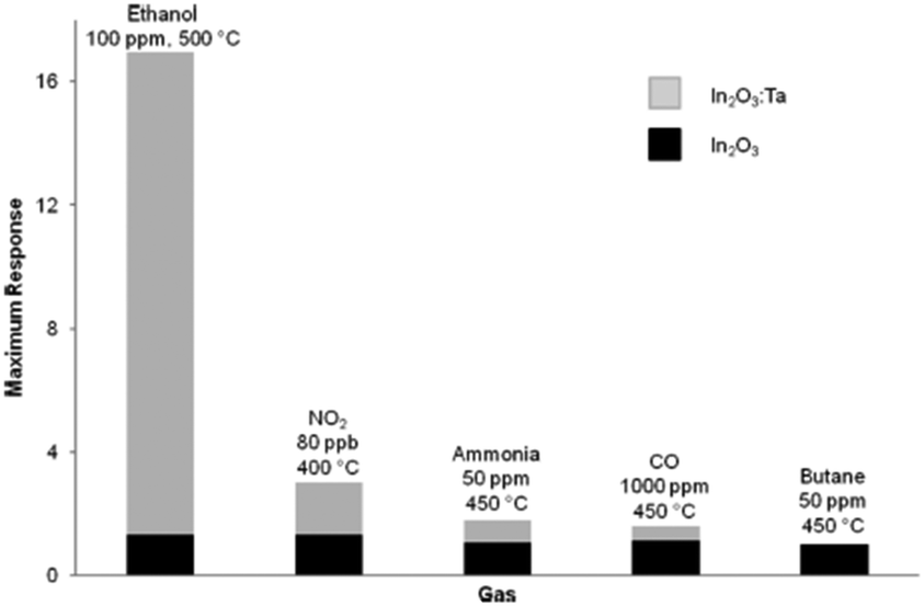 | ||
| Fig. 37 Maximum gas response of In2O3 and In2O3:Ta sensors to different gases in flowing air at optimum operating temperatures. Reproduced with permission from ref. 256. Copyright 2012 American Chemical Society. | ||
6 Main group gas sensing materials
Semiconducting metal oxides have been widely used in gas sensor devices since the absorption and desorption of a gas on the surface of a metal oxide changes the conductivity of the material.251,252 The sensitivity of the surface to a gas can be as low as parts per billion and ideally the metal oxide semiconductor sensor should have a large surface area in order to adsorb as much of the target analyte as possible on the surface to give a measurable response at such low concentrations. Gas sensor development have particularly focussed on the detection of species, such as CO2, CO, SO2, O3, NH3, NOx and H2, due to atmospheric pollution, toxicity and that they can be found at high levels in some environments. Tin dioxide is used commercially as a gas sensor. However, the search for new gas sensing materials is of great interest as SnO2 suffers from cross sensitivity issues, humidity interference and baseline drift. Main group materials that have been investigated for gas sensors applications include gallium oxide, indium oxide and tin dioxide.253 Fabrication methods need to be low cost, scalable and lead to films with appropriate morphology to achieve the required gas sensing response. Gas sensors have been widely reviewed251,252,254 including a recent review on the AACVD of some gas-sensitive nanomaterials.255 The following sections provide an up-to-date overview of main group oxide films grown by AACVD that have been investigated as gas sensors.6.1 Gallium and indium oxide based materials
Gallium oxide (Ga2O3) is an ideal material for application as a thin film gas sensor as the function of the sensor can be switched with temperature. At temperatures below 900 °C, gallium oxide thin film operates as a surface-control-type sensor to reducing gases, such as CO and ethanol. However, at temperatures above 900 °C the conductivity changes depend on the concentration of oxygen, therefore oxygen concentration can be monitored. Oxygen gas sensors have practical use in monitoring and controlling oxygen concentrations in waste gases, chemical processes and exhaust gases of automobiles. Thin films of Ga2O3 have been deposited from the in situ AACVD reaction of [Ga(NMe2)3]2 and ROH (R = CH2CH2NMe2, CH(CH2NMe2)2, CH(CH3)CH2NMe2, CH2CH2OMe and C(CH3)2CH2OMe) in toluene at 550 °C (vide supra).154 Transparent and unreflective films of gallium oxide were deposited from the reaction which generated gallium tris(alkoxides) in situ. The films were deposited on gas sensor substrates and an n-type response to ethanol at a range of temperatures was measured. Gas response was measured as the ratio between R (the resistance when exposed to ethanol) and R0 (the point immediately preceding the introduction of ethanol). The gas response was rapid and the level did not vary much throughout the experimental process. The greatest response to a gas concentration of 100 ppm of ethanol was R/R0 at 1.13. Screen-printed sensors showed a greater response (R/R0 = 2.12), which is likely due to the thinner films produced by AACVD and differences in film morphology. However, CVD sensors have been shown to give a maximum response to oxidizing or reducing gases at significantly lower temperature (100–250 °C) than screen-printed sensors.156Indium oxide (In2O3) is used in industrial and technological applications, such as toxic/dangerous gas detection with particular sensitivity to reducing gases, such as ethanol and ammonia and oxidising gases such as O3. Thin films of In2O3 and In2O3:M (M = Ti or Ta) have been deposited on glass substrates via AACVD at 450 °C from the in situ reaction of InMe3 and HOCH2CH2NMe2 and the addition of a transition metal alkoxide precursor (synthesised from the in situ reaction of [M(NMe2)n] (M = Ti, n = 4; M = Ta, n = 5) and HOCH2CH2NMe2) to produce the doped films, as shown in Scheme 5.256 The In2O3:M films were found to contain 6.5 and 2.3 at% of Ti and Ta, respectively. Films deposited on gas sensing substrates were tested for their sensitivity to increasing concentrations of both reducing and oxidizing gases (ethanol, carbon monoxide, ammonia, NO2). The tantalum doped indium oxide films (In2O3:Ta) showed an enhanced response, compared to In2O3, to both the reducing and oxidising gases with considerable selectivity to ethanol observed where the greatest gas response (R/R0) was 16.95 to 100 ppm ethanol (Fig. 37). The greater response is likely due to the reduced crystallite size for the In2O3:Ta films in comparison to the undoped indium oxide films resulting in a more reactive surface and an increased surface area to volume ratio.
 | ||
| Scheme 5 Deposition of In2O3 and In2O3:M via AACVD. | ||
6.2 Tin oxide based materials
Tin dioxide (SnO2) is efficiently employed in gas sensing applications and a comprehensive review has been reported recently which details the role of morphology and performance of this materials.257 Since the first commercial SnO2 gas sensor was successfully produced in 1968 this type of gas sensor has been widely used in a range of applications including the automobile industry and environmental monitoring. A number of techniques have been used to prepare SnO2 thin films such as the sol–gel route, evaporation and sputtering.242 AACVD has been used to deposit SnO2 thin films and their gas sensing response has been investigated.AACVD of [Sn(18-Cr-6)Cl4] and [SnCl4(H2O)2](18-Cr-6) in which the crown ether acts as a multidentate macrocyclic ligand which prevents premature hydrolysis, was carried out in a methanol/toluene mixture at 250–550 °C.258 The gas sensing properties of the resulting films were tested to 10 ppm NO2 in air at operating temperatures of 200, 250 and 300 °C. The precursor used was found to affect the SnO2 film produced with those obtained from [Sn(18-Cr-6)Cl4] having orientated particles of SnO2, a shorter recovery time and higher response to 10 ppm NO2 in air compared to [SnCl4(H2O)2](18-Cr-6). This is most likely a result of the different morphology of the films which possibly relates to the coordination of the Sn atoms where in [Sn(18-Cr-6)Cl4] the crown ether is directly coordinated to the tin atom whereas in [SnCl4(H2O)2](18-Cr-6) coordination with tin occurs through water molecules. The sensor response to NO2 was found to increase as the operating temperature increased.
AACVD of SnCl2·2H2O in absolute ethyl alcohol at 400 °C followed by annealing at 600 °C resulted in the formation of pure SnO2 films.259 By the addition of Cu(OAc)2 to the solution Cu-doped SnO2 films were also deposited. The films were tested to 50 ppm H2S at 25 °C. The Cu-doped SnO2 films showed a response of 85–50 ppm H2S gas and complete recovery between testing cycles at room temperature was observed. No response was observed to CO and CH4 and so some selectivity to H2S was found.
7 Conclusions
As described above, CVD is an attractive process for the fabrication of a wide range of materials, with use in a host of devices from gas sensors all the way to solar cells and window coatings. The main focus of this review has been the use of AACVD to deposit main group materials. Until recently, AACVD has been limited by ‘scalability’, despite its high mass transport rate but it is now seeing fast expansion, with the advent of scale-up projects in industrial plants. The benefits of this variant of CVD much outweigh its limitations; central to the process is its reliability on solubility rather than volatility, which vastly extends the range of precursors available, furthermore the technique lends itself to better morphological control. Films can be deposited on glass, steel, alumina, silica and on a host of other surfaces and uniform films with excellent adhesion can be achieved by this technique.AACVD has been shown to be an adaptable technique, it lends itself well to combinatorial AACVD, which provides a rapid route to investigate the effect of a dopant on the functional properties of a wide range of materials. As it is a solution-based technique, films with a range of compositions can be deposited, even if volatile precursors are not available. Recently, a new variant of AACVD, namely time resolved (tr)AACVD, has been described which allows the growth of a composite thin film to be studied over time.260 This method allowed the functional properties of the films to be tracked as a function of time. The production of representative samples at different times during the deposition sequence permitted changes in surface morphology, crystal structure and relative concentrations of atoms, to be linked to changes in functional properties. Other recent novel variants of AACVD include a seeding/overlay method using AACVD and atmospheric pressure CVD techniques respectively, which was shown very recently to be an excellent method to direct the growth and affect the morphology of highly transparent, conducting FTO films.261
In recent years particular attention has been drawn to the design of precursors and their ligands in order to improve the properties of the resultant films. Ligands were designed to facilitate cleaner decomposition to reduce contamination, and lower cost and to increase volatility and/or solubility, however air sensitivity and shelf life can be problematic. With the expanding field of flexible electronics, low temperature routes are sought and AACVD is an ideal technique to achieve low temperature depositions. AACVD has been shown to be a versatile technique, allowing for the deposition of a range of materials. For example, phase pure, methyl-ammonium lead iodide thin films on large glass substrates can be deposited using AACVD, which opens up a route to efficient scale up of hybrid perovskite film growth towards industrial application.262 AACVD has also been shown to be an excellent technique for the deposition of doped films, ternary and composite materials, for example PbO–TiO2 composite films263 and Cu2ZnSnSe4 (CZTSe) films.264 A recent review on the AACVD of organic–inorganic nanocomposite coatings, using cold plasma has been reported.135 An AACVD technique has also been used recently for the synthesis of large-area, mm-thick carpets of vertically aligned multi-wall carbon nanotubes (MWCNTs).265
The morphological control available through use of AACVD could be of key importance to applications in gas sensing, photocatalysis and PEC devices. Moreover, chalcogenide materials, for example kesteric materials, such as CZTSe, are of key interest for applications in polycrystalline photovoltaic solar cells. These materials are challenging to grow in thin film form in sufficient quality and AACVD has been shown to be a viable CVD method for their deposition. These areas are all ripe for further development and discovery.
Solution based techniques to TCO films are of key interest in order to simplify synthetic procedures and lower the cost whilst still delivering a high performance. AACVD has already been shown to be an excellent technique for the deposition of TCO films with figures of merit significantly beyond current commercial products. This is an area open for further research both within main group materials and other materials such as Nb-doped TiO2,266 for the preparation of indium-free TCOs and the development of low-temperature routes. Furthermore, with careful design of the precursor in combination with the use of AACVD, p-type TCOs can be deposited which represents another area worthy of further research.
Acknowledgements
The EPSRC are thanked for grant EP/K001515.References
- Chemical vapour deposition: precursors, processes and applications, ed. A. C. Jones and M. L. Hitchman, Royal Society of Chemistry, Cambridge, UK, 2009 Search PubMed.
- P. Marchand, I. A. Hassan, I. P. Parkin and C. J. Carmalt, Dalton Trans., 2013, 42, 9406 RSC.
- D. Bekermann, D. Barreca, A. Gasparotto and C. Maccato, CrystEngComm, 2012, 14, 6347 RSC.
- G. G. Condorelli, G. Malandrino and I. L. Fragalà, Coord. Chem. Rev., 2007, 251, 1931–1950 CrossRef CAS PubMed.
- A. Kurek, P. G. Gordon, S. Karle, A. Devi and S. T. Barry, Aust. J. Chem., 2014, 67, 989 CrossRef CAS.
- M. A. Malik, M. Afzaal and P. O'Brien, Chem. Rev., 2010, 110, 4417–4446 CrossRef CAS PubMed.
- O. Ambacher, J. Phys. D: Appl. Phys., 1998, 31, 2653–2710 CrossRef CAS.
- S. Strite, M. E. Lin and H. Morkoç, Thin Solid Films, 1993, 231, 197–210 CrossRef CAS.
- CVD of Compound Semiconductors, ed. A. C. Jones and P. O'Brien, Wiley-VCH Verlag GmbH, Weinheim, Germany, 1997, pp. 319–320 Search PubMed.
- P. O'Brien and R. Nomura, J. Mater. Chem., 1995, 5, 1761 RSC.
- H. M. Manasevit, J. Cryst. Growth, 1981, 55, 1–9 CrossRef CAS.
- D. Barreca, A. Gasparotto, C. Maragno, E. Tondello and C. Sada, Chem. Vap. Deposition, 2004, 10, 229–236 CrossRef CAS PubMed.
- D. Barreca, A. Gasparotto, C. Maragno and E. Tondello, J. Electrochem. Soc., 2004, 151, G428 CrossRef CAS PubMed.
- D. Barreca, A. Gasparotto, C. Maragno, R. Seraglia, E. Tondello, A. Venzo, V. Krishnan and H. Bertagnolli, Appl. Organomet. Chem., 2005, 19, 1002–1009 CrossRef CAS PubMed.
- D. Barreca, A. Gasparotto, C. Maragno, R. Seraglia, E. Tondello, A. Venzo, V. Krishnan and H. Bertagnolli, Appl. Organomet. Chem., 2005, 19, 59–67 CrossRef CAS PubMed.
- N. Savjani, J. R. Brent and P. O'Brien, Chem. Vap. Deposition, 2015, 21, 71–77 CrossRef CAS PubMed.
- M. A. Malik and P. O'Brien, Adv. Mater. Opt. Electron., 1994, 3, 171–175 CrossRef CAS PubMed.
- A. N. Gleizes, Chem. Vap. Deposition, 2000, 6, 155–173 CrossRef CAS.
- M. Afzaal, M. A. Malik and P. O'Brien, J. Mater. Chem., 2010, 20, 4031 RSC.
- A. Ashour, H. H. Afifi and S. A. Mahmoud, Thin Solid Films, 1994, 248, 253–256 CrossRef CAS.
- R. D. Pike, H. Cui, R. Kershaw, K. Dwight, A. Wold, T. N. Blanton, A. A. Wernberg and H. J. Gysling, Thin Solid Films, 1993, 224, 221–226 CrossRef.
- G. Malandrino, S. T. Finocchiaro, P. Rossi, P. Dapporto and I. L. Fragalà, Chem. Commun., 2005, 5681 RSC.
- B. Su and K. L. Choy, J. Mater. Chem., 2000, 10, 949–952 RSC.
- U. Gangopadhyay, K. Kim, D. Mangalaraj and J. Yi, Appl. Surf. Sci., 2004, 230, 364–370 CrossRef CAS PubMed.
- S. Kundu and L. C. Olsen, Thin Solid Films, 2005, 471, 298–303 CrossRef CAS PubMed.
- J. Lee, S. Lee, S. Cho, S. Kim, I. Y. Park and Y. D. Choi, Mater. Chem. Phys., 2003, 77, 254–260 CrossRef CAS.
- M. Nyman, M. J. Hampden-Smith and E. N. Duesler, Chem. Vap. Deposition, 1996, 2, 171–174 CrossRef CAS PubMed.
- M. Nyman, K. Jenkins, M. J. Hampden-Smith, T. T. Kodas, E. N. Duesler, A. L. Rheingold and M. L. Liable-Sands, Chem. Mater., 1998, 10, 914–921 CrossRef CAS.
- K. Ramasamy, M. A. Malik, M. Helliwell, J. Raftery and P. O'Brien, Chem. Mater., 2011, 23, 1471–1481 CrossRef CAS.
- K. Ramasamy, M. A. Malik, P. O'Brien and J. Raftery, Dalton Trans., 2010, 39, 1460–1463 RSC.
- K. Ramasamy, M. A. Malik, M. Helliwell, F. Tuna and P. O'Brien, Inorg. Chem., 2010, 49, 8495–8503 CrossRef CAS PubMed.
- K. Ramasamy, M. A. Malik, P. O'Brien and J. Raftery, Dalton Trans., 2009, 2196 RSC.
- G. Hogarth, Mini-Rev. Med. Chem., 2012, 12, 1202–1215 CrossRef CAS.
- S. Khalid, E. Ahmed, M. Azad Malik, D. J. Lewis, S. Abu Bakar, Y. Khan and P. O'Brien, New J. Chem., 2015, 39, 1013–1021 RSC.
- P. V. Subha, P. Valarmathi, N. Srinivasan, S. Thirumaran and K. Saminathan, Polyhedron, 2010, 29, 1078–1082 CrossRef CAS PubMed.
- P. A. Ajibade and D. C. Onwudiwe, J. Mol. Struct., 2013, 1034, 249–256 CrossRef CAS PubMed.
- M. A. Ehsan, H. N. Ming, M. Misran, Z. Arifin, E. R. T. Tiekink, A. P. Safwan, M. Ebadi, W. J. Basirun and M. Mazhar, Chem. Vap. Deposition, 2012, 18, 191–200 CrossRef CAS PubMed.
- X. Hou and K.-L. Choy, Chem. Vap. Deposition, 2006, 12, 583–596 CrossRef CAS PubMed.
- M. A. Ehsan, T. A. N. Peiris, K. G. U. Wijayantha, H. Khaledi, H. N. Ming, M. Misran, Z. Arifin and M. Mazhar, Thin Solid Films, 2013, 540, 1–9 CrossRef CAS PubMed.
- S. Mlowe, D. J. Lewis, M. Azad Malik, J. Raftery, E. B. Mubofu, P. O'Brien and N. Revaprasadu, New J. Chem., 2014, 38, 6073–6080 RSC.
- A. A. Memon, M. Dilshad, N. Revaprasadu, M. A. Malik, J. Raftery and J. Akhtar, Turk. J. Chem., 2015, 39, 169–178 CrossRef CAS.
- M. H. S. Wattoo, S. A. Tirmizi, A. Quddos, M. B. Khan, F. H. Wattoo, A. Wadood and A. B. Ghangro, Arabian J. Sci. Eng., 2011, 36, 565–571 CrossRef CAS.
- D. Oyetunde, M. Afzaal, M. A. Vincent, I. H. Hillier and P. O'Brien, Inorg. Chem., 2011, 50, 2052–2054 CrossRef CAS PubMed.
- S. S. Garje, J. S. Ritch, D. J. Eisler, M. Afzaal, P. O'Brien and T. Chivers, J. Mater. Chem., 2006, 16, 966–969 RSC.
- M. C. Copsey, A. Panneerselvam, M. Afzaal, T. Chivers and P. O'Brien, Dalton Trans., 2007, 1528 RSC.
- I. D. Rojas-Montoya, A. Santana-Silva, V. García-Montalvo, M.-Á. Muñoz-Hernández and M. Rivera, New J. Chem., 2014, 38, 4702–4710 RSC.
- H. M. Manasevit, Appl. Phys. Lett., 1968, 12, 156 CrossRef CAS PubMed.
- A. H. Cowley and R. A. Jones, Polyhedron, 1994, 13, 1149–1157 CrossRef CAS.
- F. Maury, Adv. Mater., 1991, 3, 542–548 CrossRef CAS PubMed.
- R. L. Wells, S. R. Aubuchon, S. S. Kher, M. S. Lube and P. S. White, Chem. Mater., 1995, 7, 793–800 CrossRef CAS.
- S. Schulz, S. Fahrenholz, A. Kuczkowski, W. Assenmacher, A. Seemayer, A. Hommes and K. Wandelt, Chem. Mater., 2005, 17, 1982–1989 CrossRef CAS.
- C. J. Carmalt and S. Basharat, Comprehensive Organometallic Chemistry III, Elsevier, 2007, pp. 1–34 Search PubMed.
- I. M. Watson, Coord. Chem. Rev., 2013, 257, 2120–2141 CrossRef CAS PubMed.
- A. A. Wernberg, D. J. Lawrence, H. J. Gysling, A. J. Filo and T. N. Blanton, J. Cryst. Growth, 1993, 131, 176–180 CrossRef CAS.
- M. Öztaş, M. Bedir, R. Kayalı and F. Aksoy, J. Mater. Sci.: Mater. Electron., 2006, 17, 841–845 CrossRef.
- A. R. Raju, K. Sardar and C. N. R. Rao, Mater. Sci. Semicond. Process., 2001, 4, 549–553 CrossRef CAS.
- M. Puchinger, T. Wagner, D. Rodewald, J. Bill, F. Aldinger and F. F. Lange, J. Cryst. Growth, 2000, 208, 153–159 CrossRef CAS.
- M. Puchinger, D. J. Kisailus, F. F. Lange and T. Wagner, J. Cryst. Growth, 2002, 245, 219–227 CrossRef CAS.
- H. Luo, Y. Lin, H. Wang, J. H. Lee, N. A. Suvorova, A. H. Mueller, A. K. Burrell, T. M. McCleskey, E. Bauer, I. O. Usov, M. E. Hawley, T. G. Holesinger and Q. Jia, Adv. Mater., 2009, 21, 193–197 CrossRef CAS PubMed.
- J. F. Janik, M. Drygaś, S. Stelmakh, E. Grzanka, B. Pałosz and R. T. Paine, Phys. Status Solidi A, 2006, 203, 1301–1306 CrossRef CAS PubMed.
- A. Iwata, J. Akedo and M. Lebedev, J. Am. Ceram. Soc., 2005, 88, 1067–1069 CrossRef CAS PubMed.
- S. Sathasivam, R. R. Arnepalli, B. Kumar, K. K. Singh, R. J. Visser, C. S. Blackman and C. J. Carmalt, Chem. Mater., 2014, 26, 4419–4424 CrossRef CAS.
- S. Sathasivam, R. R. Arnepalli, K. K. Singh, R. J. Visser, C. S. Blackman and C. J. Carmalt, RSC Adv., 2015, 5, 11812–11817 RSC.
- D. A. Bohling, C. R. Abernathy and K. F. Jensen, J. Cryst. Growth, 1994, 136, 118–126 CrossRef CAS.
- B. Q. Shi and C. W. Tu, J. Electron. Mater., 1999, 28, 43–49 CrossRef CAS.
- M. Bochmann, Chem. Vap. Deposition, 1996, 2, 85–96 CrossRef CAS PubMed.
- M. Lazell, P. O'Brien, D. J. Otway and J.-H. Park, J. Chem. Soc., Dalton Trans., 2000, 4479–4486 RSC.
- N. Naghavi, E. Chassaing, M. Bouttemy, G. Rocha, G. Renou, E. Leite, A. Etcheberry and D. Lincot, Energy Procedia, 2011, 10, 155–160 CrossRef CAS PubMed.
- CVD of Nonmetals, ed. W. S. Rees, Wiley-VCH Verlag GmbH, Weinheim, Germany, 1996 Search PubMed.
- F.-Y. Su, W.-D. Zhang, Y.-Y. Liu, R.-H. Huang and Y.-X. Yu, J. Solid State Electrochem., 2015, 19, 2321–2330 CrossRef CAS.
- S. Gledhill, R. Allison, N. Allsop, Y. Fu, E. Kanaki, R. Sáez-Araoz, M. Lux-Steiner and C.-H. Fischer, Thin Solid Films, 2011, 519, 6413–6419 CrossRef CAS PubMed.
- M. Wang, X. Hou, J. Liu, K. Choy, P. Gibson, E. Salem, D. Koutsogeorgis and W. Cranton, Phys. Status Solidi A, 2015, 212, 72–75 CrossRef CAS PubMed.
- K. George, C. H. (Kees) de Groot, C. Gurnani, A. L. Hector, R. Huang, M. Jura, W. Levason and G. Reid, Chem. Mater., 2013, 25, 1829–1836 CrossRef CAS.
- S. Suh and D. M. Hoffman, Chem. Mater., 2000, 12, 2794–2797 CrossRef CAS.
- J. J. Vittal and M. T. Ng, Acc. Chem. Res., 2006, 39, 869–877 CrossRef CAS PubMed.
- S. W. Haggata, M. A. Malik, M. Motevalli, P. O'Brien and J. C. Knowles, Chem. Mater., 1995, 7, 716–724 CrossRef CAS.
- A. Keys, S. G. Bott and A. R. Barron, Chem. Mater., 1999, 11, 3578–3587 CrossRef CAS.
- G. Shang, M. J. Hampden-Smith and E. N. Duesler, Chem. Commun., 1996, 1733 RSC.
- T. C. Deivaraj, J.-H. Park, M. Afzaal and J. J. Vittal, Chem. Mater., 2003, 15, 2383–2391 CrossRef CAS.
- J.-H. Park, M. Afzaal, M. Helliwell, M. A. Malik, P. O'Brien and J. Raftery, Chem. Mater., 2003, 15, 4205–4210 CrossRef CAS.
- M. Afzaal, D. Crouch, P. O'Brien and J.-H. Park, J. Mater. Sci.: Mater. Electron., 2003, 14, 555–557 CrossRef CAS.
- S. N. Malik, A. Q. Malik, R. F. Mehmood, G. Murtaza, Y. G. Alghamdi and M. A. Malik, New J. Chem., 2015, 39, 4047–4054 RSC.
- S. Mahboob, S. N. Malik, N. Haider, C. Q. Nguyen, M. A. Malik and P. O'Brien, J. Cryst. Growth, 2014, 394, 39–48 CrossRef CAS PubMed.
- S. S. Garje, M. C. Copsey, M. Afzaal, P. O'Brien and T. Chivers, J. Mater. Chem., 2006, 16, 4542 RSC.
- M. A. Ehsan, T. A. N. Peiris, K. G. U. Wijayantha, M. M. Olmstead, Z. Arifin, M. Mazhar, K. M. Lo and V. McKee, Dalton Trans., 2013, 42, 10919 RSC.
- J.-H. Park, M. Afzaal, M. Kemmler, P. O'Brien, D. J. Otway, J. Raftery and J. Waters, J. Mater. Chem., 2003, 13, 1942 RSC.
- J. A. Andrade-Arvizu, M. Courel-Piedrahita and O. Vigil-Galán, J. Mater. Sci.: Mater. Electron., 2015, 26, 4541–4556 CrossRef CAS.
- B. Thangaraju and P. Kaliannan, J. Phys. D: Appl. Phys., 2000, 33, 1054–1059 CrossRef CAS.
- C. Gao and H. Shen, Thin Solid Films, 2012, 520, 3523–3527 CrossRef CAS PubMed.
- P. Sinsermsuksakul, J. Heo, W. Noh, A. S. Hock and R. G. Gordon, Adv. Energy Mater., 2011, 1, 1116–1125 CrossRef CAS PubMed.
- S. C. Ray, M. K. Karanjai and D. DasGupta, Thin Solid Films, 1999, 350, 72–78 CrossRef CAS.
- D. J. Lewis, P. Kevin, O. Bakr, C. A. Muryn, M. A. Malik and P. O'Brien, Inorg. Chem. Front., 2014, 1, 577 RSC.
- I. P. Parkin, L. S. Price, T. G. Hibbert and K. C. Molloy, J. Mater. Chem., 2001, 11, 1486–1490 RSC.
- G. Barone, T. G. Hibbert, M. F. Mahon, K. C. Molloy, L. S. Price, I. P. Parkin, A. M. E. Hardy and M. N. Field, J. Mater. Chem., 2001, 11, 464–468 RSC.
- Y. S. Niwate, S. S. Garje, P. K. Giri, D. K. Goswami, A. Perumal and A. Chattopadhyay, AIP Conf. Proc., 2010, 1276, 56–61 CrossRef CAS PubMed.
- B. P. Bade, S. S. Garje, Y. S. Niwate, M. Afzaal and P. O'Brien, Chem. Vap. Deposition, 2008, 14, 292–295 CrossRef CAS PubMed.
- K. Ramasamy, V. L. Kuznetsov, K. Gopal, M. A. Malik, J. Raftery, P. P. Edwards and P. O'Brien, Chem. Mater., 2013, 25, 266–276 CrossRef CAS.
- P. Kevin, D. J. Lewis, J. Raftery, M. Azad Malik and P. O'Brien, J. Cryst. Growth, 2015, 415, 93–99 CrossRef CAS PubMed.
- P. Kevin, M. A. Malik and P. O'Brien, J. Mater. Chem. C, 2015, 3, 5733–5741 RSC.
- P. Kevin, S. N. Malik, M. A. Malik and P. O'Brien, Chem. Commun., 2014, 50, 14328–14330 RSC.
- R. K. Sharma, G. Kedarnath, A. Wadawale, C. A. Betty, B. Vishwanadh and V. K. Jain, Dalton Trans., 2012, 41, 12129 RSC.
- J. Akhtar, M. A. Malik, P. O'Brien and M. Helliwell, J. Mater. Chem., 2010, 20, 6116 RSC.
- M. Afzaal, K. Ellwood, N. L. Pickett, P. O'Brien, J. Raftery and J. Waters, J. Mater. Chem., 2004, 14, 1310 RSC.
- J. M. Clark, G. Kociok-Köhn, N. J. Harnett, M. S. Hill, R. Hill, K. C. Molloy, H. Saponia, D. Stanton and A. Sudlow, Dalton Trans., 2011, 40, 6893 RSC.
- J. Akhtar, M. Afzaal, M. A. Vincent, N. A. Burton, I. H. Hillier and P. O'Brien, Chem. Commun., 2011, 47, 1991 RSC.
- J. Akhtar, M. A. Malik, S. K. Stubbs, P. O'Brien, M. Helliwell and D. J. Binks, Eur. J. Inorg. Chem., 2011, 2984–2990 CrossRef CAS PubMed.
- J. S. Ritch, T. Chivers, K. Ahmad, M. Afzaal and P. O'Brien, Inorg. Chem., 2010, 49, 1198–1205 CrossRef CAS PubMed.
- M. Madoun, R. Baghdad, K. Chebbah, M. A. Bezzerrouk, L. Michez and N. Benramdane, Mater. Sci. Semicond. Process., 2013, 16, 2084–2090 CrossRef CAS PubMed.
- A. J. MacLachlan, F. T. F. O'Mahony, A. L. Sudlow, M. S. Hill, K. C. Molloy, J. Nelson and S. A. Haque, ChemPhysChem, 2014, 15, 1019–1023 CrossRef CAS PubMed.
- C. Gao, H. Shen, L. Sun and Z. Shen, Appl. Surf. Sci., 2011, 257, 7529–7533 CrossRef CAS PubMed.
- P. Hu, Y. Cao and B. Lu, Mater. Lett., 2013, 106, 297–300 CrossRef CAS PubMed.
- J. B. Biswal, S. S. Garje, J. Nuwad and C. G. S. Pillai, J. Solid State Chem., 2013, 204, 348–355 CrossRef CAS PubMed.
- T. J. Groshens, R. W. J. Gedridge and C. K. Lowe-Ma, Chem. Mater., 1994, 6, 727–729 CrossRef CAS.
- A. A. Tahir, M. A. Ehsan, M. Mazhar, K. G. U. Wijayantha, M. Zeller and A. D. Hunter, Chem. Mater., 2010, 22, 5084–5092 CrossRef CAS.
- O. C. Monteiro, T. Trindade, F. A. A. Paz, J. Klinowski, J. Waters and P. O'Brien, J. Mater. Chem., 2003, 13, 3006 RSC.
- J. Waters, D. Crouch, J. Raftery and P. O'Brien, Chem. Mater., 2004, 16, 3289–3298 CrossRef CAS.
- S. S. Garje, D. J. Eisler, J. S. Ritch, M. Afzaal, P. O'Brien and T. Chivers, J. Am. Chem. Soc., 2006, 128, 3120–3121 CrossRef CAS PubMed.
- J. R. Castro, K. C. Molloy, Y. Liu, C. S. Lai, Z. Dong, T. J. White and E. R. T. Tiekink, J. Mater. Chem., 2008, 18, 5399 RSC.
- J. Rodriguez-Castro, M. F. Mahon and K. C. Molloy, Chem. Vap. Deposition, 2006, 12, 601–607 CrossRef CAS PubMed.
- J. B. Biswal, N. V. Sawant and S. S. Garje, Thin Solid Films, 2010, 518, 3164–3168 CrossRef CAS PubMed.
- R. K. Sharma, G. Kedarnath, V. K. Jain, A. Wadawale, M. Nalliath, C. G. S. Pillai and B. Vishwanadh, Dalton Trans., 2010, 39, 8779 RSC.
- P. P. Edwards, A. Porch, M. O. Jones, D. V. Morgan and R. M. Perks, Dalton Trans., 2004, 2995 RSC.
- J. Y. Kwon, K. S. Son, J. S. Jung, T. S. Kim, M. K. Ryu, K. B. Park, B. W. Yoo, J. W. Kim, Y. G. Lee, K. C. Park, S. Y. Lee and J. M. Kim, IEEE Electron Device Lett., 2008, 29, 1309–1311 CrossRef CAS.
- R. A. Street, Adv. Mater., 2009, 21, 2007–2022 CrossRef CAS PubMed.
- M.-G. Kim, H. S. Kim, Y.-G. Ha, J. He, M. G. Kanatzidis, A. Facchetti and T. J. Marks, J. Am. Chem. Soc., 2010, 132, 10352–10364 CrossRef CAS PubMed.
- M. D. McCluskey and S. J. Jokela, J. Appl. Phys., 2009, 106, 071101 CrossRef PubMed.
- D. O. Scanlon and G. W. Watson, J. Mater. Chem., 2012, 22, 25236 RSC.
- A. Togo, F. Oba, I. Tanaka and K. Tatsumi, Phys. Rev. B: Condens. Matter Mater. Phys., 2006, 74, 195128, DOI:10.1103/PhysRevB.74.195128.
- S. R. Thomas, P. Pattanasattayavong and T. D. Anthopoulos, Chem. Soc. Rev., 2013, 42, 6910 RSC.
- A. Janotti and C. G. Van de Walle, Nat. Mater., 2007, 6, 44–47 CrossRef CAS PubMed.
- Y. J. Li, T. C. Kaspar, T. C. Droubay, A. G. Joly, P. Nachimuthu, Z. Zhu, V. Shutthanandan and S. A. Chambers, J. Appl. Phys., 2008, 104, 053711 CrossRef PubMed.
- S. Hwang, J. H. Lee, C. H. Woo, J. Y. Lee and H. K. Cho, Thin Solid Films, 2011, 519, 5146–5149 CrossRef CAS PubMed.
- G. Adamopoulos, A. Bashir, P. H. Wöbkenberg, D. D. C. Bradley and T. D. Anthopoulos, Appl. Phys. Lett., 2009, 95, 133507 CrossRef PubMed.
- B. N. Pal, B. M. Dhar, K. C. See and H. E. Katz, Nat. Mater., 2009, 8, 898–903 CrossRef CAS PubMed.
- F. Fanelli and F. Fracassi, Plasma Chem. Plasma Process., 2014, 34, 473–487 CrossRef CAS.
- Ü. Özgür, Y. I. Alivov, C. Liu, A. Teke, M. A. Reshchikov, S. Doğan, V. Avrutin, S.-J. Cho and H. Morkoç, J. Appl. Phys., 2005, 98, 041301 CrossRef PubMed.
- P. Marchand and C. J. Carmalt, Coord. Chem. Rev., 2013, 257, 3202–3221 CrossRef CAS PubMed.
- C. G. Granqvist, Sol. Energy Mater. Sol. Cells, 2007, 91, 1529–1598 CrossRef CAS PubMed.
- S. Basharat, W. Betchley, C. J. Carmalt, S. Barnett, D. A. Tocher and H. O. Davies, Organometallics, 2007, 26, 403–407 CrossRef CAS.
- Y. Kokubun, K. Miura, F. Endo and S. Nakagomi, Appl. Phys. Lett., 2007, 90, 031912 CrossRef PubMed.
- S. Mishra, S. Daniele, S. Petit, E. Jeanneau and M. Rolland, Dalton Trans., 2009, 2569 RSC.
- L. G. Bloor, C. J. Carmalt and D. Pugh, Coord. Chem. Rev., 2011, 255, 1293–1318 CrossRef CAS PubMed.
- D. Pugh, L. Bloor, S. Moniz and C. J. Carmalt, Comprehensive Inorganic Chemistry II, Elsevier, 2013, pp. 1021–1052 Search PubMed.
- M. Hellwig, K. Xu, D. Barreca, A. Gasparotto, M. Winter, E. Tondello, R. A. Fischer and A. Devi, Eur. J. Inorg. Chem., 2009, 1110–1117 CrossRef CAS PubMed.
- C. Carmalt and S. King, Coord. Chem. Rev., 2006, 250, 682–709 CrossRef CAS PubMed.
- C. E. Knapp, D. A. Wann, A. Bil, J. T. Schirlin, H. E. Robertson, P. F. McMillan, D. W. H. Rankin and C. J. Carmalt, Inorg. Chem., 2012, 51, 3324–3331 CrossRef CAS PubMed.
- Y. Chi, T.-Y. Chou, Y.-J. Wang, S.-F. Huang, A. J. Carty, L. Scoles, K. A. Udachin, S.-M. Peng and G.-H. Lee, Organometallics, 2004, 23, 95–103 CrossRef CAS.
- M. Valet and D. M. Hoffman, Chem. Mater., 2001, 13, 2135–2143 CrossRef CAS.
- L. Mîinea, S. Suh, S. G. Bott, J.-R. Liu, W.-K. Chu and D. M. Hoffman, J. Mater. Chem., 1999, 9, 929–935 RSC.
- C. E. Knapp, D. Pugh, P. F. McMillan, I. P. Parkin and C. J. Carmalt, Inorg. Chem., 2011, 50, 9491–9498 CrossRef CAS PubMed.
- C. E. Knapp, L. Pemberton, C. J. Carmalt, D. Pugh, P. F. McMillan, S. A. Barnett and D. A. Tocher, Main Group Chem., 2010, 31–40 CAS.
- S. Basharat, C. J. Carmalt, S. J. King, E. S. Peters and D. A. Tocher, Dalton Trans., 2004, 3475 RSC.
- S. Basharat, C. E. Knapp, C. J. Carmalt, S. A. Barnett and D. A. Tocher, New J. Chem., 2008, 32, 1513 RSC.
- S. Basharat, C. J. Carmalt, R. Binions, R. Palgrave and I. P. Parkin, Dalton Trans., 2008, 591 RSC.
- D. Pugh, L. G. Bloor, I. P. Parkin and C. J. Carmalt, Chem. – Eur. J., 2012, 18, 6079–6087 CrossRef CAS PubMed.
- R. Binions, C. J. Carmalt, I. P. Parkin, K. F. E. Pratt and G. A. Shaw, Chem. Mater., 2004, 16, 2489–2493 CrossRef CAS.
- T. Maruyama and S. Arai, Appl. Phys. Lett., 1992, 60, 322 CrossRef CAS PubMed.
- J. S. Kim, H. A. Marzouk, P. J. Reucroft, J. D. Robertson and C. E. Hamrin, Thin Solid Films, 1993, 230, 156–159 CrossRef CAS.
- Q. Peng, D. Hojo, K. J. Park and G. N. Parsons, Thin Solid Films, 2008, 516, 4997–5003 CrossRef CAS PubMed.
- B. Ballarin, G. A. Battiston, F. Benetollo, R. Gerbasi, M. Porchia, D. Favretto and P. Traldi, Inorg. Chim. Acta, 1994, 217, 71–78 CrossRef CAS.
- A. Ortiz, J. C. Alonso, E. Andrade and C. Urbiola, J. Electrochem. Soc., 2001, 148, F26 CrossRef CAS PubMed.
- C. E. Knapp, I. D. Prassides, S. Sathasivam, I. P. Parkin and C. J. Carmalt, ChemPlusChem, 2014, 79, 122–127 CrossRef CAS PubMed.
- C. E. Knapp, J. A. Manzi, A. Kafizas, I. P. Parkin and C. J. Carmalt, ChemPlusChem, 2014, 79, 1024–1029 CrossRef CAS PubMed.
- D. Pugh, L. G. Bloor, S. Sathasivam, I. P. Parkin and C. J. Carmalt, Eur. J. Inorg. Chem., 2011, 1953–1960 CrossRef CAS PubMed.
- D. Pugh, P. Marchand, I. P. Parkin and C. J. Carmalt, Inorg. Chem., 2012, 51, 6385–6395 CrossRef CAS PubMed.
- C. E. Knapp, G. Hyett, I. P. Parkin and C. J. Carmalt, Chem. Mater., 2011, 23, 1719–1726 CrossRef CAS.
- G. Hyett, M. Green and I. P. Parkin, J. Am. Chem. Soc., 2006, 128, 12147–12155 CrossRef CAS PubMed.
- C. E. Knapp, P. Marchand, C. Dyer, I. P. Parkin and C. J. Carmalt, New J. Chem., 2015, 39, 6585–6592 RSC.
- K. Samedov, Y. Aksu and M. Driess, ChemPlusChem, 2012, 77, 663–674 CrossRef CAS PubMed.
- D. C. Bradley, H. Chudzynska, D. M. Frigo, M. B. Hursthouse and M. A. Mazid, J. Chem. Soc., Chem. Commun., 1988, 1258 RSC.
- S. Basharat, C. J. Carmalt, S. A. Barnett, D. A. Tocher and H. O. Davies, Inorg. Chem., 2007, 46, 9473–9480 CrossRef CAS PubMed.
- S. Suh and D. M. Hoffman, J. Am. Chem. Soc., 2000, 122, 9396–9404 CrossRef CAS.
- M. Veith, S. Hill and V. Huch, Eur. J. Inorg. Chem., 1999, 1343–1350 CrossRef CAS.
- S. Basharat, C. J. Carmalt, R. Palgrave, S. A. Barnett, D. A. Tocher and H. O. Davies, J. Organomet. Chem., 2008, 693, 1787–1796 CrossRef CAS PubMed.
- T. Maruyama and K. Fukui, J. Appl. Phys., 1991, 70, 3848 CrossRef CAS PubMed.
- I. A. Hassan, A. Ratnasothy, D. S. Bhachu, S. Sathasivam and C. J. Carmalt, Aust. J. Chem., 2013, 66, 1274–1280 CAS.
- P. W. Menezes, A. Indra, P. Littlewood, M. Schwarze, C. Göbel, R. Schomäcker and M. Driess, ChemSusChem, 2014, 7, 2202–2211 CrossRef CAS PubMed.
- L. Kőrösi, S. Papp and I. Dékány, Thin Solid Films, 2011, 519, 3113–3118 CrossRef PubMed.
- J. Liu, A. W. Hains, L. Wang and T. J. Marks, Thin Solid Films, 2010, 518, 3694–3699 CrossRef CAS PubMed.
- M. A. Aouaj, R. Diaz, A. Belayachi, F. Rueda and M. Abd-Lefdil, Mater. Res. Bull., 2009, 44, 1458–1461 CrossRef CAS PubMed.
- A. Wang, N. L. Edleman, J. R. Babcock, T. J. Marks, M. A. Lane, P. R. Brazis and C. R. Kannewurf, J. Mater. Res., 2002, 17, 3155–3162 CrossRef CAS.
- R. C. Smith, N. Hoilien, J. Roberts, S. A. Campbell and W. L. Gladfelter, Chem. Mater., 2002, 14, 474–476 CrossRef CAS.
- L. Zhong, Z. Zhang, S. A. Campbell and W. L. Gladfelter, J. Mater. Chem., 2004, 14, 3203 RSC.
- B. Xia, F. Chen, S. A. Campbell, J. T. Roberts and W. L. Gladfelter, Chem. Vap. Deposition, 2004, 10, 195–200 CrossRef CAS PubMed.
- G. Hyett, M. A. Green and I. P. Parkin, J. Am. Chem. Soc., 2007, 129, 15541–15548 CrossRef CAS PubMed.
- A. Kafizas, D. Adriaens, A. Mills and I. P. Parkin, Phys. Chem. Chem. Phys., 2009, 11, 8367 RSC.
- A. Kafizas, G. Hyett and I. P. Parkin, J. Mater. Chem., 2009, 19, 1399 RSC.
- A. Kafizas and I. P. Parkin, J. Mater. Chem., 2010, 20, 2157 RSC.
- S. Sathasivam, A. Kafizas, S. Ponja, N. Chadwick, D. S. Bhachu, S. M. Bawaked, A. Y. Obaid, S. Al-Thabaiti, S. N. Basahel, C. J. Carmalt and I. P. Parkin, Chem. Vap. Deposition, 2014, 20, 69–79 CrossRef CAS PubMed.
- A. Kafizas, C. W. Dunnill and I. P. Parkin, J. Mater. Chem., 2010, 20, 8336 RSC.
- C. E. Knapp, A. Kafizas, I. P. Parkin and C. J. Carmalt, J. Mater. Chem., 2011, 21, 12644 RSC.
- N. Chadwick, S. Sathasivam, A. Kafizas, S. M. Bawaked, A. Y. Obaid, S. Al-Thabaiti, S. N. Basahel, I. P. Parkin and C. J. Carmalt, J. Mater. Chem. A, 2014, 2, 5108 CAS.
- D. S. Bhachu, D. O. Scanlon, G. Sankar, T. D. Veal, R. G. Egdell, G. Cibin, A. J. Dent, C. E. Knapp, C. J. Carmalt and I. P. Parkin, Chem. Mater., 2015, 27, 2788–2796 CrossRef.
- M. Takeuchi and K. Maki, Jpn. J. Appl. Phys., 2007, 46, 7852–7854 CrossRef CAS.
- A. Suzuki and K. Maki, Chem. Vap. Deposition, 2006, 12, 608–613 CrossRef CAS PubMed.
- S. O'Brien, K. Linehan, H. Doyle, A. Kingsley, C. Ashfield, B. Frank, L. Xie, K. Leifer, P. Thony, S. Perraud, M. E. Pemble and I. M. Povey, J. Sol–Gel Sci. Technol., 2015, 73, 666–672 CrossRef.
- Fluorinated materials for energy conversion, ed. T. Nakajima and H. Groult, Ms. C. Kreinz, Amsterdam, Boston, MA, 2005 Search PubMed.
- N. Hollingsworth, G. A. Horley, M. Mazhar, M. F. Mahon, K. C. Molloy, P. W. Haycock, C. P. Myers and G. W. Critchlow, Appl. Organomet. Chem., 2006, 20, 687–695 CrossRef CAS PubMed.
- N. Hollingsworth, G. Kociok-Köhn, K. C. Molloy and A. L. Sudlow, Dalton Trans., 2010, 39, 5446 RSC.
- H.-J. Cho, K.-W. Park, J.-K. Ahn, N.-J. Seong, S.-G. Yoon, W.-H. Park, S.-M. Yoon, D.-J. Park and J.-Y. Lee, J. Electrochem. Soc., 2009, 156, J215 CrossRef CAS PubMed.
- G. X. Liu, F. K. Shan, J. J. Park, W. J. Lee, G. H. Lee, I. S. Kim, B. C. Shin and S. G. Yoon, J. Electroceram., 2006, 17, 145–149 CrossRef CAS.
- H. Cachet, A. Gamard, G. Campet, B. Jousseaume and T. Toupance, Thin Solid Films, 2001, 388, 41–49 CrossRef CAS.
- K. H. Kim, S. W. Lee, D. W. Shin and C. G. Park, J. Am. Ceram. Soc., 1994, 77, 915–921 CrossRef CAS PubMed.
- R. G. Egdell, W. R. Flavell and P. Tavener, J. Sol–Gel Sci. Technol., 1984, 51, 345–354 CAS.
- E. Elangovan and K. Ramamurthi, Appl. Surf. Sci., 2005, 249, 183–196 CrossRef CAS PubMed.
- R. Buntem, P. Kraisingdecha and W. Sadee, Adv. Mater. Res., 2008, 55–57, 513–516 CrossRef CAS.
- T. Kololuoma and J. T. Rantala, Electron. Lett., 2000, 36, 172 CrossRef CAS.
- C. V. Santilli, A. P. Rizzato, S. H. Pulcinelli and A. F. Craievich, Phys. Rev. B: Condens. Matter Mater. Phys., 2007, 75, 205335, DOI:10.1103/PhysRevB.75.205335.
- E. C. P. E. Rodrigues and P. Olivi, J. Phys. Chem. Solids, 2003, 64, 1105–1112, DOI:10.1016/S0022-3697(03)00003-9.
- O. Malik, F. J. De la Hidalga-Wade and R. R. Amador, J. Mater. Res., 2015, 30, 2040–2045 CrossRef CAS.
- N. Noor and I. P. Parkin, Thin Solid Films, 2013, 532, 26–30 CrossRef CAS PubMed.
- N. Noor and I. P. Parkin, J. Mater. Chem. C, 2013, 1, 984–996 RSC.
- L. Schmidt-Mende and J. L. MacManus-Driscoll, Mater. Today, 2007, 10, 40–48 CrossRef CAS.
- D. S. Bhachu, M. R. Waugh, K. Zeissler, W. R. Branford and I. P. Parkin, Chem. – Eur. J., 2011, 17, 11613–11621 CrossRef CAS PubMed.
- C. K. T. Chew, C. Salcianu, P. Bishop, C. J. Carmalt and I. P. Parkin, J. Mater. Chem. C, 2015, 3, 1118–1125 RSC.
- R. Dharmadasa, A. A. Tahir and K. G. U. Wijayantha, J. Am. Ceram. Soc., 2011, 94, 3540–3546 CrossRef CAS PubMed.
- W. A. Farooq, S. M. Ali, J. Muhammad, S. D. Ali, M. H. Aziz, N. Rehman and M. Hussain, J. Mater. Sci.: Mater. Electron., 2013, 24, 5140–5146 CrossRef CAS.
- S. M. Ali, S. T. Hussain, S. A. Bakar, J. Muhammad and N. Ur Rehman, J. Phys.: Conf. Ser., 2013, 439, 012013 CrossRef.
- T. Wildsmith, M. S. Hill, A. L. Johnson, A. J. Kingsley and K. C. Molloy, Chem. Commun., 2013, 49, 8773 RSC.
- I. Barbul, A. L. Johnson, G. Kociok-Köhn, K. C. Molloy, C. Silvestru and A. L. Sudlow, ChemPlusChem, 2013, 78, 866–874 CrossRef CAS PubMed.
- M. Cargnello, A. Gasparotto, V. Gombac, T. Montini, D. Barreca and P. Fornasiero, Eur. J. Inorg. Chem., 2011, 4309–4323 CrossRef CAS PubMed.
- D. Barreca, G. Carraro, V. Gombac, A. Gasparotto, C. Maccato, P. Fornasiero and E. Tondello, Adv. Funct. Mater., 2011, 21, 2611–2623 CrossRef CAS PubMed.
- S. Kaneco, T. Miwa, K. Hachisuka, H. Katsumata, T. Suzuki, S. C. Verma and K. Sugihara, in Nanocatalysis for Fuels and Chemicals, ed. A. K. Dalai, American Chemical Society, Washington, DC, 2012, vol. 1092, pp. 25–36 Search PubMed.
- F. E. Osterloh, Nanoscale Effects in Water Splitting Photocatalysis, Springer Berlin Heidelberg, Berlin, Heidelberg, 2015 Search PubMed.
- S. N. Ariffin, H. N. Lim, Z. A. Talib, A. Pandikumar and N. M. Huang, Int. J. Hydrogen Energy, 2015, 40, 2115–2131 CrossRef CAS PubMed.
- M. G. Walter, E. L. Warren, J. R. McKone, S. W. Boettcher, Q. Mi, E. A. Santori and N. S. Lewis, Chem. Rev., 2010, 110, 6446–6473 CrossRef CAS PubMed.
- M. Grätzel, Nature, 2001, 414, 338–344 CrossRef PubMed.
- S. Choudhary, S. Upadhyay, P. Kumar, N. Singh, V. R. Satsangi, R. Shrivastav and S. Dass, Int. J. Hydrogen Energy, 2012, 37, 18713–18730 CrossRef CAS PubMed.
- B. Chen, S. Xiang and G. Qian, Acc. Chem. Res., 2010, 43, 1115–1124 CrossRef CAS PubMed.
- A. M. Azad, S. Larose and S. A. Akbar, J. Mater. Sci., 1994, 29, 4135–4151 CrossRef CAS.
- H. Weidong, Q. Wei, W. Xiaohong, D. Xianbo, C. Long and J. Zhaohua, Thin Solid Films, 2007, 515, 5362–5365 CrossRef PubMed.
- K. Gurunathan, Int. J. Hydrogen Energy, 2004, 29, 933–940 CrossRef CAS PubMed.
- G. Sarala Devi, S. V. Manorama and V. J. Rao, Sens. Actuators, B, 1999, 56, 98–105, DOI:10.1016/S0925-4005(99)00164-1.
- B. H. Park, B. S. Kang, S. D. Bu, T. W. Noh, J. Lee and W. Jo, Nature, 1999, 401, 682–684 CrossRef CAS.
- P.-F. Zhuang, T. Liu, X.-H. Xie, C. He and C.-Y. Duan, Dalton Trans., 2015, 44, 464–467 RSC.
- C. Michel, M. Hervieu, M. M. Borel, A. Grandin, F. Deslandes, J. Provost and B. Raveau, Z. Phys. B: Condens. Matter, 1987, 68, 421–423 CrossRef CAS.
- M. Mehring, Coord. Chem. Rev., 2007, 251, 974–1006 CrossRef CAS PubMed.
- M. A. Matchett, M. Y. Chiang and W. E. Buhro, Inorg. Chem., 1990, 29, 358–360 CrossRef CAS.
- M.-C. Massiani, R. Papiernik, L. G. Hubert-Pfalzgraf and J.-C. Daran, Polyhedron, 1991, 10, 437–445 CrossRef CAS.
- C. Knispel, C. Limberg and B. Ziemer, Inorg. Chem., 2010, 49, 4313–4318 CrossRef CAS PubMed.
- P. A. Williams, A. C. Jones, M. J. Crosbie, P. J. Wright, J. F. Bickley, A. Steiner, H. O. Davies, T. J. Leedham and G. W. Critchlow, Chem. Vap. Deposition, 2001, 7, 205 CrossRef CAS.
- S. J. A. Moniz, C. S. Blackman, C. J. Carmalt and G. Hyett, J. Mater. Chem., 2010, 20, 7881 RSC.
- S. J. A. Moniz, D. Bhachu, C. S. Blackman, A. J. Cross, S. Elouali, D. Pugh, R. Quesada Cabrera and S. Vallejos, Inorg. Chim. Acta, 2012, 380, 328–335 CrossRef CAS PubMed.
- S. D. Cosham, M. S. Hill, G. A. Horley, A. L. Johnson, L. Jordan, K. C. Molloy and D. C. Stanton, Inorg. Chem., 2014, 53, 503–511 CrossRef CAS PubMed.
- L. M. Peter, K. G. U. Wijayantha, D. J. Riley and J. P. Waggett, J. Phys. Chem. B, 2003, 107, 8378–8381 CrossRef CAS.
- S. J. A. Moniz, R. Quesada-Cabrera, C. S. Blackman, J. Tang, P. Southern, P. M. Weaver and C. J. Carmalt, J. Mater. Chem. A, 2014, 2, 2922 CAS.
- A. McInnes, J. S. Sagu and K. G. U. Wijayantha, Mater. Lett., 2014, 137, 214–217 CrossRef CAS PubMed.
- P. Brack, J. S. Sagu, T. A. N. Peiris, A. McInnes, M. Senili, K. G. U. Wijayantha, F. Marken and E. Selli, Chem. Vap. Deposition, 2015, 21, 41–45 CrossRef CAS PubMed.
- S. J. Hong, S. Lee, J. S. Jang and J. S. Lee, Energy Environ. Sci., 2011, 4, 1781 CAS.
- J. R. McKone, N. S. Lewis and H. B. Gray, Chem. Mater., 2014, 26, 407–414 CrossRef CAS.
- A. Tricoli, M. Righettoni and A. Teleki, Angew. Chem., Int. Ed., 2010, 49, 7632–7659 CrossRef CAS PubMed.
- M. M. Arafat, B. Dinan, S. A. Akbar and A. S. M. A. Haseeb, Sensors, 2012, 12, 7207–7258 CrossRef CAS PubMed.
- L. Filipovic and S. Selberherr, Sensors, 2015, 15, 7206–7227 CrossRef CAS PubMed.
- E. Comini, Sensors, 2013, 13, 10659–10673 CrossRef CAS PubMed.
- F. E. Annanouch, S. Vallejos, T. Stoycheva, C. Blackman and E. Llobet, Thin Solid Films, 2013, 548, 703–709 CrossRef CAS PubMed.
- L. G. Bloor, J. Manzi, R. Binions, I. P. Parkin, D. Pugh, A. Afonja, C. S. Blackman, S. Sathasivam and C. J. Carmalt, Chem. Mater., 2012, 24, 2864–2871 CrossRef CAS.
- S. Das and V. Jayaraman, Prog. Mater. Sci., 2014, 66, 112–255 CrossRef CAS PubMed.
- T. T. Stoycheva, S. Vallejos, R. G. Pavelko, V. S. Popov, V. G. Sevastyanov and X. Correig, Chem. Vap. Deposition, 2011, 17, 247–252 CrossRef CAS PubMed.
- J. Zhao, S. Wu, J. Liu, H. Liu, S. Gong and D. Zhou, Sens. Actuators, B, 2010, 145, 788–793 CrossRef CAS PubMed.
- N. P. Chadwick, S. Sathasivam, S. M. Bawaked, M. Mokhtar, S. A. Althabaiti, S. N. Basahel, I. P. Parkin and C. J. Carmalt, J. Mater. Chem. A, 2015, 3, 4811–4819 CAS.
- N. Noor, C. K. T. Chew, D. S. Bhachu, M. R. Waugh, C. J. Carmalt and I. P. Parkin, J. Mater. Chem. C, 2015, 3, 9359–9368, 10.1039/C5TC02144H.
- D. S. Bhachu, D. O. Scanlon, E. J. Saban, H. Bronstein, I. P. Parkin, C. J. Carmalt and R. G. Palgrave, J. Mater. Chem. A, 2015, 3, 9071–9073 CAS.
- D. S. Bhachu, S. Sathasivam, C. J. Carmalt and I. P. Parkin, Langmuir, 2014, 30, 624–630 CrossRef CAS PubMed.
- P. Kevin, S. N. Malik, M. A. Malik and P. O'Brien, Mater. Lett., 2015, 152, 60–64 CrossRef CAS PubMed.
- S. S. Meysami, A. A. Koós, F. Dillon, M. Dutta and N. Grobert, Carbon, 2015, 88, 148–156 CrossRef CAS PubMed.
- D. S. Bhachu, S. Sathasivam, G. Sankar, D. O. Scanlon, G. Cibin, C. J. Carmalt, I. P. Parkin, G. W. Watson, S. M. Bawaked, A. Y. Obaid, S. Al-Thabaiti and S. N. Basahel, Adv. Funct. Mater., 2014, 24, 5075–5085 CrossRef CAS PubMed.
| This journal is © The Royal Society of Chemistry 2016 |