
Refractometric and colorimetric index sensing by a plasmon-coupled hybrid AAO nanotemplate†
Kyuyoung Baea,
Jungmin Leea,
Gumin Kanga,
Do-Sik Yoob,
Chang-Won Lee *c and
Kyoungsik Kim*a
*c and
Kyoungsik Kim*a
aSchool of Mechanical Engineering, Yonsei University, 50 Yonsei-ro, Seodaemun-gu, Seoul 120-749, Korea. E-mail: kks@yonsei.ac.kr
bSchool of Electronic and Electrical Engineering, Hongik University, 94 Wausan-Ro, Mapo-Gu, Seoul 121-791, Republic of Korea
cSamsung Advanced Institute of Technology, Suwon, Korea. E-mail: cwlee42@gmail.com
First published on 17th November 2015
Abstract
Facile optical sensors capable of measuring a small change in an analyte’s refractive index have been highlighted as the demand for environmental and Internet-of-Things (IoT) applications increases. In this work, we demonstrate a large-area refractive index sensor capable of refractometric and colorimetric sensing with a plasmon-coupled hybrid nanotemplate of anodic aluminum oxide (AAO). The nanotemplate enhances the figure-of-merit and sensitivity due to the coupled mode of the Fabry–Perot microcavity and metallic nanosurfaces. The increased mode confinement and interaction between AAO pores and analytes show highly modulated reflection spectra, which enable a refractive index sensitivity up to 348 nm per RIU and a figure-of-merit value up to 27.7. Also, the vivid color change induced from infiltrated analytes allows a colorimetric sensing performance up to RIU/ΔE ∼ 0.006 according to CIELab 1931 analysis. The key features of our device are simultaneous applications to superb dual (refractometric and colorimetric) sensing schemes by the plasmon-coupled hybrid AAO nanotemplate.
Introduction
Late advancements in nanotechnology have prompted new applications for optical sensors that can measure a broad range of chemical or biomolecular analytes in environmental and Internet-of-Things (IoT) applications.1–10 In order to apply optical sensors to IoT applications, it is required to have a small form factor with minimal power consumption. In addition, acquired data need to be transmitted and analyzed in a simple way without external batteries. Therefore it is very feasible to use smartphones or digital cameras for optical sensing since they are already well-distributed, easy to use and have enough computational power to analyze data.The optical sensors detect the electromagnetic spectrum shift arising from the refractive index change when an analyte target approaches to an active region.11 Generally, two approaches have been available for index sensing: refractometric and colorimetric. Refractometric sensing analyses shift the transmission or reflection spectrum due to electromagnetic interaction between the active region and the target analytes. Therefore, a spectroscopic setup is necessary for capturing and analysing spectra. On the other hand, colorimetric sensing uses no external device and just uses a recognized color change. For refractometric index sensing, methods such as a polarimetric measurement,12 a resonance spectrum shift of surface plasmon of gold with molecular labeling,13,14 and a light waveguide based on anodic aluminum oxide (AAO)15–17 have been successfully demonstrated. For colorimetric index sensing, color changes of a silver nanovolcano array,18 a 1D nanotemplate based on mixed metal oxide (MMO)–TiO2,19 coupled silicon nanowire arrays20 and a gold nanopatch array21 have been measured and analysed.
Among various optical sensors, surface plasmon resonance (SPR) sensors have been intensively studied owing to their ability to enhance the local electromagnetic field at the nanoscale.22,23 SPR sensors are very sensitive to the change of the dielectric permittivity within the active region, where the interaction between the plasmonic nanostructure and the analyte takes place. The local electromagnetic mode can be detected by far-field spectroscopy through a radiative damping process.24 One of the most significant problems of the SPR-based sensor is broad plasmonic resonance due to large absorption loss of metals. The broad linewidth limits important sensing characteristics – the figure-of-merit (FOM), which is defined as the refractive index sensitivity divided by the spectral linewidth.23,25–27 Another problem of SPR-based sensors is a small spatial sensing depth of the active region, which is only constrained to a few nanometers around the plasmonic nanostructure.26,28,29 Therefore, a sophisticated micro-spectroscopic setup is required to collect the far-field efficiently and measure the spectrum.
To overcome these problems, several methods have been proposed to enhance the sensitivity, FOM, and detection scheme of SPR-based sensors. First, strong coupling of broad SPR to a system with narrow plasmonic resonance by the Fano effect30–32 or electromagnetically induced transparency33,34 have been proposed. The strongly coupled system can be introduced by the propagating mode in a periodic grating35 or coupling between individual metallic rods.24,31,35 The coupled mode shows altered plasmonic resonance spectra to more asymmetric and narrower shapes, which provides a higher FOM and sensitivity for refractive index sensing. The second method is to use the plasmonic waveguide structure.36,37 A change of the plasmonic mode due to a filled analyte in a hollow metallic cavity leads to an enhanced sensitivity and FOM. The third method is to use coupling SPR with an optical microcavity to decrease the resonance linewidth.38–41 The linewidth of such a hybrid resonance can be reduced by the modified cavity Q factor determined by radiative damping of the coupled system.
However, all these methods require a lithographic fabrication process and a sophisticated spectroscopic setup in order to obtain a high refractive index sensitivity and FOM. In this paper, we demonstrate a facile method to fabricate a large-area and low-cost template for coupling SPR and an optical Fabry–Perot microcavity. The AAO template with a deposited metal nanosurface is used not only to couple electromagnetic modes, but also to simplify the analyte infiltration scheme. The plasmon-coupled modes enhance the electromagnetic field and the interaction with the analyte at the AAO–air interface to make the Fabry–Perot mode have large Q factors. The AAO template is employed as the fabrication method is simple in spite of its nanoscale structure compared to electron beam lithography, which is commonly used for nanofabrication. Excellent chemical and mechanical stability of aluminum oxide also led to the AAO template being applied.42 Moreover, the structure parameters of AAO such as thickness and pore diameter of the AAO template are readily controllable with anodization and pore widening time.43,44 The coupled mode can greatly enhance the sensitivity and FOM for efficient sensing of an analyte’s refractive index. In addition, we observe a vivid color change allowing simple colorimetric sensing either by the naked eye or a cheap digital camera. It has been shown that the hybrid plasmon-coupled AAO system excellently combines the advantages of Fabry–Perot microcavities with those of plasmonic nanostructures, providing exceptional features such as a large spatial sensing depth and perceptually recognizable colorimetric sensing.
We first design and fabricate a refractive index sensor based on hybrid plasmon-coupled AAO templates for analyte targets with refractive indices from 1.4–1.7. In order to obtain a large spectral shift and color change, we study the effect of the gold nanosurfaces and AAO microcavity with a thickness of less than 500 nm. Using finite-difference time-domain (FDTD) simulations, we provide a detailed explanation of the underlying physics of the hybrid plasmon-coupled AAO structure and the expected reflectance spectra depending on the thickness of the templates and refractive indices of the analytes. Then, we analysed the images of the AAO template taken by a digital camera on the basis of CIELab 1931 color space to study the perceptual colorimetric sensor performance. We find that the computed Euclidean distances between the tristimulus points in the color space strongly depend on the AAO thicknesses. We find that AAO with a 250 nm thickness shows the largest color sensitivity at a normal viewing angle. For further enhancement of the refractometric sensitivity and FOM, we increased the AAO thickness up to 5 μm. We find that the sensitivity and FOM follow the same trend in the energy scale rather than in the wavelength scale. The effect of annealing of the deposited gold nanosurface with respect to the colorimetric and refractometric sensing performances has been investigated as well. The gold layer turns into gold nanoparticles when annealed at high temperature, and the change of localized surface plasmon resonances and the Fabry–Perot interference affects the performance of the hybrid plasmon-coupled AAO structure.
Experimental
Fabrication of the plasmon-coupled AAO templates
The conventional two-step anodization process was performed from high purity aluminum foil (99.999%) with a thickness of 0.5 mm to get a well-ordered hexagonal AAO array.45 The first anodization was carried out under a constant voltage of 40 V in 0.3 M oxalic acid solution at 10 °C so that we could get an hexagonal array with interpore distances of ∼100 nm. After the first anodization, the AAO layer was removed in a mixture of 1.8 wt% chromic acid and 6 wt% phosphoric acid for 4 h at 80 °C. After the AAO layer was completely etched, the second anodization was carried out under the same conditions for 1 to 5 min, and for 1 h for a thin and thick thicknesses of the aluminum oxide layer of the AAO template, respectively. Afterwards, the AAO template was chemically etched in an aqueous solution of 5 wt% phosphoric acid solution for 24 min at 30 °C to widen the pore diameter to 70 nm. Lastly, the gold nanosurface was deposited by sputtering on the surface of the AAO template.Characterization
For refractometric index sensing, the reflection spectra were measured using a fiber-coupled UV-vis-NIR spectrometer (Ocean optics USB2000+). The emitted white light from a Tungsten Halogen light source was coupled into a reflection fiber probe (R400-7-VIS-NIR). The measurement was performed in a wavelength range from 400 nm to 1000 nm and a reference silver mirror was used as a calibration reflection measurement. As test analytes, Cargille refractive index fluids were used to control the refractive indices ranging from 1.35 to 1.7. After each measurement, the plasmon-coupled AAO template was rinsed carefully with acetone and distilled water without changing the position of the template.Results and discussion
Design and fabrication of the hybrid plasmon-coupled AAO templates
A schematic of the hybrid optical sensor, composed of Fabry–Perot microcavities for narrow resonance and metal nanosurfaces for broad SPR, is illustrated in Fig. 1(a). Under illumination from the top of the AAO template, some of the light is reflected back from the top of the AAO structure with a phase change ϕ1. Some of the light is transmitted into the AAO microcavity and partly reflected back from the bottom of the AAO structure. After one round trip inside the cavity, the light is partly transmitted back out of the top of the AAO microcavity with a phase change ϕ2. The phase difference of the light totally reflected back from the AAO microcavity determines the Fabry–Perot interference conditions: ϕ2 − ϕ1 = (2n + 1)π or (2n)π, with the integer n for destructive and constructive interference, respectively. The phase difference for the reflected light corresponds to 4πnL/λ, where n, L and λ are the refractive index of the cavity, the cavity length, and the wavelength of light, respectively. Therefore, for a given Fabry–Perot cavity, the cavity length and the modal wavelength are proportional to each other. Also, for a given spectral bandwidth, a thicker cavity length leads to more modes in a shorter wavelength.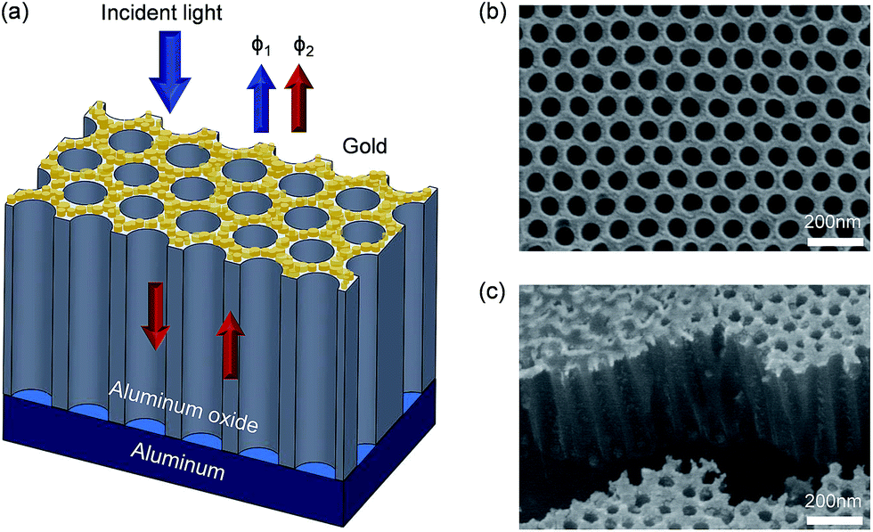 | ||
| Fig. 1 (a) Schematic illustration of the plasmonic AAO nanotemplate. The AAO template is grown on the aluminum substrate and the gold is sputtered on the AAO template. The thickness of the AAO template can be tuned by anodization time. The arrows show the incident and reflected light paths through the structure. (b) The scanning electron microscopy (SEM) image for the top of the AAO nanostructure shows a well-ordered hexagonal array with an average pore size of 70 nm and an average lattice between the pores of 100 nm. The gold layer of ∼10 nm was sputtered on the surface of the AAO template. The sputtered gold forms a nanosurface with small empty holes and a rough surface. (c) The side view SEM image of the AAO nanostructure shows that most of the gold is deposited on the surface of the AAO template and few gold particles are attached on the side walls. | ||
While the Fabry–Perot cavity mode is determined by the thickness of the AAO template, the strength of the coupling with the metal nanosurfaces depends on whether the metal nanosurfaces are located at the node or at the anti-node of the Fabry–Perot mode.40 In a typical Fabry–Perot cavity, their field localization is very poor so that the support of SPR is limited. However, our porous Fabry–Perot cavity structure increases the interaction length between the cavity and the infiltrated analyte, and the phase shifts ϕ1 and ϕ2 can be greatly affected by the SPR of the top metal nanosurfaces. In a thicker AAO structure, the phase accumulation is more important to keep several round trips of the light inside the microcavity.
Scanning electron microscopy (SEM) images show that the AAO template has a well-ordered hexagonal array with an average pore size of 70 nm and an average lattice between the pores of 100 nm, as shown in Fig. 1(b). The sputtered gold forms a rough surface on the surface of the AAO with an average thickness of 10 nm. The side view SEM image shows that most of the gold is deposited on the surface of the AAO template (Fig. 1(c)).
Using a commercial finite-difference time-domain (FDTD) package (Lumerical Solutions Inc.), we simulate reflectance spectra to find the resonant mode of the hybrid plasmonic AAO structure with respect to the cavity length. First, we assume that the pores in AAO are empty without the analyte. We also assume the sputtered gold nanosurfaces to be a uniformly deposited gold layer with a 10 nm thickness. Fig. 2(a) shows the normalized reflectance as a function of wavelength and of the AAO thickness. The reflectance spectrum modulations due to the Fabry–Perot modes can be clearly observed as a linear color region in the color contour map as functions of the AAO thickness and the wavelength. For a fixed AAO thickness, the reflectance spectrum shows modulated Fabry–Perot resonance conditions with increasing wavelength. Likewise, the modulation depth increases with the increased AAO thickness. At 638 nm, shown as a horizontal while dotted line, a sharp reflectance valley is observed. The reflectance valley corresponds to a destructive interference of the Fabry–Perot mode due to the gold nanosurface’s plasmon resonance.
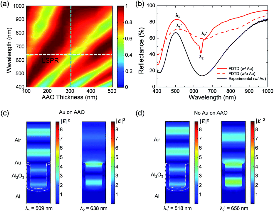 | ||
| Fig. 2 (a) Simulated normalized reflectance is shown as a color contour as a function of the thickness of the AAO template and the illumination wavelength for the cavity-coupled plasmonic structure described in Fig. 1. (b) Simulated (red) reflectance spectra by the finite-difference time-domain method and measured (black) spectrum are drawn with (solid) and without (dashed) the gold layer. The AAO template thickness is 300 nm. The sputtered gold layer on the AAO template enhances the modulation depth of the Fabry–Perot mode. Simulated electric field intensity distributions are shown with the gold layer (c) for the peak (λ1 = 509 nm) and the valley (λ2 = 638 nm), and without the gold layer (d) for the peak (λʹ1 = 518 nm) and the valley (λʹ2 = 656 nm), respectively. The plasmonic absorption is shown in (c) at the wavelength of the valley of the reflectance spectrum (λ2) near the gold layer. | ||
In order to find the effect of the sputtered gold nanosurfaces on the Fabry–Perot mode, we simulate reflectance spectra of 300 nm thick AAO microcavities for the cases with and without gold layers, as shown in Fig. 2(b). The red solid line and dotted line denote the simulated reflectance spectra of AAO with and without a thin gold layer, respectively. Without gold nanosurfaces, the Fabry–Perot mode of the pristine AAO template does not show any sharp modulation depth. The resultant FOM derived from the reflection peak (or valley) without gold nanosurfaces is low. On the other hand, the simulation shows a sharp negative peak near the valley at 638 nm due to the surface plasmon resonance (SPR) of gold. In addition, the reduced reflection at the valley further enhances the FOM.
Refractometric index sensing by hybrid plasmon-coupled AAO templates
We measured the reflection spectrum to find out the sharp negative peak at 638 nm. Unfortunately, this negative peak could not be experimentally observed, as seen from the black solid line in Fig. 2(b). According to our speculation, the negative peak is smeared out due to the imperfect hexagonal AAO lattice structure and non-uniform layer thickness. Without the sharp negative peak, though, the reduced reflection valley near 630 nm by gold sputtering leads to an enhanced FOM of the peak at 509 nm. We also note that the reflectance at 509 nm increases 10% for the AAO with gold nanosurfaces. The increased modulation depth of the Fabry–Perot mode is better for refractive index sensing.Mode profiles at the reflectance peaks and valleys are shown in Fig. 2(c) and (d) for the AAO with the gold layer (c) for the peak (λ1 = 509 nm) and valley (λ2 = 638 nm), and without the gold layer (d) for the peak (λʹ1 = 518 nm) and valley (λʹ2 = 656 nm), respectively. Regardless of the gold nanosurfaces, a standing wave pattern can be observed both inside and outside the AAO microcavity. Mode profiles at λ1 and λʹ1 show constructive interference allowing for large reflection from the AAO microcavity. Whereas the mode profiles at λ2 and λʹ2 show destructive interference and a highly confined mode within the AAO microcavity. Even though the field difference outside the cavity at λ1 and λʹ1 is not significant (10% change in Fig. 2(b)), the field difference outside the cavity at λ2 and λʹ2 is very large. Therefore, the reflectance spectrum modulation depth for the case with the gold nanosurfaces is larger than that for the case without the gold nanosurfaces. The enhanced modulation depth in the reflectance spectrum leads to a higher FOM for analyte index sensing.
In order to enhance the reflectance spectrum modulation depth, we increase the AAO hybrid cavity thickness to 500 nm for the refractometric sensing scheme. Cargille refractive index fluids, which are stable and wettable to the AAO surface, are used as test analytes to control the refractive index values 1.35 and 1.7.20 As analytes with a higher refractive index infiltrate into the AAO template, the reflection spectrum moves to a longer wavelength, pushing up the resonance condition of the hybrid plasmonic AAO structure changes, as shown in Fig. 3. Within the detector range in the visible region, the peaks at the longest wavelength show a large shift after the analyte infiltration. As a result, the peak shift is linearly proportional to the refractive index of the analytes with a maximum sensitivity of ∼324 nm per RIU.
 | ||
| Fig. 3 Refractometric index sensing using the plasmonic AAO nanostructure. Measured reflectance spectra of the plasmonic AAO nanostructure by changing the surrounding medium with a different refractive index (n = 1–1.7) when the AAO template thickness is 500 nm. The peaks are shifted to a longer wavelength with a constant rate as the refractive index of the surrounding medium increases. With this thickness of 500 nm of the AAO template, a sensitivity of ∼324 nm per RIU is obtained. The color images of the AAO templates with analytes are shown on the right. | ||
Colorimetric index sensing by the hybrid plasmon-coupled AAO templates
With the AAO template with infiltrated analyte, we observed significant color changes, suggesting that our AAO template can be used as a colorimetric sensor. The color of the prepared AAO microcavity is affected by all the interference peaks. Since the color depends on the cavity structure and the material’s dielectric permittivity, a refractive index change can be perceptually recognized by color gamut analysis.46 The color can be changed with respect to the viewing angle as well as the analyte refractive index.In order to figure out the best thickness for the colorimetric sensor, eight AAO templates with thicknesses from 100 nm to 360 nm have been examined regarding four different analytes with refractive indices from n = 1.40 to n = 1.70, as shown in Fig. 4. The 100 nm thick AAO sensor shows little color change, whereas the AAO sensors with a thickness from 180 nm to 330 nm show large color changes with the infiltrated analyte targets.
 | ||
| Fig. 4 Optical images of the AAO templates as a function of the tested refractive index immersion liquids and thickness of the AAO template from 100 nm to 360 nm. All images are taken by a digital camera at a normal viewing angle under identical illumination conditions. The color change with a 100 nm thick AAO microcavity is not noticeable, whereas those with a 180–330 nm thickness show vivid color changes. | ||
Based on the optical images taken by a digital camera, we evaluate the colorimetric sensing performance of our hybrid AAO microcavity by mapping the image data to a CIELab 1931 chromaticity diagram, as shown in Fig. 5. One of the advantages of the CIELab color representation is device-independence so that comparison with other photographed images is possible.47 All the colors in the CIELab coordinates can be represented by tristimulus values:46 lightness L* and chromaticities a* and b*. The lightness L* component closely matches the human perception of lightness. A quantitative color difference between the two colors, denoted by ΔE, meaning the Euclidean distance between the two color points, is given by the following formula:
 | (1) |
 | ||
| Fig. 5 CIELab points of the plasmonic AAO sensor are shown as a function of the refractive indices of analytes and various AAO template thicknesses ranging from 100 nm to 360 nm. With an increasing refractive index of the analytes, the measured (L*, a*, b*) color points rotate clockwise. | ||
As the refractive indices of the test analytes increase, the calculated tristimulus values move clockwise, as shown in Fig. 5. Therefore, an appropriate sensing device should be chosen for a specific analyte’s refractive index. Table 1 shows the calculated Euclidean distances for the refractive index change of the analytes. Because the tristimulus values do not monotonically increase with the increasing refractive index of the analytes, the actual path in the CIELab space along the continuous index change is longer than the Euclidean distance between two points. Therefore, the calculated RIU/ΔE is interpreted as the lower limit of the colorimetric sensing performance of our AAO microcavity. The AAO microcavities with 180–330 nm thicknesses show values no larger than RIU/ΔE = 0.01. The best perceptual refractive index change is RIU/ΔE ∼ 0.006 when Δn = 0.1.
| AAO thickness | ΔE | RIU/ΔE | |||
|---|---|---|---|---|---|
| n = 1–1.4 | n = 1.4–1.5 | n = 1.5–1.6 | n = 1.6–1.7 | ||
| 100 nm | 8.77 | 5.10 | 8.83 | 5.74 | 0.011 |
| 140 nm | 25.20 | 6.78 | 5.39 | 5.10 | 0.015 |
| 180 nm | 10.77 | 12.25 | 7.55 | 7.81 | 0.008 |
| 220 nm | 42.06 | 13.00 | 5.92 | 4.90 | 0.008 |
| 250 nm | 24.92 | 10.00 | 15.62 | 11.22 | 0.006 |
| 280 nm | 49.68 | 8.94 | 8.25 | 6.16 | 0.008 |
| 330 nm | 31.59 | 14.04 | 11.70 | 10.25 | 0.007 |
| 360 nm | 20.49 | 10.63 | 8.60 | 6.56 | 0.009 |
Enhanced FOM with increasing AAO thickness
As long as a good Fabry–Perot mode is maintained, the thicker AAO microcavity provides a greater number of modal peaks. This in turn leads to narrower peaks or valleys with the increased modulation depth. Therefore, increasing the anodizing time may pave the way to increase such a modulation depth and the FOM. The FOM is defined by FOM = (dλ/dn)/Δλ or (dEp/dn)/ΔEp depending on the domain unit.39 Here, Δλ and ΔEp are the FWHMs of a peak in the reflectance spectrum with the units for wavelength in nm and photon energy in eV, respectively.One of the major issues of increasing the cavity length is that the intensity of the total reflected light in the AAO microcavity decreases due to the light absorption and inelastic light scattering inside the AAO pores. For this purpose, good reflectivity at the top and bottom of the AAO template is necessary. We kept increasing the AAO thickness up to 5 μm as long as the gold nanosurface is coated on the top surface. As a result, the total reflection from the AAO template generates sharper interference peaks, as shown in Fig. 6(a). Without sputtered gold nanosurfaces, we find that the modulation depth of the AAO microcavity becomes poor, as shown in Fig. 6(b). Therefore, the peak shifts are not clearly recognized after analyte infiltration due to the broad reflectance peaks. The sputtered gold nanosurface on top of the AAO microcavity plays an important role of increasing the reflections and keeping the phase shifts. In addition, a stable Fabry–Perot mode and the resultant large FOM is achieved even with the imperfections of the AAO microcavity.
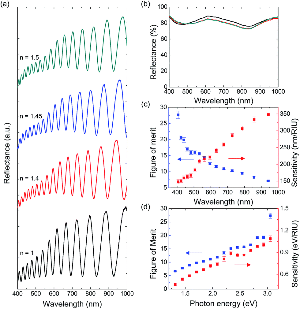 | ||
| Fig. 6 (a) Measured reflectance spectra of the plasmonic AAO nanostructure by changing the surrounding medium with a different refractive index (n = 1–1.5) when the AAO template thickness is 5 μm. (b) Reflectance spectra of the AAO structure without a gold layer. There are no changes as the refractive index of the surrounding medium increases. (c) Sensitivity and FOM of the plasmonic AAO nanostructure at the different peak center of AAO as a function of wavelength (nm). High sensitivities are obtained at longer wavelengths and high figures of merit are attained at shorter wavelengths. Although the sensitivity is getting lower as the peak wavelength decreases, the figure of merit increases due to the smaller FWHM. A maximum sensitivity of 348 nm per RIU is obtained. (d) Sensitivity and FOM of the same plasmonic AAO nanostructure as a function of photon energy (eV). They have the same trend in the energy domain. | ||
In order to compare the sensitivity and FOM in the same spectral domain, we plot the extracted sensitivities (red dots) and FOMs (blue dots) as a function of the wavelength and as a function of the photon energy, as shown in Fig. 6(c) and (d), respectively. In the wavelength domain, a sensitivity of up to 348 nm per RIU and a FOM of up to 27.7 can be obtained. One of the interesting features of the FOM in the wavelength domain is that the FOM behaves oppositely to the sensitivity, as shown in Fig. 6(c). This implies that the domain of the refractometric refractive index sensing should be more carefully chosen. In the energy domain as shown in Fig. 6(d), the sensitivities and FOMs follow the same trend. This means that the FOM gives better characteristics for refractive index sensing in the high energy region, i.e. in the short wavelength region. Even though the FOM serves as a kind of normalized unit-less sensitivity, only the FOM defined in the energy domain provides the same physical interpretation as the sensitivity.
Annealing effect of the hybrid plasmon-coupled AAO templates
We have attempted to enhance the color purity by annealing the gold nanosurface on the AAO template at 500 °C for 2 hours. The annealing leads to deformation of the sputtered gold nanosurface and to a color change due to the resultant phase change ϕ1 of the top interface, as shown in Fig. 7(a). SEM images taken before (b) and after (c) the annealing process show that the rough gold nanosurface transforms to nanoparticles. As the gold nanosurface transforms to nanoparticles, the plasmonic effect is enhanced while the gold-covered area is reduced. Consequently, the hybrid Fabry–Perot mode is changed. However, we find that the annealing does not produce a significant colorimetric performance enhancement. | ||
| Fig. 7 (a) Optical images of the AAO templates as a function of the thickness of AAO template from 100 nm to 360 nm before and after the annealing process. The annealing process was performed at 500 °C for 2 hours. All images were taken by a digital camera at a normal viewing angle under identical illumination conditions. Colors change for all thicknesses of AAO because the agglomerated gold particles developed by the annealing process enhance the localized surface plasmon resonance and reduce the Fabry–Perot interference. (b) SEM image of the plasmonic AAO nanostructure before the annealing process. (c) SEM image of the AAO nanostructure after the annealing process. Gold clusters agglomerate together to form nanoparticles with a diameter of 20–50 nm and smaller particles near the pores of the AAO template. | ||
Instead, we observe that annealing can enhance the refractometric sensing performance in a special condition. Fig. 8 shows the reflectance spectra change with an enhanced sensitivity for 280 nm thick AAO with the n = 1.4 analyte. The sensitivity from the shortest wavelength peak increases from 217 nm per RIU to 282 nm per RIU due to the annealing effect. However, AAO with other thicknesses ranging from 150 nm to 500 nm does not produce enhanced refractometric sensing performances. Further investigations are required for optimized annealing conditions for index sensing.
 | ||
| Fig. 8 Refractometric index sensing using the plasmonic AAO nanostructure of bare samples (solid lines) and annealed samples (dashed lines). Reflectance spectra of the plasmonic AAO nanostructure were measured in the air and in an infiltrating surrounding medium with a refractive index of 1.4 when the AAO template thickness is 280 nm. The peaks are shifted to a longer wavelength as the surrounding medium infiltrated and the annealed plasmonic AAO nanostructure shows more of a red-shift. The sensitivity from the shortest wavelength peak increases from 217 nm per RIU to 282 nm per RIU due to the annealing effect. | ||
Conclusions
In summary, we have introduced a facile approach to achieve a highly sensitive refractive index sensor using AAO nanostructures, which combines the advantages of Fabry–Perot microcavities with local surface plasmonic resonance induced by gold nanosurfaces. The reflectance spectrum under ambient illumination is linearly shifted due to the refractive index change of the infiltrated analyte with respect to the air. The gold nanosurfaces play significant roles to form hybrid resonances arising from the constructive and destructive interference. A high sensitivity and FOM were attained with a 5 μm AAO template for refractometric sensing. The FOMs of the spectra were examined to extract the most sensitive peak shift from the reflectance data: a sensitivity of 1.14 eV per RIU, and a FOM of 27.7 at an optical wavelength of around 406 nm. We observed that the sensitivity and FOM behave proportionally in the photon energy domain, but inversely in the wavelength domain with respect to the peak of the reflectance spectrum. The obtained highest sensitivity reaches 348 nm per RIU in the wavelength domain. Clear color changes by refractive index variation were achieved with an AAO template thickness of under 500 nm for the colorimetric sensing scheme. With the advantage of the proposed large-scale feature with a sensitive color change by simple infiltration of the analyte, we examined visually recognizable sensing characteristics by analysing CIELab mapping of the images taken by a conventional camera. Small refractive index changes down to ∼0.006 RIU can be obtained with respect to perceptual color change recognition over a whole visible range.Our sensor provides not only a refractometric sensing scheme with high sensitivity, but also a quite decent colorimetric sensing performance by the naked eye or cheap cameras for quick preliminary inspections. It is also possible to use it as a biosensor if receptors are pre-prepared either on top of or inside the AAO template for a selectivity function. The reflective phase shift of the Fabry–Perot mode can be changed by binding with analyte biomolecules. Since the mode change is proportional to the filling of the analyte inside the AAO pores, a liquid-type analyte seems unavoidable. If biomolecules in the air can be sufficiently condensed and the resultant index of the gas is changed, gaseous analytes might be applicable. Our approach is a promising candidate for low-cost and highly sensitive detection of multiple analytes in a simple and rapid format, and would have applications in other chemical systems, sensing for the food industry, and in IoT devices.
Acknowledgements
This research was supported by the Basic Science Research Program and the Pioneer Research Center Program through the National Research Foundation of Korea (NRF) funded by the Ministry of Science, ICT and Future Planning (NRF-2015R1A2A2A11001112, NRF-2013M3C1A3065045), the Low Observable Technology Research Center program of the Defense Acquisition Program Administration and Agency for Defense Development and an Asian Office of Aerospace R&D grant, FA2386-15-1-4024 (15IOA024). The authors gratefully thank to Yeon Hong Kim for careful feedback and discussions.References
- J. Homola, S. S. Yee and G. Gauglitz, Sens. Actuators, B, 1999, 54, 3–15 CrossRef CAS.
- A. J. Haes and R. P. van Duyne, J. Am. Chem. Soc., 2002, 124, 10596–10604 CrossRef CAS PubMed.
- J. Homola, Anal. Bioanal. Chem., 2003, 377, 528–539 CrossRef CAS PubMed.
- S. M. Borisov and O. S. Wolfbeis, Chem. Rev., 2008, 108, 423–461 CrossRef CAS PubMed.
- S. Zeng, K.-T. Yong, I. Roy, X.-Q. Dinh, X. Yu and F. Luan, Plasmonics, 2011, 6, 491–506 CrossRef CAS.
- X. Guo, J. Biophotonics, 2012, 5, 483–501 CrossRef CAS PubMed.
- I. Singh, International Journals of Nanosensors, 2015, 1, 1–7 Search PubMed.
- C. L. Baird and D. G. Myszka, J. Mol. Recognit., 2001, 14, 261–268 CrossRef CAS PubMed.
- W.-P. Chen, F.-H. Shih, P.-J. Tseng, C.-H. Shao and C.-C. Chiang, IEEE Sens. J., 2015, 15, 734–741 CrossRef.
- J. Lee, K. Bae, G. Kang, M. Choi, S. Baek, D. Yoo, C.-W. Lee and K. Kim, RSC Adv., 2015, 5, 71770–71777 RSC.
- M. Bahramipanah, M. S. Abrishamian, S. A. Mirtaheri and J.-M. Liu, Sens. Actuators, B, 2014, 194, 311–318 CrossRef CAS.
- J. Álvarez, C. Serrano, D. Hill and J. Martínez-Pastor, Opt. Lett., 2013, 38, 1058–1060 CrossRef PubMed.
- S.-H. Yeom, M.-E. Han, B.-H. Kang, K.-J. Kim, H. Yuan, N.-S. Eum and S.-W. Kang, Sens. Actuators, B, 2013, 177, 376–383 CrossRef CAS.
- H. M. Hiep, H. Yoshikawa and E. Tamiya, Anal. Chem., 2010, 82, 1221–1227 CrossRef CAS PubMed.
- A. Yamaguchi, K. Hotta and N. Teramae, Anal. Chem., 2009, 81, 105–111 CrossRef CAS PubMed.
- K. Hotta, A. Yamaguchi and N. Teramae, Anal. Chem., 2010, 82, 6066–6073 CrossRef CAS PubMed.
- K. Hotta, A. Yamaguchi and N. Teramae, ACS Nano, 2012, 6, 1541–1547 CrossRef CAS PubMed.
- B. Ai, Y. Yu, H. Möhwald and G. Zhang, Adv. Opt. Mater., 2013, 1, 724–731 CrossRef.
- Y. Dou, J. Han, T. Wang, M. Wei, D. G. Evans and X. Duan, J. Mater. Chem., 2012, 22, 14001–14007 RSC.
- M. Khorasaninejad, N. Abedzadeh, J. Walia, S. Patchett and S. S. Saini, Nano Lett., 2012, 12, 4228–4234 CrossRef CAS PubMed.
- M. Khorasaninejad, S. M. Raeis-Zadeh, H. Amarloo, N. Abedzadeh, S. Safavi-Naeini and S. S. Saini, Nanotechnology, 2013, 24, 355501 CrossRef PubMed.
- J. Homola, Chem. Rev., 2008, 108, 462–493 CrossRef CAS PubMed.
- M.-C. Estevez, M. A. Otte, B. Sepulveda and L. M. Lechuga, Anal. Chim. Acta, 2014, 806, 55–73 CrossRef CAS PubMed.
- R. Ameling, L. Langguth, M. Hentschel, M. Mesch, P. V. Braun and H. Giessen, Appl. Phys. Lett., 2010, 97, 253116 CrossRef.
- Y. Shen, J. Zhou, T. Liu, Y. Tao, R. Jiang, M. Liu, G. Xiao, J. Zhu, Z.-K. Zhou, X. Wang, C. Jin and J. Wang, Nat. Commun., 2013, 4, 2381 Search PubMed.
- J. N. Anker, W. P. Hall, O. Lyandres, N. C. Shah, J. Zhao and R. P. van Duyne, Nat. Mater., 2008, 7, 442–453 CrossRef CAS PubMed.
- L. Tong, H. Wei, S. Zhang and H. Xu, Sensors, 2014, 14, 7959–7973 CrossRef CAS PubMed.
- K. M. Mayer and J. H. Hafner, Chem. Rev., 2011, 111, 3828–3857 CrossRef CAS PubMed.
- A. G. Brolo, Nat. Photonics, 2012, 6, 709–713 CrossRef CAS.
- J. B. Lassiter, H. Sobhani, J. A. Fan, J. Kundu, F. Capasso, P. Nordlander and N. J. Halas, Nano Lett., 2010, 10, 3184–3189 CrossRef CAS PubMed.
- A. Christ, Y. Ekinci, H. H. Solak, N. a. Gippius, S. G. Tikhodeev and O. J. F. Martin, Phys. Rev. B: Condens. Matter Mater. Phys., 2007, 76, 201405 CrossRef.
- B. Gallinet and O. J. F. Martin, ACS Nano, 2011, 5, 8999–9008 CrossRef CAS PubMed.
- N. Liu, L. Langguth, T. Weiss, J. Kastel, M. Fleischhauer, T. Pfau and H. Giessen, Nat. Mater., 2009, 8, 758–762 CrossRef CAS PubMed.
- S. Zhang, D. Genov, Y. Wang, M. Liu and X. Zhang, Phys. Rev. Lett., 2008, 101, 047401 CrossRef PubMed.
- A. Farhang, T. Siegfried, Y. Ekinci, H. Sigg and O. J. F. Martin, J. Nanophotonics, 2014, 8, 83897 CrossRef.
- Z.-D. Zhang, H.-Y. Wang and Z.-Y. Zhang, Plasmonics, 2012, 8, 797–801 CrossRef.
- X.-P. Jin, X.-G. Huang, J. Tao, X.-S. Lin and Q. Zhang, IEEE Trans. Nanotechnol., 2010, 9, 134–137 CrossRef.
- D. Chanda, K. Shigeta, T. Truong, E. Lui, A. Mihi, M. Schulmerich, P. V. Braun, R. Bhargava and J. A. Rogers, Nat. Commun., 2011, 2, 479 CrossRef PubMed.
- M. A. Schmidt, D. Y. Lei, L. Wondraczek, V. Nazabal and S. A. Maier, Nat. Commun., 2012, 3, 1108 CrossRef PubMed.
- D. Choi, C. K. Shin, D. Yoon, D. S. Chung, Y. W. Jin and L. P. Lee, Nano Lett., 2014, 14, 3374–3381 CrossRef CAS PubMed.
- M. Bahramipanah, S. Dutta-Gupta, B. Abasahl and O. J. F. Martin, ACS Nano, 2015, 9, 7621–7633 CrossRef CAS PubMed.
- G. Kang, J. Yoo, J. Ahn and K. Kim, Nano Today, 2015, 10, 22–47 CrossRef CAS.
- H. Masuda and M. Satoh, Jpn. J. Appl. Phys., 1996, 35, L126 CAS.
- G. Kang, K. Bae, M. Nam, D.-H. Ko, K. Kim and W. J. Padilla, Energy Environ. Sci., 2015, 8, 2650–2656 CAS.
- H. Masuda and K. Fukuda, Science, 1995, 268, 1466–1468 CAS.
- J. Schanda, Colorimetery: Understanding the CIE System, John Wiley & Sons, 2007 Search PubMed.
- M. M. Hawkeye and M. J. Brett, Adv. Funct. Mater., 2011, 21, 3652–3658 CrossRef CAS.
Footnote |
| † Electronic supplementary information (ESI) available. See DOI: 10.1039/c5ra17637a |
| This journal is © The Royal Society of Chemistry 2015 |