Stabilization of Si microwire arrays for solar-driven H2O oxidation to O2(g) in 1.0 M KOH(aq) using conformal coatings of amorphous TiO2†
Matthew R.
Shaner
ab,
Shu
Hu
ab,
Ke
Sun
ab and
Nathan S.
Lewis
*abcd
aDivision of Chemistry and Chemical Engineering, California Institute of Technology, Pasadena, CA 91125, USA. E-mail: nslewis@caltech.edu
bJoint Center for Artificial Photosynthesis, California Institute of Technology, Pasadena, CA 91125, USA
cBeckman Institute Molecular Materials Research Center, California Institute of Technology, Pasadena, CA 91125, USA
dKavli Nanoscience Institute, California Institute of Technology, Pasadena, CA 91125, USA
First published on 5th November 2014
Abstract
Conductive, amorphous TiO2 coatings deposited by atomic-layer deposition, in combination with a sputter deposited NiCrOx oxygen-evolution catalyst, have been used to protect Si microwire arrays from passivation or corrosion in contact with aqueous electrolytes. Coated np+-Si/TiO2/NiCrOx as well as heterojunction n-Si/TiO2/NiCrOx Si microwire-array photoanodes exhibited stable photoelectrochemical operation in aqueous ferri-/ferro-cyanide solutions. The coatings also allowed for photoanodic water oxidation in 1.0 M KOH(aq) solutions for >2200 h of continuous operation under simulated 1 Sun conditions with ∼100% Faradaic efficiency for the evolution of O2(g).
Broader contextPhotoelectrochemical conversion of sunlight into hydrogen has the ability to provide continuous, carbon-free energy, but in order to be an economically competitive energy source the system must be both efficient and stable for years of operation. This combination proves challenging as the most efficient semiconductors for solar-energy conversion are unstable after only seconds to minutes of operation, especially under oxidizing conditions. Accordingly, improving the stability while maintaining efficient operation is an important goal in furthering this technology and is the subject herein as demonstrated by a two-step approach. First, increasing the electrochemically active versus geometrical surface area with a periodically structured Si microwire array decreases the effective current density at the solid/solution interface and thus the rate of corrosion. Secondly, a conformal, transparent, electrically conductive protection layer serves as a corrosion-resistant barrier between the semiconductor and solution while maintaining efficient charge transfer to the reaction site. |
Technologically important, small band-gap semiconductors such as Si are highly attractive materials for use as photoanodes to oxidize water, but are unstable to corrosion and/or passivation under anodic conditions in aqueous electrolytes.1 Single crystalline n-Si, n-GaAs, n-GaP, n-CdTe, and n-BiVO4 photoanodes have all recently demonstrated enhanced stability (4–100+ hours) under continuous operation for water oxidation to O2(g) in aqueous alkaline electrolytes, with 100% Faradaic efficiency, by use of electrically conductive, optically transparent, 10–100 nm thick protective films of amorphous TiO2 deposited by atomic-layer deposition (ALD).2–4 Arrays of semiconductor microwires or nanowires provide an especially attractive system architecture for the direct production of fuels from sunlight, because such a structure provides a minimal path for ionic conduction, high optical absorption,5–9 a high surface-area support for electrocatalyst loading,10 and other distinctive, advantageous operational features.11 The application of conformal protective films to such highly anisotropic structures by use of sputtering or evaporation is expected to be difficult, whereas the self-limiting ALD surface condensation reaction technique is a conformal coating process. Accordingly, we describe herein the use of ALD-deposited amorphous TiO2 films to enable the continuous oxidation of water to O2(g) by Si microwire array photoanodes for >2200 h in 1.0 M KOH(aq) under simulated 1 Sun illumination conditions.
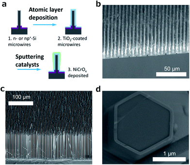
To fabricate the structures of interest, arrays of n-type and np+-radial junction Si microwires were coated with ALD-grown TiO2,4 followed by deposition of a nickel–chromium oxide oxygen-evolution catalyst using magnetron sputtering (see the ESI† for full Experimental details). Fig. 1a shows a schematic of the process, and Fig. 1b and c show scanning-electron micrographs (SEM) of the Si microwire arrays before and after deposition of the TiO2 protective coating (2000 ALD cycles, ∼94 nm) and the NiCrOx catalyst layer (20 min sputtering, ∼40 nm planar equivalent), respectively. Fig. 1d shows a cross-section near the base of a single fully processed (np+-Si/TiO2/NiCrOx) microwire within an array, demonstrating that the fabrication produced the desired structure as well as a conformal layer of TiO2 having a relatively uniform thickness along the height of the wire. A detailed inspection of an individual Si microwire indicated that the NiCrOx deposited at the top and base of each Si microwire, due to the relatively line-of-sight deposition profile of the magnetron sputtering process. Only the regions of the NiCrOx catalyst on the surfaces of the wires are expected to be electrocatalytically active, due to the electrically insulating SiO2 on the sample substrate.
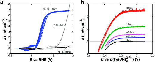
Fig. 2 shows the current density vs. potential (J–E) behavior of an np+-Si/TiO2/NiCrOx microwire-array photoelectrode in contact with (a) 1.0 M KOH(aq) (pH = 13.6) and (b) 0.50 M K2SO4–0.050 M K3Fe(CN)6–0.35 M K4Fe(CN)6(aq) in the presence and absence, respectively, of 100 mW cm−2 of simulated Air Mass (AM) 1.5G illumination. Fig. 2a also depicts the J–E behavior of a p+-Si/TiO2/NiCrOx microwire-array electrode in the absence of illumination, to allow for a comparison of the onset potentials for the oxygen-evolution reaction between the illuminated photoanode and a degenerately doped unilluminated p+-Si anode. The one-electron, outer-sphere, reversible Fe(CN)63−/4− redox couple was used to measure the intrinsic energy-conversion properties of the microwire-array photoanodes. Under 100 mW cm−2 of simulated Air Mass (AM) 1.5G illumination, the np+-Si/TiO2/NiCrOx microwire array produced an open-circuit potential (Eoc) of −0.62 V vs. the formal potential for water oxidation, E0′(O2/OH−), and a light-limited photocurrent density (Jph) of 7.1 mA cm−2 in 1.0 M KOH(aq), and produced Eoc = −0.44 V vs. the Nernstian potential of the solution (E(Fe(CN)63−/4−)) and Jph = 7.3 mA cm−2 in contact with Fe(CN)3−/4−(aq). A diode quality factor of 1.9–2.2 was measured in contact with Fe(CN)3−/4−(aq) from the J–E data obtained as a function of illumination intensity.5,12 The intrinsic photoelectrode behavior observed for the np+-Si/TiO2/NiCrOx photoanode in contact with the one-electron, reversible, Fe(CN)63−/4− redox system (Fig. 2b) demonstrated an energy-conversion efficiency of 1.8% with a fill factor of 0.54.
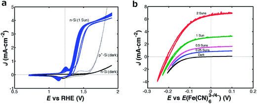
For comparison, Fig. 3 shows the J–E behavior in the presence and absence of illumination, respectively, of n-Si/TiO2/NiCrOx microwire-array photoelectrodes in (a) 1.0 M KOH and (b) an aqueous Fe(CN)63−/4− solution. In contact with 1.0 M KOH(aq), these samples exhibited Eoc = −0.49 V vs. E0′(O2/OH−) and Jph = 3.7 mA cm−2 (Fig. 3a), whereas in contact with Fe(CN)63−/4−(aq) the n-Si/TiO2/NiCrOx microwire arrays exhibited Eoc = −0.18 V vs. E(Fe(CN)63−/4−) and Jph = 3.1 mA cm−2. The intrinsic photoelectrode behavior observed for the n-Si/TiO2/NiCrOx photoanode in contact with the Fe(CN)63−/4− redox system (Fig. 2b) demonstrated an energy-conversion efficiency of 0.3% with a fill factor of 0.51. When measured under nominally identical conditions, all (6 electrodes) of the microwire-array photoelectrodes studied herein showed mutually similar photovoltages, but exhibited variable photocurrent densities with a spread of ∼5 mA cm−2, consistent with a variation in wire height at various locations on the wafer from which the electrodes were fabricated.13,14 The addition of scattering particles can significantly increase Jph by increasing the illumination path length through the photoactive Si microwire array.15
Fig. 4a shows the external quantum yield (Φext) for np+-Si/TiO2/NiCrOx and n-Si/TiO2/NiCrOx microwire-array photoelectrodes in contact with 1.0 M KOH(aq). The observed behavior was similar to that obtained previously for microwire-array photocathodes and photovoltaics illuminated at normal incidence.15 The Φext exhibited a similar dependence on wavelength for both the np+-Si and the n-Si microwire arrays, consistent with behavior dominated by absorption and charge-carrier collection in a microwire array. Integration of the wavelength-dependent spectral response data of protected np+-Si and n-Si microwire-arrays with respect to the AM 1.5G solar spectrum yielded calculated photocurrent densities of 7.9 mA cm−2 and 2.9 mA cm−2, respectively, in excellent agreement with the Jph values measured from the J–E behavior.
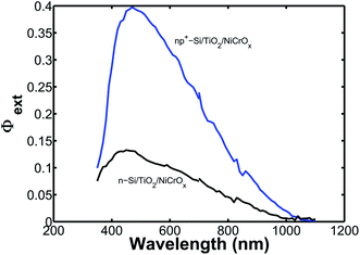 | ||
| Fig. 4 External quantum yield (Φext) versus wavelength plot of representative protected n-Si and np+-Si microwire-array photoelectrodes in contact with 1.0 M KOH(aq). | ||
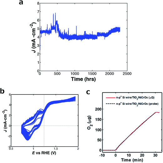
Fig. 5a shows the time dependence of the photocurrent density of an np+-Si microwire array under potentiostatic control at 0.36 V vs. E0′(O2/OH−) (0.70 V vs. a Hg/HgO reference electrode). Fig. 5b shows the J–E data at 10 h intervals throughout the stability test, showing no significant change in Jph, Eoc or fill factor during the stability evaluation. As shown in Fig. 5c, a comparison between the amount of O2(g) expected based on Coulomb's law and the amount of O2(g) detected using a calibrated fluorescent O2(g) probe indicated ∼100% Faradaic efficiency for oxygen evolution. Assuming four electrons per Si atom dissolved, the total number of coulombs of charged passed during the stability test, 6000 C, exceeded by a factor of 20 the 300 C of charge that would have been required to dissolve the entire Si microwire array. Furthermore, assuming that 10 nm of oxide formation would result in complete passivation of the electrode, the amount of charge passed establishes a lower limit of 9 × 10⁴ on the branching ratio for water oxidation to O2(g) relative to oxidation of the Si.
Accounting for the ∼20% capacity factor of sunlight, the 2200 h of continuous operation contained the same amount of charge as would be passed during >1 year of outdoor operation. Because lower current densities away from peak illumination times of day would likely increase the stability, this projected >1 year stability plausibly represents a lower limit on the actual stability of the NiOx-coated Si photoanodes under operational conditions. A detailed failure analysis study and validated accelerated testing protocols, additionally incorporating possible effects of temperature cycling and extended periods of no photocurrent current due to day/night cycling, would clearly be required to establish the ultimate limit on the stability of the photoanodes described herein. The high internal surface area of a highly anisotropic structure such as a microwire array produces a correspondingly low current density at the areas exposed to the electrolyte. This low current density is expected to beneficially reduce the rate of light-intensity-dependent photocorrosion or photopassivation processes, because the photon flux per projected geometric area provided by sunlight produces minority-carrier currents that are distributed over a large internal surface area of the solid/liquid contact in the internal volume of a microwire array. Consistently, the microwire arrays exhibited a greater degree of stability than crystalline Si electrodes protected by amorphous TiO2 films and operated at 30 mA cm−2, which exhibited a small but significant decay in photocurrent after 24 h of continuous operation in the same electrolyte.4 Incorporation of the np+-Si/TiO2/NiCrOx photoanode into a complete water-splitting device operating at 10% solar-to-hydrogen efficiency would require a photocathode capable of producing >10 mA cm−2 at 1.5 V and addition of scattering particles to increase the absorption and current density in the Si microwires.15 For efficient operation, such a photocathode, operating near its Shockley–Quiesser limit, would need to have a band gap of ∼2.0 eV with either a buried junction or proper band positioning relative to the hydrogen-evolution potential. The observations reported herein therefore illustrate an additional advantage of the amorphous TiO2-based protection strategy in that the deposition method, ALD, is especially well suited to be compatible with a wide range of high-efficiency materials while also being compatible with a broad range of morphologies associated with highly anisotropic structures of the light absorber.
Acknowledgements
The authors would like to acknowledge Dr Ragip Pala for assistance with the spectral response measurement system. This material is based upon work performed by the Joint Center for Artificial Photosynthesis, a DOE Energy Innovation Hub, supported through the Office of Science of the U.S. Department of Energy under Award Number DE-SC0004993. M. R. S. is supported by a graduate fellowship from the Resnick Institute for Sustainability. The authors also acknowledge support from the Gordon and Betty Moore Foundation.Notes and references
- J. R. McKone, N. S. Lewis and H. B. Gray, Chem. Mater., 2014, 26, 407–414 CrossRef CAS.
- M. F. Lichterman, A. I. Carim, M. T. McDowell, S. Hu, H. B. Gray, B. S. Brunschwig and N. S. Lewis, Energy Environ. Sci., 2014, 7, 3334–3337 CAS.
- M. T. McDowell, M. F. Lichterman, J. M. Spurgeon, S. Hu, I. D. Sharp, B. S. Brunschwig and N. S. Lewis, J. Phys. Chem. C, 2014, 118, 19618–19624 CAS.
- S. Hu, M. R. Shaner, J. A. Beardslee, M. Lichterman, B. S. Brunschwig and N. S. Lewis, Science, 2014, 344, 1005–1009 CrossRef CAS PubMed.
- S. Hu, C.-Y. Chi, K. T. Fountaine, M. Yao, H. A. Atwater, P. D. Dapkus, N. S. Lewis and C. Zhou, Energy Environ. Sci., 2013, 6, 1879 CAS.
- A. R. Madaria, M. Yao, C. Chi, N. Huang, C. Lin, R. Li, M. L. Povinelli, P. D. Dapkus and C. Zhou, Nano Lett., 2012, 12, 2839–2845 CrossRef CAS PubMed.
- J. Zhu, Z. Yu, G. F. Burkhard, C.-M. Hsu, S. T. Connor, Y. Xu, Q. Wang, M. McGehee, S. Fan and Y. Cui, Nano Lett., 2009, 9, 279–282 CrossRef CAS PubMed.
- A. Chutinan and S. John, Phys. Rev. A, 2008, 78, 023825 CrossRef.
- T. Tayagaki, Y. Hoshi, Y. Kishimoto and N. Usami, Opt. Express, 2014, 22, A225 CrossRef PubMed.
- E. L. Warren, J. R. McKone, H. A. Atwater, H. B. Gray and N. S. Lewis, Energy Environ. Sci., 2012, 5, 9653 CAS.
- S. Haussener, C. Xiang, J. M. Spurgeon, S. Ardo, N. S. Lewis and A. Z. Weber, Energy Environ. Sci., 2012, 5, 9922–9935 CAS.
- S. M. Sze and K. K. Ng, Physics of Semiconductor Devices, Wiley-Interscience, 3rd edn, 2006 Search PubMed.
- S. M. Eichfeld, H. Shen, C. M. Eichfeld, S. E. Mohney, E. C. Dickey and J. M. Redwing, J. Mater. Res., 2011, 26, 2207–2214 CrossRef CAS.
- E. L. Warren, H. A. Atwater and N. S. Lewis, J. Phys. Chem. C, 2014, 118, 747–759 CAS.
- M. D. Kelzenberg, S. W. Boettcher, J. A. Petykiewicz, D. B. Turner-Evans, M. C. Putnam, E. L. Warren, J. M. Spurgeon, R. M. Briggs, N. S. Lewis and H. A. Atwater, Nat. Mater., 2010, 9, 239–244 CrossRef CAS.
Footnote |
| † Electronic supplementary information (ESI) available: Experimental methods and supplementary data. See DOI: 10.1039/c4ee03012e |
| This journal is © The Royal Society of Chemistry 2015 |

