
Routes to tin chalcogenide materials as thin films or nanoparticles: a potentially important class of semiconductor for sustainable solar energy conversion
David J.
Lewis
*ab,
Punarja
Kevin
a,
Osman
Bakr
c,
Christopher A.
Muryn
a,
Mohammad Azad
Malik
a and
Paul
O'Brien
*ab
aSchool of Chemistry, The University of Manchester, Oxford Road, Manchester, M13 9PL, Northern Ireland, UK. E-mail: Paul.O'Brien@manchester.ac.uk; david.lewis-4@manchester.ac.uk; Tel: +44 (0)161 275 4653
bSchool of Materials, The University of Manchester, Oxford Road, Manchester, M13 9PL, Northern Ireland, UK
cKing Abdullah University of Science and Technology (KAUST), Thuwal, Saudi Arabia
First published on 5th August 2014
Abstract
Thin films of tin chalcogenides may find use in photovoltaic devices, and nanocrystals of such materials are attractive due to their tuneable band gaps and potential in photovoltaic, photonic and optoelectronic applications. Tin(II) sulfide (SnS) is of particular interest due to its band gap of 1.4 eV, which is similar to that of silicon (1.1 eV). This review seeks to provide an overview of the chemical routes currently known for the synthesis of tin chalcogenides as thin films or in nanocrystalline form, as well as exploring routes to copper zinc tin sulfide (CZTS) and mesoporous tin chalcogenides.
 David J. Lewis | David J. Lewis obtained his Ph.D. in 2006 from the University of Birmingham, U.K. This was followed by a short sojourn in industry as a process chemist (2006–2009). DJL returned to the University of Birmingham to work under Professor Zoe Pikramenou, developing luminescent nanoparticles for flow velocimetry measurements in collaboration with Professor Panagiota Angeli, University College London. In 2013, DJL took up his current position as a research associate under Professor Paul O'Brien FRS at The University of Manchester, U.K., as part of the newly established BP International Centre for Advanced Materials (BP-ICAM), working towards the understanding and development of inorganic lubricant additives for automotive engines. In league with Professor O'Brien, DJL has also recently developed a novel ambient-pressure route toward the deposition of inorganic–organic perovskites, potentially important for next-generation photovoltaic device manufacture. DJL is a Member of the Royal Society of Chemistry. |
 Punarja Kevin | Punarja Kevin is a final year PhD student in the School of Chemistry at the University of Manchester. She holds a Graduate Diploma in IT (1998) from ER&DCI, India, a B.Sc. in Chemistry, Physics and Mathematics (1999) from the University of Kerala, India, MSC chemistry (2001) from Govt. Of Kerala, India, Bachelors in Education (2002) MG Uty, India, SET (2002) and PG in Business Management (2011) from London School of Business Management, U.K. She was appointed as a junior lecturer in Chemistry by the Government of Kerala in July 2002. From 2009 she took on an additional role as a state resource group member in chemistry under the Directorate of Higher Education, Government of Kerala, India. Since 2012 she has been studying for a Ph.D. under the supervision of Professor Paul O'Brien FRS, in the development of precursors for the preparation of semiconductor nanoparticles and thin films for photovoltaic and optoelectronic applications. |
 Osman Bakr | Osman M. Bakr is an Assistant Professor of Materials Science and Engineering, SABIC Presidential Career Development Chair, at King Abdullah University of Science and Technology (KAUST), Saudi Arabia. He holds a B.Sc. in Materials Science and Engineering from MIT (2003) as well as a M.S. and Ph.D. in Applied Physics from Harvard University (2009). He was a postdoctoral fellow in the Laboratory for Nanoscale Optics at Harvard University. In 2010 he moved to KAUST and founded the Functional Nanomaterials Lab, a research group dedicated towards the study of nanoparticles and quantum dots; particularly advancing their synthesis and self-assembly for applications in photovoltaics, optoelectronics, and photocatalysis. |
 Christopher A. Muryn | Christopher A. Muryn is Head of Research and Analytical Services in the School of Chemistry, The University of Manchester. He holds a B.Sc. in Chemical Physics (1986) as well as a M.Sc. in Instrumentation and Analytical Science (1987) from UMIST. He obtained a PhD in Surface Science from Manchester University (1991). He was then a post-doctoral research associate in the Interdisciplinary Research Centre for Surface Science, University of Liverpool followed by Senior Experimental Officer (1991–1997). Then an SEO at Manchester University until 2010 where initially he continued his involvement in surface science until 2003, when he moved into X-ray crystallography. He became Head of Research and Analytical services in 2009 and has continued his research interests in surface science through synchrotron studies of rutile TiO2 primarily concerned with fundamental catalytic investigations. Whilst also supporting numerous research projects within the University, with X-ray diffraction and surface imaging techniques employing atomic force microscopy and scanning tunneling microscopy. |
 Mohammad Azad Malik | Mohammad Azad Malik completed his Ph.D. degree at the University of London in 1990 and then worked with Professor Paul O'Brien FRS initially at Queen Mary, University of London (1990–1995), then Imperial College (1995–2000), and currently The University of Manchester (2000 to 2014). He has been involved in various fields of research and has over 100 peer-reviewed articles on topics including single-source molecular precursors for II/VI, III/V, III/VI, and IV/VI semiconductors, MOCVD, AACVD, CBD, and the colloidal synthesis of nanoparticles. He was recently appointed as an independent research fellow at the University of Manchester (2014-present). |
 Paul O'Brien | Paul O'Brien FRS is Chair of Inorganic Materials Chemistry in the Schools of Chemistry and of Materials at the University of Manchester; he was Research Dean (2000–2003), Head of the School of Chemistry (2002–2009) and is now Head of the School of Materials. He held academic positions at Chelsea, Queen Mary and Imperial Colleges in the University of London. External appointments have included: Vice-President of the RSC (2009–2011), visiting Professor at Georgia Tech (1996–1999), visiting Fellow Magdalen College, University of Oxford (2009) and Distinguished Fellow at the Institute for Advanced Studies, Durham (2011). He has received distinguished alumni awards: the Potts Medal (Liverpool) and the A. G. Evans Memorial Medal Lecture (Cardiff). He was also awarded the Kroll, Sir Colin Humphreys and the Platinum medals of the IOMMM and the first Peter Day Award from the RSC. His research centres on developing new chemical processes for semiconducting thin films and nanoparticles, especially those comprised of metal chalcogenides. He has authored ca. 600 peer-reviewed publications (h > 55) as well as being the editor of a number of books and specialist periodical reports. He holds honorary D.Sc. degrees from both the Universities of Zululand and Liverpool. In 2002 he founded Nanoco, now listed on AIM/LSE. In 2013 he was elected a Fellow of the Royal Society, London. |
1. Introduction
Tin is a group IV element typically classified as a hard acid in Pearson's hard-soft acid–base (HSAB) paradigm. There is interesting redox chemistry and both tin(II) and tin(IV) species, and its organometallic and metal–organic complexes are stable, it also has a wide-range of alloy compositions with various properties. Tin chalcogenides of the type SnE where E = S, Se or Te have recently attracted considerable interest due to their semiconducting properties. Typically, these materials are observed to have intense absorption across the electromagnetic (EM) spectrum, and narrow band gaps and they therefore have potential as materials for optoelectronic and photovoltaic applications. A summary of band gaps in relation to the atmospheric solar spectrum is presented in Scheme 1. Tin is a far less toxic and, indeed, a relatively earth-abundant metal compared with many of other elements used in semiconductor materials. There has been great interest in the controlled deposition of thin films of tin chalcogenides and the synthesis of tin chalcogenide nanocrystals of controlled size and shape with tuneable band gaps. | ||
| Scheme 1 The optical band gaps of selected semiconductors with respect to the atmospheric solar emission spectrum. | ||
Photovoltaic cells are devices that convert photons into direct-current electricity by the photovoltaic effect. Solar cells rely on an absorber layer that can absorb photons and produce an exciton (electron–hole pair) that can be separated in space to produce an electrical current in a circuit. In this sense, photovoltaic cells act as diodes in parallel with a current source.1 Measurement of the current vs. voltage behaviour under illumination allows the characteristics of the photovoltaic cell to be determined. The maximum current possible is known as the short circuit current (ISC) whilst the maximum voltage occurs at open circuit (VOC). The overall power conversion efficiency (PCE, η) is defined as the ratio of the optical power in and the electrical power out:

The so-called fill factor (FF) of a photovoltaic cell is defined as the ratio of the maximum electrical power to the product of the short circuit current and open circuit voltage so that:

And thus the PCE of a photovoltaic cell can be defined as:

Tin sulfide is a promising material for the absorber layer in solar cells, primarily due to the earth-abundant elements comprising the material but secondly it has an optical band gap commensurate with that of silicon (1.1 eV). It absorbs light across the visible spectrum, typically with absorption coefficients of the order of 104–105 (Fig. 1). The highest efficiency for a solar cell using SnS as an absorber layer was recently reported by Gordon and co-workers to be 4.4% under standard test conditions,2 though this PCE is far from optimal; theoretical PCEs for SnS are ca. 24%.3
 | ||
| Fig. 1 Local Sn environments in (a) SnS, (b) SnS2 and (c) Sn2S3; and Sn⋯S connectivity in (d) SnS, (e) SnS2 and (f) Sn2S3. (Sn(II)-grey, Sn(IV)-violet, S-yellow). Reprinted with permission from Ramasamy et al., Chem. Mater., 2013, 25, 266–276. Published 2013 American Chemical Society. | ||
This review outlines methods for the deposition of thin films of binary tin chalcogenides, specifically the sulfides (SnS), selenides (SnSe) and tellurides (SnTe), as well as covering methods to make their nanocrystalline analogues. We outline some of the latest research into the quaternary tin chalcogenide material copper zinc tin sulfide, Cu2ZnSnS4 (CZTS), which is a potentially low-cost and sustainable material for solar energy conversion. We also detail research into mesostructured tin chalcogenide materials. The applications for these materials are discussed on a case-by-case basis. The reader should gain a sense of the avant garde as well as new and future directions in this field.
2. Tin sulfides
Tin sulfides are a class of IV–VI semiconductors which exists in three main forms: SnS, SnS2 and Sn2S3. Tin can take co-ordination numbers from 2 to 9 and often displays varying bonding preferences, commonly tetrahedral, trigonal bipyramidal and octahedral for tetravalent tin.The structures of orthorhombic SnS, SnS2 and Sn2S3 give unambiguous information regarding the arrangement of atoms around the Sn2+ and Sn4+ ions in the different types of tin sulfide (Fig. 1). SnS crystallizes in a deformed NaCl structure (herzenbergite) containing double layers of Sn and S atoms which are tightly bonded. The layers are weakly held together by van der Waals forces. Each Sn2+ ion is bonded to six sulfur atoms in a distorted octahedral geometry, with three short (ca. 2.7 Å) and three long (ca. 3.4 Å) bonds in an octahedral configuration. Interestingly, SnS is known to undergo a transformation from a GeS to a TlI-type structure above 605 °C with movement of Sn and S along the [100] direction, caused apparently by thermal expansion.
Tin disulfide (SnS2) most often exists in the PbI2 layered structure in which the Sn4+ centres are coordinated to six sulfur atoms at ca 2.6 Å. The layers are comprised of edge-sharing octahedral SnS6 units, which stack along the crystallographic c-axis with weak van der Waals interactions. A rich coordination chemistry of tin sulfides has been developed and has been discussed by Ozin et al.4 The polytypism observed in SnS2 leads to over seventy different forms with hcp layers, but with varying c parameters in the unit cell.4 Sn2S3 is a mixed valence compound with ribbon like structure. The Sn2+ ion is coordinated with sulfur in a trigonal bipyramidal geometry through two Sn–S distances of ca. 2.6 Å and ca. 2.7 Å. The Sn4+ sites in the ribbon are octahedrally coordinated with Sn–S distances of ca. 2.5–2.6 Å.
Tin sulfides have attracted attention as sustainable low-cost materials for photovoltaic solar energy absorbers. The bulk band gaps of the tin sulfides SnS, SnS2 and Sn2S3 are 1.4 eV, 2.3 eV and 1.1 eV respectively.5 All the forms of tin sulfides exhibit semiconducting properties, though as alluded to above SnS has attracted most attention due to its direct electronic band gap of 1.4 eV which is commensurate with the current industry-standard semiconductors silicon and gallium arsenide (Scheme 1).
2.1. Synthetic routes to tin sulfide thin films
A myriad of methods have been reported for the controlled deposition of tin sulfide thin films. Ray et al. reported the synthesis of tin(II) and tin(IV) sulfide thin films by dip deposition.6 Glass substrates were immersed in an methanolic solution of tin(II) chloride and thiourea followed by annealing at either 300 °C or 360 °C to produce the films. Optical measurements of the films established band gaps of 1.4 eV and 2.4 eV for SnS and SnS2 films respectively by photoconductivity measurements. Transmission spectra of SnS films demonstrated their absorbance over the majority of the visible spectrum (Fig. 2). | ||
| Fig. 2 Visible transmission spectrum of SnS films produced by Ray et al. using dip deposition.6 Reprinted from Ray et al., Thin Solid Films, 1999, 350, 72–78. Copyright 1999 with permission from Elsevier. | ||
The films were observed to be granular in appearance by SEM. Abou Shama et al. used thermal evaporation to deposit thin films of SnS on glass substrates at two temperatures.7 In this technique, a beam of electrons is targeted at the precursor materials immobilised on a substrate. The kinetic energy of the electrons is partially converted to thermal energy on impact, and the precursor components mutually decompose to the product. Analysis of films by powder XRD showed that films deposited at 27 °C were amorphous whilst those deposited at 145 °C were crystalline. Band gaps of 1.4 eV (indirect) and 2.2 eV (direct) for the amorphous films and 1.4 eV (indirect) and 2.3 eV (direct) for annealed crystalline films were determined.
Chemical bath deposition (CBD) is a cheap and versatile method for the large-area deposition of thin films relying on the spontaneous decomposition of precursors in solution to coat an immersed substrate. Variables such as bath temperature and solution pH can be adjusted to tune deposition. Ultrasonication can also be used to modulate the process. Ristov et al. used CBD to deposit SnS thin films onto glass substrates using a two-bath process with separate aqueous solutions of tin(II) chloride and either Na2S or (NH4)2S. The substrate was first immersed at room temperature in a solution of the sulfur source, followed by immersion in a bath of the metal salt at 80–90 °C.8 Nair et al. deposited SnS thin films at 60 °C from a 5% acetone solution in water containing tin(II) chloride and thioacetamide as the precursors with a mixture of amines.9 Engelken et al. used elemental sulfur and tin(II) chloride to deposit SnS thin films at 90 °C from propionic acid solution.10 Tanusevski prepared SnS thin films from tin(II) chloride and sodium thiosulfate in water at pH 7 with a post-deposition annealing at 250–300 °C.11 Gao and co-workers used CBD and the same tin and sulfur sources to investigate the influence of deposition temperature in the range 60–80 °C and precursor concentration ratios on the morphologies, compositions and optoelectronic properties of the deposited SnS thin films.12 It was found that high temperatures were detrimental to film compactness, whereas increasing the S to Sn ratio in the precursor mixture increased the compactness. The dark conductivities and photoconductivities of the films were found to increase with deposition temperature and S to Sn ratio. Band gaps in the range 1.0–1.3 eV were measured, with optical absorption edges located in the range 950–1200 nm with intense absorbance across the visible and near-infrared regions of the electromagnetic spectrum (Fig. 3), of importance for photovoltaic applications.
 | ||
| Fig. 3 Combined transmittance-reflectance curves for SnS films produced by Gao and co-workers by chemical bath deposition with band gaps in the range 1.0–1.3 eV.12 Reprinted from Gao et al., Thin Solid Films, 2012, 520, 3523–3527. Copyright 2012 with permission from Elsevier. | ||
Direct chemical vapour transport (CVT) was used by Arora et al. to grow crystalline thin films of SnS2 using stoichiometric amounts of elemental tin and sulfur as the precursors and traces of iodine to assist transport.13 The elements were heated to over 600 °C in a sealed vessel which was cooled extremely slowly to deposit the crystals. Crystal growth was found to be greatly dependent on temperature, with variations of 1 °C found to significantly alter quality of the deposited crystallites. The optoelectronic properties of crystallites grown in this way have been measured with direct and indirect band gaps 2.1 eV observed.14 Other approaches toward the growth of tin sulfide films have included atomic layer deposition,15 spray pyrolysis16 and melt growth.17
Arguably the most popular approach for the deposition of thin tin sulfide films has been metal–organic chemical vapour deposition (MOCVD).18–21 A molecular precursor (or precursor mixture) is delivered as a vapour to a solid substrate, typically glass, and the precursors decomposed at moderate to high temperatures to leave a residue of the products on the substrate, with volatile elements carried away as vapour.22 These methods have the attraction of being able to deposit relatively large area films over relatively short periods of time compared with other techniques.
CVD using single-source precursors possesses some potentially intrinsic advantages over other techniques.23 The presence of a single molecular entity in the supply stream can avoid pre-reactions, important for semiconductor applications as the presence of impurities is detrimental, often scaling non-linearly with device performance. Various single source precursors for the deposition of tin sulfide thin films have been investigated in recent years, examples of which include: tin thiolates, Sn(SCH2CF3)4, Sn(SPh)4 and Sn(S-cyclohexane)4,19,24 tin dithiolates Sn(SCH2CH2S)2,25 tin dithiocarbamates Sn(S2CNEt2)4![[thin space (1/6-em)]](https://www.rsc.org/images/entities/char_2009.gif) 24 and unsymmetrical organotin dithiocarbamates.26 Some of these precursors require the employment of hydrogen sulfide gas as a sulfur source to deposit tin sulfide, this approach being undesirable due to the high toxicity of hydrogen sulfide. Recently, O'Brien and co-workers have studied the deposition behaviour of tribenzyltinchloride–thiosemicarbazone compounds by aerosol assisted chemical vapour deposition (AACVD).18 O'Brien and co-workers have also reported the synthesis and characterization of symmetric and unsymmetric diorganotin dithiocarbamates as single source precursors for tin(II) sulfide.27 Single source precursors [Sn(C4H9)2(S2CN(RR′)2)2] (R,R′ = ethyl; R = methyl, R′ = butyl; R,R′ = butyl; R = methyl, R′ = hexyl; and [Sn(C6H5)2(S2CN(RR′)2)2] (R,R′ = ethyl; R = methyl, R′ = butyl; R,R′ = butyl; R = methyl, R′ = hexyl were synthesized, with crystal structures obtained for three derivatives (Fig. 4). Aerosol-assisted chemical vapour deposition (AACVD) at temperatures from 400 °C to 530 °C deposited thin films of orthorhombic tin(II) sulfide, confirmed by powder X-ray diffraction.
24 and unsymmetrical organotin dithiocarbamates.26 Some of these precursors require the employment of hydrogen sulfide gas as a sulfur source to deposit tin sulfide, this approach being undesirable due to the high toxicity of hydrogen sulfide. Recently, O'Brien and co-workers have studied the deposition behaviour of tribenzyltinchloride–thiosemicarbazone compounds by aerosol assisted chemical vapour deposition (AACVD).18 O'Brien and co-workers have also reported the synthesis and characterization of symmetric and unsymmetric diorganotin dithiocarbamates as single source precursors for tin(II) sulfide.27 Single source precursors [Sn(C4H9)2(S2CN(RR′)2)2] (R,R′ = ethyl; R = methyl, R′ = butyl; R,R′ = butyl; R = methyl, R′ = hexyl; and [Sn(C6H5)2(S2CN(RR′)2)2] (R,R′ = ethyl; R = methyl, R′ = butyl; R,R′ = butyl; R = methyl, R′ = hexyl were synthesized, with crystal structures obtained for three derivatives (Fig. 4). Aerosol-assisted chemical vapour deposition (AACVD) at temperatures from 400 °C to 530 °C deposited thin films of orthorhombic tin(II) sulfide, confirmed by powder X-ray diffraction.
 | ||
| Fig. 4 Diorganotin dithiocarbamate single source pre-cursors developed by O'Brien and co-workers for the deposition of SnS thin films.27 Reprinted with permission from Ramasamy et al., Chem. Mater., 2013, 25, 266–276. Published 2013 American Chemical Society. | ||
The morphology of films deposited using toluene solutions of precursors was characterized by SEM (Fig. 5 and 6). In all cases, sheet-like crystallites were deposited from precursors with variation in size the only difference between films, suggesting that variation in alkyl group on external coordination zone does not have profound effect decomposition pathway, and therefore the products produced. The morphology of crystallites deposited by this method is markedly different from the films deposited using tin(IV) dithiol, dithiolates and thiosemicarbazone complexes by AACVD.18,20 Spherical crystallites with sheet-like morphology have been observed in LPCVD growth of SnS films. This tends to indicate that the aerosol of precursor solution does not play a major role in morphology of SnS films.
 | ||
| Fig. 5 SEM images of SnS films deposited f on glass substrates from [Sn(C4H9)2(S2CN(C2H5)2)2] at (a) 450 °C, (b) 500 °C, and from [Sn(C4H9)2(S2CN(CH3)(C4H9))2] (c) 450 °C and (d) 500 °C.27 Reprinted with permission from Ramasamy et al., Chem. Mater., 2013, 25, 266–276. Published 2013 American Chemical Society. | ||
 | ||
| Fig. 6 SEM images of SnS films deposited on glass substrates from [Sn(C4H9)2(S2CN(C4H9)2)2]. (a) 450 °C, (b) 500 °C and from [Sn(C4H9)2(S2CN(CH3)(C6H13))2] at (c) 450 °C and (d) 500 °C.27 Reprinted with permission from Ramasamy et al., Chem. Mater., 2013, 25, 266–276. Published 2013 American Chemical Society. | ||
2.2. Synthetic routes to tin sulfide nanocrystals
A variety of methods have been employed to prepare tin sulfide nanostructures including: hydrothermal28 and solvothermal29 routes, hot injection methods,30 aqueous solution methods31 and polyol methods,32 the latter which exploits the reducing properties of high boiling glycols towards a suitable metal salt precursor.Triangular and spherical SnS nanocrystals have been produced by Eychmüller and co-workers by the hot injection of an oleylamine solution of thioacetamide into a mixture of bis[bis-(trimethylsilyl)amino]tin(II), oleic acid, trioctylphosphine (TOP) and octadecene at 170 °C.30 The temperature of the reaction mixture falls to 125 °C and is then held there for 3–5 minutes, followed by cooling to ambient temperature. The oleic acid–oleylamine ratio can be varied to establish control of nanocrystal shape (Fig. 7). The absorption profile of the 7 nm diameter nanocrystals produced by this method is dominated by scattering, with an indirect band gap of 1.6 eV reported. A similar synthetic procedure has been used by Schaak and co-workers to produce SnS cubes and polyhedra which display a pseudo-tetragonal distortion of their unit cells.33
 | ||
| Fig. 7 TEM and HRTEM (insets) of spherical and triangular SnS nanocrystals produced by Eychmüller and co-workers via hot injection-thermolysis of precursors.30 Reprinted with permission from Hickey et al., J. Am. Chem. Soc., 2008, 130, 14978–14980. Copyright 2008 American Chemical Society. | ||
Similarly, Liu et al. have used the reaction of bis(trimethylsilyl)sulfide with tin(II) chloride to enable the fast nucleation of purely orthorhombic nanocrystals of SnS in a mixture of octadecene and oleylamine.34 The nanocrystals produced by this method were characterised by TEM, HRTEM and EDX, which revealed that the particle size could be controlled by varying the reaction temperature; 6 nm, 12 nm and 20 nm diameter particles are produced at 120 °C, 150 °C and 210 °C respectively. A direct band gap of 1.3 eV for the nanocrystals was revealed from optical absorbance measurements, with no quantum confinement effects observed regardless of the diameter of the nanocrystals. Spin coating of the nanocrystals onto indium tin oxide (ITO) substrates followed by treatment with methanol afforded an enhanced photoresponse compared with non-treated films thus rendering them better-suited for solar energy conversion.
Tilley and co-workers have reported a room-temperature synthesis of SnS nanocrystals using the reaction of tin(II) bromide and sodium sulfide in the presence of various ethanolamine ligands: triethanolamine (TEA), N-methyldiethanolamine (MDEA) N,N-dimethylethanolamine (DMEA).35 SnS particles with average diameters of 3.2 ± 0.5 nm, 4.0 ± 2.0 nm and 5.0 ± 4.0 nm were produced with TEA, MDEA and DMEA respectively; the monodispersity and diameter of the particles is thus controlled by the number of hydroxyl groups on the stabilising ethanolamine ligand. EDX spectra of the particles revealed a Sn:S stoichiometry of 1:1 as expected for SnS. An indirect band gap of 1.1 eV for the DMEA-stabilised nanocrystals was revealed by optical absorbance measurements. Rajalakshmi and co-workers produced orthorhombic SnS nanosheets by a direct route involving the reaction of tin(II) chloride with sodium sulfide in ethylene glycol at 80 °C.36 Optical absorbance measurements revealed a direct transition at 1.9 eV due quantum confinement. Sohila et al. carried out optical and Raman spectroscopic studies on SnS nanoparticles produced using the same chemical method.37 Raman spectroscopy revealed that the predicted modes appeared at lower energy in comparison to bulk SnS. Atomic force microscopy (AFM) images of single nanoparticles were presented.
Zhang et al. have produced large single crystal SnS rectangular nanosheets of dimensions 7000 nm × 3000 nm × 20 nm by pyrolysis of the 1,10-phenanthroline adduct of tin(II) bis-(diethyl dithiocarbamate).38 The material was incorporated as an anode in a Li-ion battery, and showed improved cycling reversibility though capacity decrease was observed after 5 cycles, attributed to structure collapse due to the ultrathin nature of the nanosheets. Various SnS nanostructures have been prepared by Han et al. using the reaction of tin(II) chloride and potassium ethyl xanthate in dimethyl formamide at 180 °C.39 Nanosheets, nanoribbons, nanobelts and nanorods could be produced by variation of temperature, reaction time and ratios of reagents; for example, an excess potassium ethyl xanthate gave SnS flower-like superstructures (Fig. 8). Optical absorbance measurements revealed direct band gaps for rod-based SnS flowers and belt-based SnS flowers of 1.3 eV and 1.4 eV respectively, similar to bulk SnS. Both rod-based SnS flowers and belt-based SnS flowers displayed photoluminescence after excitation at 210 nm with emission maxima at 409 nm.
 | ||
| Fig. 8 TEM images of the nanocrystalline products obtained at various reaction stages for the ratio of C2H5OCS2K–SnCl2 = 2.4: (a) 12 h, (b, c) 24 h, (d) HRTEM image of an individual SnS nanobelt, (e) 36 h, (f) 48 h.39 Reprinted from Han et al., J. Alloy Compd., 2011, 509, 2180–2185. Copyright 2011, with permission from Elsevier. | ||
A facile synthesis of SnS nanocrystals using Sn6O4(OH)4, as the tin precursor with thioacetamide as the sulfur source in oleic acid and oleylamine was reported by Ning et al.40 Modification of the reaction conditions (reaction temperature and Sn/S molar ratio) produced SnS nanocrystals with different shapes and sizes (Fig. 9). SnS nanoparticles and nanoflowers with the orthorhombic crystal structure were observed to possess uniform size distributions. The SnS nanoflowers transformed to polycrystalline nanoflowers, and then become amorphous nanosheets. The authors claim that the reduction in crystallinity reduces the high free energy of the nanocrystals, with the layered crystal structure of SnS claimed to be the main reason for the shape evolution observed. Optical measurements revealed direct and indirect band gaps of 3.6 eV and 1.6 eV, respectively, which are both blue-shifted; indicative of quantum confinement effects. Nanoflowers of tin sulfide have also been synthesised by Yousefi et al. using a simple hydrothermal reaction between tin(II) chloride and thioglycolic acid at relatively low temperature.41 The SnS nanoflowers were added to acrylonitrile–butadiene–styrene (ABS) copolymers. Through thermogravimetric analysis, the thermal properties of polymer analysis were studied: thermal decomposition of ABS copolymers shifted towards higher temperature in the presence of the SnS nanoflowers. SnS nanoflowers and nanocomposites (ABS/SnS) were characterized by XRPD, SEM, TEM, Fourier transform infrared (FT-IR) spectra and AFM. Cone calorimeter measurements showed that the heat release rate significantly decreased in the presence of SnS. Vaughn II et al. recently reported the synthesis of SnS nanoflowers suitable for use as an anode material in lithium-ion batteries by the thermolysis of tin(II) iodide with oleylamine sulfide and hexamethyldisilazane in oleylamine at 200 °C.42 Patra et al. have unveiled an approach toward monodisperse orthorhombic SnS nanocrystals of diameter ca. 20 nm ‘in just 5 seconds’ by the reaction of tin(II) chloride with elemental sulfur in a matrix of alkylamine and alkylphosphine.43
 | ||
| Fig. 9 TEM images of the transition from SnS nanoflowers to nanosheets described by Ning et al. and a scheme depicting the transition process.40 Reproduced from ref. 40 with permission from The Royal Society of Chemistry. | ||
There has been research into control of the phase of SnS nanocrystals, with the zinc blende phase attracting particular attention. The driving force for this research is the search for novel optical properties compared to the usual orthorhombic phase; particularly the optical properties in the near-infrared region of the EM spectrum can potentially be perturbed. Greyson et al. described a simple seedless route towards zinc blende SnS nano- and micro-crystals using the thermolysis of tin(II) chloride and sulfur in oleylamine.44 SEM revealed the tetrahedral morphology of the nanocrystals, with p-XRD used to confirm the zinc blende phase. The mild reaction temperature (170 °C) used in this synthesis could be responsible for the formation of the zinc blende phase; reaction at higher temperatures (230–300 °C) gave orthorhombic SnS plates. The plates have optical absorption characteristics commensurate with bulk SnS, whereas the zinc blende nanocrystals absorption edge extended into the visible region of the EM spectrum. Deng et al. have synthesised metastable SnS nanocrystals of the zinc blende (sphaleritic) phase.45 A mixture of sulfur and oleylamine was injected into a mixture of tin(IV) iodide and oleylamine in the presence of hexamethyldisilazane. The diameters of SnS nanocrystals produced by this method are 8 nm, 60 nm and 700 nm. Smaller nanocrystals were spherical in shape whereas the larger particles (ca. 700 nm) displayed unique truncated tetrahedron sixteen-facet polyhedral crystal morphology. Optical absorption spectroscopy revealed direct band gaps in the range 1.6–1.7 eV for the different sized SnS nanocrystals. Cubic SnS nanocrystals have also been synthesised by Ren et al. using thermolysis of tin(II) chloride and thioacetamide in diethylene glycol at 180–220 °C, with triethanolamine added to control nanocrystal phase. The nanocrystals produced either display orthorhombic or zinc blende phase with nanorod and nanosheet morphology respectively, depending on the triethanolamine concentration used in the reaction.46 Orthorhombic nanocrystals produced by this method have a direct band gap of 1.3 eV, similar to bulk SnS. In contrast, the zinc blende phase nanocrystals display a direct forbidden band gap of 1.7 eV.
3. Tin selenide
Tin selenide (SnSe) is a semiconducting metal chalcogenide which currently attracts major interest for photovoltaic applications. SnSe has both indirect and direct band gaps of around 0.9 and 1.3 eV respectively.2,47 It shares the orthorhombic GeS structure with SnS (Fig. 10). Continuous solid-solutions of the formula SnSxSe1−x where x = 0–1 are known. SnSe is a useful material for energy conversion devices, in particular displaying a variety of properties potentially expedient to materials in photo-electrochemical (PEC) solar cells including suppression of photocorrosion and enhancement of fill factor. Hence, the deposition of thin films and nanoparticles in a controlled manner is of great interest. We outline synthetic strategies toward both phases in the following sections. | ||
| Fig. 10 Orthorhombic SnSe. | ||
3.1. Synthetic routes to tin selenide thin films
The deposition of tin selenide films in a controlled manner is of importance for its application in photovoltaic devices. Singh et al. prepared SnSe microparticles by using elemental selenium and tin as precursors in an evacuated bomb heated the 1150 K for 50 h.48 Tin selenide films were prepared by flash evaporation at 1200 K of the microparticles onto either glass slides, mica or (100) potassium chloride crystals. The films were all found to be p-type conductors. Mathai and co-workers used a ‘reactive evaporation’ approach to deposit SnSe thin films with elemental tin and selenium evaporated onto a common target kept at elevated temperatures (473–600 K).49 p-XRD was used to characterise the films, revealing the (400) plane as the preferred orientation. Optical measurements revealed an allowed direct band gap of 1.2 eV. SnS and SnSe thin films were produced from single source precursors of the type [Sn{(SiMe3)2CH}2(μ-E)]2 (where E = Se or Te) using MOCVD and quality of deposits assessed by p-XRD, XPS and SEM.50 The decomposition and volatility of the precursors was assessed from TGA data. A range of temperatures and substrates (metallic and non-metallic) were investigated for film growth by CVD using a cold wall reactor. No deposition was found on quartz or silicon with a natural oxide surface in the temperature range of 300–600 °C. Thick films were deposited on a (100) oriented copper surface for both compounds. SnSe films were not efficiently deposited on quartz surfaces covered with either sputtered gold or silver, in contrast to SnTe films, which were deposited efficiently at temperatures as low as 300 or 400 °C for silver and gold substrates respectively. Zainal and co-workers used alkaline media to form SnSe films on indium tin oxide (ITO) using a chemical bath deposition approach, where sodium selenosulfate was decomposed in aqueous sodium hydroxide solution at pH 11.4 in the presence of tin(II) chloride. SnSe films were found to be polycrystalline with preferred orientation in the (201) plane by p-XRD. Optical absorbance measurements revealed a band gap of around 1.3 eV with a p-type direct transition.Atmospheric pressure chemical vapour deposition (APCVD) was used by Parkin and co-workers to deposit SnSe and SnSe2 thin films on glass substrates.51 Tin(IV) chloride and diethyl selenide were used as precursors with deposition temperatures in the range 300–650 °C. Deposits were observed on both the top and the bottom of the substrates with varying film composition; EDX analysis of the films grown on top side of the substrate revealed mostly SnSe2 whilst the same analysis performed on the bottom side showed the growth of mostly SnSe. All films were crystalline from as shown by p-XRD data, corresponding with the deposition of SnSe and/or SnSe2. SEM images demonstrated a range of morphologies including plates for top films and flowers for bottom substrates (Fig. 11).
 | ||
| Fig. 11 SEM images of SnSe thin films produced by Parkin and co-workers by APCVD from two different ratios of tin(IV) chloride to diethyl selenide. (a) & (b) SnCl4–Et2Se = 1:1. (c) & (d) SnCl4–Et2Se = 10:1.51 Reprinted from Boscher et al., Thin Solid Films, 2008, 516, 4750–4757. Copyright 2008, with permission from Elsevier. | ||
A thermal evaporation approach was employed by Indirajith et al. to deposit tin selenide thin films from SnSe precursors.52 Nanoparticles were first produced by the reaction of tin(II) chloride with elemental selenium in alkaline medium and were characterised as SnSe by p-XRD. Nanoparticles were thermally evaporated onto glass substrates at various temperatures in the range 150–450 °C. p-XRD and EDX were used to confirm the material type and stoichiometry as SnSe.
The single source precursor approach has also been popular for the deposition of SnSe, Bahr et al. used phenylated group IV–VI six-membered ring systems of the formula (Ph2SnX)3 (where X = S, Se) to produce both SnSe and SnS thin films.53 The thermolysis of precursors at temperatures greater than 300 °C led to the production of either SnS or SnSe depending on the precursor used. SEM demonstrated that SnS films had plate-like morphologies, whilst SnSe films had a prismatic habitat (Fig. 12).
 | ||
| Fig. 12 SnSe produced by Bahr et al. from a cyclic single source precursor of the type (Ph2SeSn)3.53 Reprinted with permission from Bahr et al., Chem. Mater., 1992, 4, 383–388. Copyright 1992 American Chemical Society. | ||
Boudjouk and co-workers used bis(triphenyltin) chalcogenide single source precursors of the formula (Ph3Sn)2X (where X = S, Se and Te) to deposit polycrystalline agglomerates of SnS and SnSe with plate-like morphology and SnTe with cubo-octahedral habit as imaged by SEM.54 Precursors were synthesised from reaction of Ph3SnCl with anhydrous Na2X in THF in the presence of a catalytic amount of naphthalene. The mechanism of the decomposition of precursor to metal chalcogenide is discussed in detail and held to proceed through a series of phenyl migrations; the compounds pyrolyse to eliminate tetraphenyltin and Ph2X to leave the SnX films. Boudjouk and co-workers have also reported linear and cyclic benzyl substituted organotin single-source precursors of the type (Bn3Sn)2X and (Bn2SnX)3 respectively (where X = S, Se) for the production of SnS, SnSe films and solid solutions.55 Pyrolysis of linear precursors led to the formation of SnX contaminated by elemental tin. In contrast, pyrolysis of cyclic precursors led to the formation of pure SnX. Mixtures of the two cyclic Se and S-containing precursors led to the formation of solid solutions of the formula SnS1−xSx. Brennan and co-workers used a homoleptic tin(II) pyridylselenoate complex of the formula [Sn(2-SeC5H4N)2] to deliver SnSe using pyrolysis.56 The reported complexes are quite suitable for CVD. Using similar complexes, Sharma et al. attempted the deposition of tin selenide thin films onto silicon or glass substrates by AACVD using diorganotin(IV) 2-pyridyl selenolate single source precursors of the formula [R2Sn(2-SeC5H4N)2] where R = Me, Et or tBu.57 Although the three organometallic complexes were tested for deposition, it was found that only the di-tert-butyl derivative was effective in the formation of orthorhombic SnSe films (the latter elucidated by p-XRD), and even the then the temperature range was severely limited; no deposition was observed below 490 °C and coverage deemed poor for deposition temperatures above 530 °C. SEM demonstrated rectangular sheet-like morphologies for films grown on glass substrates while those grown on silicon substrates possessed wool-like morphology (Fig. 13). The photovoltaic properties of the films grown in this manner were reported.
 | ||
| Fig. 13 SEM and AFM images of SnSe films deposited by AACVD from diorganotin(IV) 2-pyridyl selenolate single source precursors.57 Reproduced from ref. 57 with permission from The Royal Society of Chemistry. | ||
Kumar et al. reported the synthesis of SnSe thin films from SnSe pulverised powder using thermal evaporation onto a glass substrate at 350 K.58 The films were found to be polycrystalline and orthorhombic with preferred orientation in the (111) plane. Crystalline size, strain and dislocation density were calculated from the p-XRD pattern. SEM results of the studies shows that the SnSe films exhibited uniformly distributed grains over the entire surface of the substrate. The average sizes of the grains were reported to be 16 nm. Optical measurements revealed a direct band gap of 1.9 eV. A shallow donor level near conduction band, around 0.3 eV, was confirmed through calculation of activation energies from temperature dependent resistivity measurements.
3.2. Synthetic routes to tin selenide nanoparticles
Wang and co-workers studied the production of nanocrystalline SnSe from a range of alkaline solutions using tin(II) chloride and elemental selenium as precursors.59 Products from solutions of sodium hydroxide, ammonium hydroxide, ethylenediamine and hydrazine hydrate at a range of different temperatures were investigated. Various morphologies and preferred orientations were revealed by SEM and p-XRD, the latter demonstrating growth predominantly in either the (400) or (111) orientations depending on the conditions employed. In the case of deposition from sodium and ammonium hydroxides, high temperatures (>170 °C) were found to be unsuitable for deposition due to decomposition of the SnSe product.Pejova et al. have reported a chemical bath deposition technique of SnSe nanocrystals as thin films onto glass substrates using a solution of tin(II) chloride in the presence of sodium selenosulfate at pH 9.60 Ethylene diamine tetraacetic acid (EDTA) was used to modulate the rate of the deposition as if the metal is sequestered. A pre-deposition treatment involving immersion of the glass substrates into a solution of tin(II) chloride followed by thermal annealing was used to assist growth, the latter held to be by the formation of seed crystals of tin(II) oxide which improve both film growth and adhesion. Nanocrystals were found to be 15 nm as-deposited and 23 nm upon annealing using the Scherrer equation. Optical measurements revealed blue shifts in the indirect band gap and an additional higher energy direct band gap transition in as-deposited (1.2 eV indirect; 1.7 eV direct) and annealed films (1.1 eV indirect; 1.6 eV direct) compared to macrocrystalline SnSe (0.95 eV indirect) and thus strongly infer quantum confinement effects are present in the nanocrystalline thin films. The photophysical, electrical and photoelectrical properties of films produced in this manner have been reported.61
Ning et al. extended their approach to SnS nanocrystals (vide supra)40 to the production of colloidal SnSe using the same tin precursor, Sn6O4(OH)4. Injection of selenourea into a solution of Sn6O4(OH)4 in oleylamine–oleic acid at 140 °C followed by precipitation afforded nanocrystals of orthorhombic SnSe confirmed by p-XRD and SAED. Interestingly, the nanocrystal size and shape could be tuned by varying the Sn/Se reagent ratio and temperature. Nanoparticles, nanocubes, and nanopeanuts (!) could all be obtained by this method from TEM images. The SnSe nanocrystals obtained were tested as anode materials in lithium ion batteries.
Vaughn II et al. recently reported a simple method for producing SnSe with uniform lateral dimensions and tuneable thickness using the reaction of tin(II) chloride with trioctylphosphine selenide (TOP-Se) in the presence of hexamethyl disilazane at 240 °C in oleylamine.62 Sheets produced by this method are square with lateral dimensions of around 500 nm × 500 nm, with the thickness of the film readily adjustable in the range 10–40 nm by changing the ratio of TOP-Se to SnCl2. An aliquot analysis approach by TEM revealed the growth as shown in Fig. 14. The as-synthesised nanosheets were shown to have a direct band gap of around 1.0 eV with an indirect band gap of around 0.9 eV by optical diffuse reflectance measurements.
 | ||
| Fig. 14 TEM study of growth mechanism of SnSe nanosheets by Vaughn II et al.62 Images (a) and (b) represent nucleation, (c) and (d) lateral growth from nanoparticle attachment whilst images (e) to (h) represent layer by layer vertical growth. All scale bars 100 nm. Reprinted with permission from Vaughn II et al., ACS Nano, 2011, 5, 8852–8860. Copyright 2011 American Chemical Society. | ||
Liu et al. reported the synthesis of single-crystalline SnSe nanowires using the reaction of TOP-Se with Sn[N(SiMe3)2]2 in oleylamine.63 Nanowire length exceeded 10 μm by SEM, with TEM confirming a mean diameter of around 20 nm. Direct and indirect optical band gaps of 1.1 eV and 1.6 eV, both blue-shifted compared to the bulk material, were reported, as the manifestation of quantum confinement effects.
Achimovicova et al. reported a direct mechanochemical synthesis of tin selenide and tin selenide/tin diselenide composites from elemental tin and selenium by high-energy milling at room temperature. The SnSe produced by this method is orthorhombic whereas in the SnSe/SnSe2 composite orthorhombic SnSe and hexagonal SnSe2 co-exist. The smallest crystals in this sample averaged in sizes between 2–8 nm with pseudo spherical or square-like morphology.64 A similar process using the elemental precursors has been reported for the production of hexagonal SnSe2.65 SnSe2 quantum dot sensitized solar cells have been prepared by Dai and co-workers using the cluster compound (N2H4)3(N2H5)4Sn2Se6, the latter formed from reaction of hydrazine with a mixture elemental tin and selenium.66 Immersion of TiO2 anodes in the precursor solution followed by annealing under an argon atmosphere immobilised SnSe2 nanoparticles at the metal oxide surface. A TiO2 solar cell constructed with the deposited SnSe2 as anode material displayed a power conversion efficiency of 0.12% compared to 0.004% when left uncoated.
Baumgardner and co-workers synthesised oleic acid capped SnSe nanocrystals by thermolysis of Sn[N(SiMe3)2]2 in the presence of trioctylphosphine selenide (TOP-Se) and oleylamine.67 Particles produced by this synthetic method possess irregular pseudo-spherical shape with tenability in diameters in the range 4–10 nm from both TEM images and Scherrer analysis of peak broadening in the p-XRD patterns. EDX confirmed the SnSe stoichiometry. HRTEM was used to identify stacking faults in the (200) plane of the crystals. Tuneable band gaps in the range 0.9–1.3 eV were elucidated for diameters in the range 4–10 nm by optical absorption measurements, commensurate with band gaps ideal for single junction solar energy conversion devices (Fig. 15).
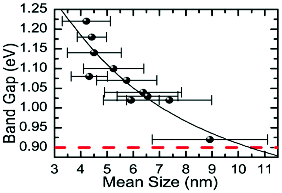 | ||
| Fig. 15 Relationship between the energy of the band gap and the mean size (diameter) for SnSe nanocrystals produced by Baumgardner et al. using thermolysis.67 Reprinted with permission from Baumgardner et al., J. Am. Chem. Soc., 2010, 132, 9519–9521. Copyright 2010 American Chemical Society. | ||
Another solution-phase synthesis of SnSe or SnSe2 nanocrystals suitable for use in solar cells was reported by Franzman et al.68 Nanocrystals were synthesised by the reaction of di-tert-butyl diselenide with tin(II) chloride in a mixture of dodecylamine and dodecanethiol at 95 °C with brief heating at 180 °C followed by cooling and precipitation by addition of ethanol. The ratio of di-tert-butyl diselenide to tin(II) chloride allowed the control of the product composition with stoichiometric ratios leading to phase pure SnSe and excess (2.0 eq. di-tert-butyl diselenide) leading to phase pure berndtite SnSe2 by p-XRD pattern analysis. SnSe nanocrystals were observed to be anisotropic by TEM, with a diameter of 19 nm but having an elongated and polydisperse length (Fig. 16). A near-stoichiometric tin-selenium ratio was confirmed by EDX. Optical measurements confirmed a blue-shifted direct band gap of around 1.7 eV compared with bulk SnSe suggesting quantum confinement with absorption across the EM spectrum up to the NIR region. Functional solar cells incorporating the SnSe nanocrystals exhibited superior power conversion efficiencies (ηp) compared to the devices fabricated without SnSe (ηp = 0.06% vs. ηp = 0.03%).
 | ||
| Fig. 16 Imaging of SnSe nanocrystals produced by the method of Franzman et al. for use in solar cells. (a) HRTEM of a single nanocrystal, (b) SAED pattern with indexing of SnS crystal planes and (c) TEM of SnSe nanocrystal ensemble.68 Reprinted with permission from Franzman et al., J. Am. Chem. Soc., 2010, 132, 4060–4061. Copyright 2010 American Chemical Society. | ||
Recently, Sharma et al. prepared tin selenide nanocrystals using diorganotin(IV) 2-pyridylselenolate single source precursors of the formula [R2Sn(2-SeC5H4N)2] where R = Me, Et or tBu.57 Thermolysis of the precursors in oleylamine furnished SnSe nanoparticles with a range of product morphologies observed by SEM – from rectangular bars to rectangular and hexagonal sheets depending on the precursor used.
4. Tin telluride
Tin telluride (SnTe) is garnering much interest due to its semiconducting properties. Bulk SnTe exhibits a direct band gap of 0.19 eV at 300 K, which lies in the mid-IR region of the electromagnetic spectrum.5 The material hence has potential application in IR detection, radiation receivers and thermoelectric devices.SnTe crystallises with the cubic rock salt structure (Fig. 17) but can undergo a structural transformation to an orthorhombic form under pressure.69 Sharma et al. have performed detailed analysis of the electronic structure and ground state properties of the SnTe using a linear combination of atomic orbitals (LCAO) approach based on density functional theory (DFT) calculations.70 The calculated Compton profiles were used to discuss the electronic properties of SnTe. Comparative studies of SnTe with GeTe have been performed to contrast the nature of bonding found within the two compounds; it was found that SnTe is less covalent and more ionic than GeTe.
 | ||
| Fig. 17 Cubic SnTe. | ||
As with other metal chalcogenides, several approaches to SnTe are known, but the frequency of such reports is far lower than for either the sulfide or selenide thin films.
4.1. Synthetic routes to tin telluride thin films and nanocrystals
Bulk SnTe has a band gap of ca. 0.19 eV (mid-IR)2 and quantum confinement leads to blue-shift of the band gap toward the near-infrared region of the electromagnetic spectrum, thus SnTe potentially has uses in biomedical imaging applications in vivo or telecommunications. However, there are currently relatively few reports of syntheses of monodisperse nanocrystals of SnTe despite its great potential.Boudjouk et al. produced cubo-octahedral SnTe from single-source precursors of the type (Ph3Sn)2Te.54 This approach was expanded later with the introduction of cyclic precursors of the type (Bn2SnTe)3 also to produce cubic SnTe.71 The homoleptic tin(II) chalcogenolate complexes Sn[TeSi(SiMe3)]2 were reported by Arnold and co-workers and are suitable as single-source precursors for the synthesis of SnTe materials.72 The pyrolysis of Sn[TeSi(SiMe3)]2 at modest temperatures (250 °C) under a nitrogen atmosphere leads to the production of SnTe with the single by-product: Te[Si(SiMe3)]2. SnTe produced in this manner was characterised by p-XRD and elemental analysis. Decomposition of the precursor in hydrocarbon solvents to the metal chalcogenide could also be elicited by thermolysis, UV irradiation or the presence of Lewis bases, in this instance one equivalent of pyridine, at even lower temperatures than the pyrolysis method. Similar silylated compounds have also been reported by Chuprakov et al. of the type [Sn{(SiMe3)2CH}2(μ-E)]2 (where E = Se or Te) (vide supra).50
Schlecht et al. reported the use of nanocrystalline tin as a template for SnTe nanocrystal growth.73 The finely divided metal, produced from the reaction of SnCl2 with Li[Et3BH], was reacted with Ph2Te2 in boiling diglyme. Cubic SnTe nanoparticles with diameters of 15–60 nm, characterised by p-XRD, were produced. Nanoparticles with ca. 15 nm diameter had star-shaped morphology whilst those of 60 nm diameter were organised in random spherical agglomerates. The diameter and morphology of the particles, was controlled by concentration, with high dilutions favouring the smaller SnTe nanostars.
Tang and co-workers describe a reductive method to SnTe nanoparticles.74 Reaction of hydrated tin(IV) chloride with potassium borohydride in ethylenediamine led to a grey powder characterised by p-XRD as cubic SnTe. TEM images revealed polydisperse crystals with diameters in the range of 30–40 nm, in agreement estimated diameters calculated from p-XRD using the Scherrer equation. XPS was used to confirm the SnTe stoichiometry. The method was not compatible with tin(II) chloride or solid anhydrous tin(IV) chloride, which led to the formation of elemental tellurium in both cases.
The first examples of monodisperse SnTe nanocrystals was reported Talapin and co-workers.75 The reaction of Sn[N(SiMe3)2], with TOP-Te in an oleylamine–octadecene mixture at 150 °C. This precursor has been used for the synthesis of both SnS30 and SnSe67 nanoparticles (vide supra), and thus the methodology represents a crucial addition to the canon of semiconductor nanocrystal synthesis. SnTe nanocrystals were characterised by p-XRD, imaged with TEM and EDX was used to confirm stoichiometry (Fig. 18). Various sizes were produced in the range 7 nm–17 nm diameter (Scherrer equation), with size distributions below 10%. The size of the crystals produced in this range could be easily controlled by adjustment of injection and growth temperatures, and the amount of oleylamine in the oleylamine–octadecene mixture. Absorption spectra of the nanoparticles produced by this method allowed estimation of the band gap energies of the as-synthesised SnTe: 0.4 eV and 0.5 eV for 14 nm and 7 nm nanocrystals respectively.
 | ||
| Fig. 18 (a), (b) TEM images of SnTe NCs capped with oleic acid. (c) Powder XRD patterns of SnTe NCs with various sizes. (d), (e) HRTEM of SnTe NCs viewed along [001] and [111] zone axes.75 Reprinted with permission from Kovalenko et al., J. Am. Chem. Soc., 2007, 129, 11354–11355. Copyright 2007 American Chemical Society. | ||
Using a tin oxide hydroxide precursor for the synthesis of tin chalcogenide nanoparticles, [Sn6O4(OH)4], Ning et al. have also outlined the synthesis of nanocrystalline SnTe nanoparticles and nanowires, the latter via oriented attachment.76 Formation of nanocrystals was initiated by injection of TOP-Te into Sn6O4(OH)4 dissolved in mixtures of either oleic acid–oleylamine or oleic acid–octylamine held at 180 °C. Nanocrystals were characterised as cubic SnTe by p-XRD, TEM and HRTEM. The diameters of highly crystalline nanocrystals produced from oleylamine-containing solutions were around 4 nm. In contrast, nanocrystals produced from octylamine-containing solutions were around 8 nm with low crystallinity. It was found that prolonged reaction times for the latter case afforded an in situ conversion of SnTe nanocrystals to rather polydisperse nanowires of around 50 nm in length and around 5 nm in diameter. The authors suggest from HRTEM images of the wires that an oriented attachment growth mechanism is responsible for the growth of the wires by the growth of (200) planes in the <100> direction. A time-course study by TEM tends to reinforce these mechanistic suggestions (Fig. 19).
 | ||
| Fig. 19 Temporal study of the oriented attachment mechanism of SnSe nanowire growth by Ning et al.76 TEM images show the nanocrystalline products from aliquots taken from a reaction at various time points over a period of 10 min. Reproduced from ref. 73 with permission from the Royal Society of Chemistry. | ||
Salavati-Niasari et al. reduced tellurium(IV) chloride with potassium borohydride in the presence of tin(II) chloride under alkaline conditions,77 the precipitates obtained were analysed by p-XRD, SEM and TEM, which confirmed the product to be SnTe nanocrystals with diameters in the range of 40–50 nm, and quasi-spherical morphologies. The same tin and tellurium containing precursors were also shown to produce SnTe nanocrystals by this approach. SnTe nanocrystals produced by this method were 30–40 nm in diameter and almost monodisperse.
Tilley and co-workers have reported a solution synthesis of SnTe nanocrystals using triethanolamine (TEA) as a stabilising agent.78 The nanoparticles are characterised by p-XRD, SAED and EDX. The reaction is said to be as a greener phosphine-free alternative to the Talapin synthesis,75 though the nanocrystals produced by this method seem to be somewhat more polydisperse. The diameter of the nanoparticles could be controlled by the amount of TEA added to the SnBr2–telluride reagent mixture, allowing access to sizes from 3 to 32 nm. Nanocrystals exhibited quantum confinement effects, with band gaps measured as 0.5 eV and 0.4 eV for nanoparticles with diameters of 6.5 nm and 14 nm respectively. The method is expected to be applicable to the production of other metal chalcogenide nanocrystals.
Schaak and co-workers recently described a rather interesting general method for the conversion of libraries of tin(II) sulfide and selenide nanosheets into telluride nanosheets by reaction with TOP-Te.79 The mechanism is believed to proceed via direct anion exchange of the chalcogenide ions, and could represent a general reaction for accessing previously inaccessible tin telluride nanostructures.
5. Synthetic routes to copper zinc tin sulfide
Copper zinc tin sulfide (Cu2ZnSnS4; CZTS) is an emergent material for solar energy conversion.80 It has a band gap of ca. 1.5 eV with a high absorption coefficient of 104 cm−1. Like tin sulfide, it is composed of non-toxic and relatively earth-abundant elements and hence is attractive for sustainable solar energy. It is an alternative material to CuInGaS2 (CIGS) in thin film solar cells as it is cheaper to produce in theory and there has recently been considerable research focused on the synthesis and growth of CZTS nanocrystals and thin films. CZTS based absorber layers processed from solution have been shown to have higher solar energy conversion efficiencies than vacuum deposited films, thus leading to the prospect of mass production from scale-up.81 Current record solar cell power conversion efficiencies from CZTS-based materials stand at ca. 11%, making the prospect of commercialisation likely.82 CZTS displays polymorphism, existing in the wurtzite kesterite, wurtzite stannite, zinc blende stannite and zinc blende kesterite forms with varying theoretical stabilities.83Ryan and co-workers used a colloidal synthesis to produce CZTS nanorods in the wurtzitic phase84 (Fig. 20). A mixture of copper(II) acetyl acetonate, zinc acetate, tin(IV) acetate and TOP oxide was mixed in octadecene and heated to 240–260 °C. At 150–160 °C a mixture of 1-dodecane thiol and tert-dodecyl mercaptan was injected into the reaction. Nanorod growth was allowed for up to 30 min, after which cooling and addition of toluene quenched the reaction. The nanoparticles were purified by centrifugation. Dark-field scanning transmission electron microscopy (DF-STEM) of the product showed nanorods of 11 nm × 35 nm dimensions. Selected area electron diffraction (SAED) revealed that the nanorods were of wurtzite phase. Optical absorbance measurements revealed a band gap of ca. 1.4 eV.
 | ||
| Fig. 20 DF-STEM and HR-TEM images of bullet-shaped CZTS nanorods produced by Ryan and co-workers.84 (a) DF-STEM image of nanorods inset: SAED pattern revealing wurtzite phase. (b) HR-TEM image of two nanorods revealing elongation in the [002] direction. Reprinted with permission from Singh et al., J. Am. Chem. Soc., 2012, 134, 2910–2913. Copyright 2012 American Chemical Society. | ||
CZTS nanocrystals have been synthesized by Khare et al. using the thermal decomposition of diethyl dithiocarbamate complexes of copper(II), zinc and tin(IV) in mixtures of oleic acid and octadecene.85 The spherical nanocrystals produced by this method had diameters of 2, 2.5, 5 or 7 nm by HRTEM depending on the decomposition conditions employed. Injection of oleylamine at 150 °C produced nanocrystals of 2 nm diameter. Injection of oleylamine and octadecene at 150 °C gave 2.5 nm nanocrystals. A higher decomposition temperature of 175 °C afforded nanocrystals with diameters of 5 and 7 nm were formed. To avoid the thermal decomposition of the tin precursor under the latter synthetic conditions, it had to be co-injected with oleylamine and octadecene. An increase in the band gap from 1.5 eV to 1.8 eV with decreasing particle radius was determined from optical absorbance measurements thus demonstrating quantum confinement. Similarly, Han and co-workers have reported the synthesis of CZTS nanocrystals in the wurtzite phase from the decomposition of copper(II) and zinc(II) diethyldithiocarbamate complexes along with tin(IV) diethyl dithiocarbamate.86 Heating of the complexes at 250 °C for 30 min in a hexadecanethiol–trioctylamine mixture afforded monodisperse bullet-shaped nanorods of dimensions 15.1 ± 1 nm × 7.6 ± 0.6 nm characterised by TEM, EDX, XPS and p-XRD. Trimmel and co-workers have developed routes towards CZTS films from the decomposition of copper(I), tin(IV) and zinc xanthate precursors. Solar cells incorporating close-to stoichiometric CZTS from this method have an efficiency of 0.1% with a band gap of 1.3 eV.87
Jiang et al. isolated metastable Cu2ZnSnS4 nanocrystals with an orthorhombic phase.88 using the reaction of CuCl2, ZnCl2, SnCl2 and thiocarbamide at 200 °C for 24 h. The as-synthesised nanocrystals had plate-like morphology with size varying from 20 to 50 nm. It was reported that the metastable orthorhombic phase can be transformed to stable kesterite phase by annealing at 500 °C.
Cabot and co-workers have demonstrated that continuous-flow processing may be a viable method for the production of CZTS nanocrystals.89 Precursor solutions containing copper(II) chloride, tin(IV) chloride and zinc oxide in mixtures of oleylamine and octadecene were flowed through a 1 m × 3 mm tube in diameter at a rate of 1–5 mL min−1. Heating in situ to 300–320 °C caused decomposition of the precursor solution, affording nanocrystals of CZTS of various sizes, shapes and compositions depending on the specific reaction conditions.
Prieto and co-workers used thermal decomposition of a mixture copper(II) acetylacetonate, zinc acetate, and tin(II) acetate, and a mixture of sulfur–selenium with sodium borohydride in oleylamine and trioctylphosphine oxide (TOPO) to afford Cu2ZnSn(S1−xSex)4 nanocrystals with tunable selenium–sulfur composition.90 Band gap of the nanocrystals decreased from 1.54 eV to 1.47 eV as selenium replaced sulfur in the CZTS nanocrystals. Similarly, Ou et al. used a hot injection of copper, zinc and tin stearate complexes in oleylamine into thiourea and selenium in octadecene at 270 °C to produce Cu2ZnSn(SxSe1−x)4 nanocrystals. Optical band gaps ranging from 1.5 eV to 1.0 eV were observed, the energy decreasing as the amount of selenium increased.
Sol–gel processing of CZTS nanowires and nanotubes using an anodized alumina (AAO) template with 200 nm pore size has been reported by Su et al.91 The CZTS sol–gel was prepared by dissolving copper(II) acetate, zinc(II) acetate and tin(II) chloride in 2-methoxyethanol. Immersion of the AAO templates into the precursor solution followed by annealing at 550 °C under a sulfurous atmosphere and etching with sodium hydroxide afforded the immobilised nanowire/nanotube array. CZTS nanowires and nanotubes of dimensions 200 nm × 60 μm were produced, the width dictated by the AAO template. Optical band gaps of 1.57 eV and 1.61 eV were measured for nanowires and nanotubes respectively.
There has been further research into solar cell device fabrication using solution-processed CZTS. CZTS solar cells with 1.9% solar energy conversion efficiency, 0.484 V open-circuit voltage, 8.91 mA cm−2 short-circuit current density and a 45% fill factor have been reported by Hu and co-workers.92 CZTS nanocrystals use to fabricate the cell were synthesized by the reaction of copper(II) and tin(II) chloride and zinc sulfate with Na2S in ethylene glycol solution heated at 180 °C for 12 hours. Pal and co-workers prepared a CZTS-fullerene pn-junction hybrid solar cell with power conversion efficiency of 0.9% and a fill factor of 43%.93 CZTS nanocrystals were synthesised by the reaction of tin(IV) chloride, copper(II) chloride and zinc chloride with sulfur in oleylamine at 180 °C. Nanoparticles were spin-coated on an ITO substrate and then coated with a layer of the fullerene [6,6]-phenyl-C61-butyric acid methyl ester (PCBM) to form the pn-junction.
O'Brien and co-workers presented the first report of CZTS thin films deposited by a chemical vapour deposition approach from discrete molecular precursors. Compatible precursors based on simple metal diethyldithiocarbamate complexes of formula [M(S2CNEt2)] (where M = Cu2+, Zn2+) and diorganotin complexes of the type [Sn(Bu)2(S2CNEt2)2] were mixed in the correct 2Cu:1Zn:1Sn stoichiometry and AACVD performed from toluene solutions at various furnace temperatures. p-XRD was used to confirm the phase of deposited Cu2ZnSnS as either kesterite or stannite. SEM showed granular crystallites with sizes dependent on temperature. EDX was used to confirm the correct stoichiometry of the thin films deposited at 360 °C. EDX elemental mapping demonstrated the even distribution of Cu, Zn, Sn and S across the entire substrate (Fig. 21).
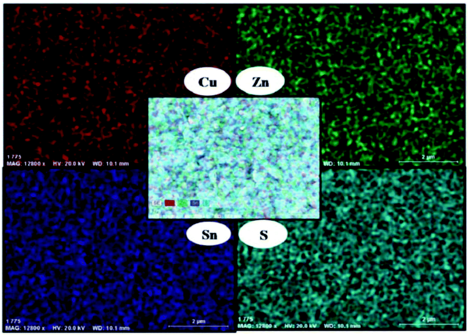 | ||
| Fig. 21 EDX elemental mapping of CZTS thin films produced by O'Brien and co-workers by using AACVD with a mix of three discrete molecular precursors.94 Reproduced from ref. 94 with permission from The Royal Society of Chemistry. | ||
6. Synthetic routes to mesostructured tin chalcogenide materials
Mesostructured compounds are a hugely important class of condensed phase materials which contain regular repeating motifs to produce three-dimensional ordering of the material which leads to higher ordering in the crystalline material e.g. formation of pores of defined size and shape. Pore sizes in mesoporous materials lie between those of microporous materials (<2 nm) and macroporous solids (>50 nm).95 Traditionally these materials have been based on alumina, silica or aluminosilicate superstructures with popular examples such as zeolites, molecular sieves and mesoporous silica finding use in catalysis, ion exchange, drying of solvents and optoelectronic applications. Recently, however, there has been a paradigm shift with non-oxide inorganic materials used to produce novel mesostructured compounds.96 The synthesis, structural, spectroscopic and sorption properties of microporous tin chalcogenides have been reported,97–100 but more recently, reports of novel syntheses of mesostructured materials have appeared.Ozin and co-workers described the synthesis of a novel class of tin(IV) sulfide thermotropic liquid crystals.101 Reaction of tin(IV) chloride with ammonium sulfide and hexadecylamine (HDA) in the aqueous alkaline media formed a light yellow gel which was crystallised at 150 °C over 19 hours to form an intriguing yellow monolith of formula SnS2.07(HDA)2.34(H2O)2.23 by elemental analysis with a large d-spacing of 5.1 nm by p-XRD. Further washing with excess acetone afforded material with reduced d-spacing. p-XRD, SEM and TEM revealed a mesoporous structure consisting of stacked two-dimensional layers of hexagonal SnS2 with a fully-extended hexadecylamine bilayer in the inter-lamellar space. Solid-state magic angle spinning NMR of the 119Sn metallo-centres revealed two tin coordination environments: 5- and 6-coordinate. Raman spectroscopy revealed a new band implying a changed bond distance consistent with a lower coordination than 6. The UV-Vis absorption spectrum revealed an absorption edge lying between that of five-coordinate and six-coordinate tin species. Thermal behaviour was studied by TGA and DSC and variable-temperature p-XRD, with crystalline (RT – 45 °C), semi-liquid (45 °C–85 °C) and liquid crystalline (>85 °C) phases identified. The material is electrically conducting, especially so in the liquid crystalline phase compared to the other phases, and can reversibly adsorb water and carbon dioxide, thus heralding the material as having use in optoelectronic and sensing applications. The lamellae were later imaged by tapping-mode AFM, with parallel stacked layers in the z-direction observed with an inter-lamellar distance of 5 nm. Imaging in the x, y plane by two-dimensional fast Fourier transform-AFM revealed a periodic arrangement of mesopores with sizes in the range of 3–10 nm.102 Similarly, Rao and Neeraj reported mesostructured SnS2 composites produced by the reaction of tin(IV) chloride with sodium sulfide in the presence of dodecylamine surfactant.103 The composites displayed a lamellar structure with a periodic interlamellar spacing of 3.12 nm as measured by p-XRD. Kessler and co-workers produced mesostructured tin(IV) sulfide by the reaction of sodium sulfide and tin(IV) chloride in the presence of cetyl trimethyl ammonium bromide surfactant under alkaline conditions.104 The reaction produced lamellar mesostructured tin(IV) sulfide with spacing between layers of around 2.6 nm. The reaction can be translated to produce a number of materials with differences in long and short range order throughout the material.105 Indeed, tin coordination geometry can be varied between octahedral and tetrahedral by variation of surfactant amount. Transformation between various lamellar phases has been described.106
Solution phase co-assembly of zintl clusters of the type SnE44− (where E = Se, Te) have been exploited by the groups of Tolbert and Kanatzidis to prepare a range of mesostructured tin chalcogenides. This novel approach relies on the templating of the zintl clusters by surfactant molecules, either with or without the presence of transition metal cations. Initially, assembly of the zintl clusters using square-planar platinum(II) ions was presented,107 giving rise to platinum tin telluride mesostructured composites, with periodic mesostructure as-imaged by TEM. EXAFS was used to demonstrate the structure consisting of a square planar d8 platinum(II) centres bonded to four Sn2Te6 clusters (Fig. 22), with reduction of the platinum(IV) starting material presumably occurring during reaction. This approach, draws parallels with supramolecular chemistry; the development of metal templated structures by Lehn,108 for instance, being especially salient to the principles used here, where the ligand field preferences of a metal cation dictates the structure of the final assembly. Riley and Tolbert cite the work of Ozin which states that square planar geometry of the linking metal cation in Ge4S10 systems is crucial to the formation of mesophases.109 The narrow band gap of 0.8 eV is potentially useful in optoelectronic applications.
 | ||
| Fig. 22 Platinum tin telluride structure deduced by Riley and Tolbert from EXAFS data.107 | ||
Korlann et al. later reported the use of cross-linking with either Pt(II) or Pt(IV) salts in varying ratios to perturb the electronic structure of the composites and modulate properties.110 A range of different transition metals ions (Ni2+, Pt2+, Zn2+) have been investigated for the templating of the zintl ions SnSe44− and SnTe44−.111 Composites produced had wormlike morphology. Rhodium gave tin telluride materials with hexagonal honeycombed (P6mm) habit. Platinum combined with SnSe44− gave materials with cubic (la3d) architecture. The SnTe44− alone, with no metal ions, gave lamellar structures. Thus, the morphology of the materials is easily controllable by judicious choice of metal ion. Recent work has focused on tuning the band gap of these materials with even greater precision.112
Hexagonally ordered mesostructured ternary metal tin sulfide materials have been reported by Kanatzidis and co-workers.113 New mesophases designated as (CP)xMySn2S6 (where M = Zn2+, Cd2+, Ga3+) were synthesized by linking Sn2S64− clusters with metal ions in the presence of cetylpyridinium (CP) surfactant molecules in formamide solution under basic conditions. The materials are semiconductors in the with band gaps in the energy range 2.5–3.1 eV. Additionally, (CP)xMySn2S6 exhibits photoluminescence when irradiated with light of energies larger than the band gap.
7. Conclusions
Research into synthetic routes for tin chalcogenides is currently flourishing due to a need for efficient and tuneable materials in various applications. The inherent band gap of many of the tin chalcogenides is commensurate with many current ubiquitous and useful semiconductor materials. Quantum confinement effects allow tuning of band gap energies by changing the size of the nanocrystal allowing the formation of tailor-made materials for any given application e.g. photovoltaics. Relatively newer alloyed materials such as the copper zinc tin sulfides (CZTS) are providing new opportunities for materials research especially for solar energy applications. The move to nanoscale materials from thin films is essential for tuning the semiconductor properties. A mastery of thin film deposition in this area, which arguably does not exist at the moment, will be the key to the further development of novel nanoscale CZT-chalcogenide materials. Exciting new mesostructured composite materials are being made with novel syntheses, often based on templating by cluster compounds. This area of research will grow ever more important as the search for more efficient, environmentally benign and cheaper semiconducting materials continues.References
- H. Xuebo and Z. Jing, in Nanofabrication and its Application in Renewable Energy, Royal Society of Chemistry, Cambridge, 2014, pp. 199–215 Search PubMed.
- P. Sinsermsuksakul, L. Sun, S. W. Lee, H. H. Park, S. B. Kim, C. Yang and R. G. Gordon, Adv. Energy Mater., 2014 DOI:10.1002/aenm.201400496.
- J. J. Loferski, J. Appl. Phys., 1956, 27, 777–784 Search PubMed.
- T. Jiang and G. A. Ozin, J. Mater. Chem., 1998, 8, 1099–1108 RSC.
- O. Madelung, Semiconductors – Basic Data, Springer-Verlag, Berlin, 2nd edn, 1996 Search PubMed.
- S. C. Ray, M. K. Karanjai and D. DasGupta, Thin Solid Films, 1999, 350, 72–78 Search PubMed.
- A. Abou Shama and H. M. Zeyada, Opt. Mater., 2003, 24, 555–561 CrossRef CAS.
- M. Ristov, G. Sinadinovski, I. Grozdanov and M. Mitreski, Thin Solid Films, 1989, 173, 53–58 CrossRef CAS.
- P. K. Nair, M. T. S. Nair and J. Campos, J. Electrochem. Soc., 1993, 140, 539–541 Search PubMed.
- R. D. Engelken, H. E. McCloud, C. Lee, M. Slayton and H. Ghoreishi, J. Electrochem. Soc., 1987, 134, 2696–2707 CrossRef CAS PubMed.
- A. Tanusevski, Semicond. Sci. Technol., 2003, 18, 501–505 Search PubMed.
- C. Gao and H. Shen, Thin Solid Films, 2012, 520, 3523–3527 CrossRef CAS PubMed.
- S. K. Arora, D. H. Patel and M. K. Agarwal, J. Cryst. Growth, 1993, 131, 268–270 CrossRef CAS.
- S. K. Arora, D. H. Patel and M. K. Agarwal, J. Mater. Sci., 1994, 29, 3979–3983 CrossRef CAS.
- P. Sinsermsuksakul, J. Heo, W. Noh, A. S. Hock and R. G. Gordon, Adv. Energy Mater., 2011, 1, 1116–1125 CrossRef CAS PubMed.
- M. Calixto-Rodriguez, H. Martinez, A. Sanchez-Juarez, J. Campos-Alvarez, A. Tiburcio-Silver and M. E. Calixto, Thin Solid Films, 2009, 517, 2497–2499 CrossRef CAS PubMed.
- E. Schonherr and W. Stetter, J. Cryst. Growth, 1975, 30, 96–98 CrossRef.
- B. P. Bade, S. S. Garje, Y. S. Niwate, M. Afzaal and P. O'Brien, Chem. Vap. Deposition, 2008, 14, 292–295 CrossRef CAS PubMed.
- T. G. Hibbert, M. F. Mahon, K. C. Molloy, L. S. Price and I. P. Parkin, J. Mater. Chem., 2001, 11, 469–473 RSC.
- L. S. Price, I. P. Parkin, T. G. Hibbert and K. C. Molloy, Chem. Vap. Deposition, 1998, 4, 222–225 CAS.
- A. Sanchez-Juarez, A. Tiburcio-Silver and A. Ortiz, Thin Solid Films, 2005, 480–481, 452–456 CrossRef CAS PubMed.
- M. Lazell, P. O'Brien, D. J. Otway and J. H. Park, J. Chem. Soc., Dalton Trans., 2000, 4479–4486 Search PubMed.
- M. A. Malik, M. Afzaal and P. O'Brien, Chem. Rev., 2010, 110, 4417–4446 Search PubMed.
- G. Barone, T. G. Hibbert, M. F. Mahon, K. C. Molloy, L. S. Price, I. P. Parkin, A. M. E. Hardy and M. N. Field, J. Mater. Chem., 2001, 11, 464–468 RSC.
- I. P. Parkin, L. S. Price, T. G. Hibbert and K. C. Molloy, J. Mater. Chem., 2001, 11, 1486–1490 RSC.
- A. T. Kana, T. G. Hibbert, M. F. Mahon, K. C. Molloy, I. P. Parkin and L. S. Price, Polyhedron, 2001, 20, 2989–2995 CrossRef CAS.
- K. Ramasamy, V. L. Kuznetsov, K. Gopal, M. A. Malik, J. Raftery, P. P. Edwards and P. O'Brien, Chem. Mater., 2013, 25, 266–276 CrossRef CAS.
- H. L. Zhu, D. R. Yang, Y. J. Ji, H. Zhang and X. F. Shen, J. Mater. Sci., 2005, 40, 591–595 Search PubMed.
- C. An, K. Tang, G. Shen, C. Wang, Q. Yang, B. Hai and Y. Qian, J. Cryst. Growth, 2002, 244, 333–338 Search PubMed.
- S. G. Hickey, C. Waurisch, B. Rellinghaus and A. Eychmüller, J. Am. Chem. Soc., 2008, 130, 14978–14980 CrossRef CAS PubMed.
- Y. K. Liu, D. D. Hou and G. H. Wang, Chem. Phys. Lett., 2003, 379, 67–73 CrossRef CAS PubMed.
- G. Z. Shen, D. Chen, K. B. Tang, L. Y. Huang, Y. T. Qian and G. Zhou, Inorg. Chem. Commun., 2003, 6, 178–180 CrossRef CAS.
- A. J. Biacchi, D. D. Vaughn and R. E. Schaak, J. Am. Chem. Soc., 2013, 135, 11634–11644 CrossRef CAS PubMed.
- H. Liu, Y. Liu, Z. Wang and P. He, Nanotechnology, 2010, 21, 105707 CrossRef PubMed.
- Y. Xu, N. Al-Salim, C. W. Bumby and R. D. Tilley, J. Am. Chem. Soc., 2009, 131, 15990 Search PubMed.
- S. Sohila, M. Rajalakshmi, C. Muthamizhchelvan, S. Kalavathi, C. Ghosh, R. Divakar, C. N. Venkiteswaran, N. G. Muralidharan, A. K. Arora and E. Mohandas, Mater. Lett., 2011, 65, 1148–1150 Search PubMed.
- S. Sohila, M. Rajalakshmi, C. Ghosh, A. K. Arora and C. Muthamizhchelvan, J. Alloys Compd., 2011, 509, 5843–5847 CrossRef CAS PubMed.
- Y. Zhang, J. Lu, S. Shen, H. Xu and Q. Wang, Chem. Commun., 2011, 47, 5226–5228 RSC.
- Q. Han, M. Wang, J. Zhu, X. Wu, L. Lu and X. Wang, J. Alloys Compd., 2011, 509, 2180–2185 CrossRef CAS PubMed.
- J. Ning, K. Men, G. Xiao, L. Wang, Q. Dai, B. Zou, B. Liu and G. Zou, Nanoscale, 2010, 2, 1699–1703 Search PubMed.
- M. Yousefi, M. Salavati-Niasari, F. Gholamian, D. Ghanbari and A. Aminifazl, Inorg. Chim. Acta, 2011, 371, 1–5 Search PubMed.
- D. D. Vaughn II, O. D. Hentz, S. Chen, D. Wang and R. E. Schaak, Chem. Commun., 2012, 48, 5608–5610 Search PubMed.
- B. K. Patra, S. Sarkar, A. K. Guria and N. Pradhan, J. Phys. Chem. Lett., 2013, 4, 3929–3934 Search PubMed.
- E. C. Greyson, J. E. Barton and T. W. Odom, Small, 2006, 2, 368–371 CrossRef CAS PubMed.
- Z. T. Deng, D. R. Han and Y. Liu, Nanoscale, 2011, 3, 4346–4351 RSC.
- L. Ren, Z. Jin, W. Wang, H. Liu, J. Lai, J. Yang and Z. Hong, Appl. Surf. Sci., 2011, 258, 1353–1358 CrossRef CAS PubMed.
- I. Lefebvre, M. A. Szymanski, J. Olivier-Fourcade and J. C. Jumas, Phys. Rev. B: Condens. Matter, 1998, 58, 1896–1906 CrossRef CAS.
- J. P. Singh and R. K. Bedi, Thin Solid Films, 1991, 199, 9–12 CrossRef CAS.
- K. J. John, B. Pradeep and E. Mathai, J. Mater. Sci., 1994, 29, 1581–1583 Search PubMed.
- I. S. Chuprakov, K. H. Dahmen, J. J. Schneider and J. Hagen, Chem. Mater., 1998, 10, 3467–3470 Search PubMed.
- N. D. Boscher, C. J. Carmalt, R. G. Palgrave and I. P. Parkin, Thin Solid Films, 2008, 516, 4750–4757 CrossRef CAS PubMed.
- R. Indirajith, T. P. Srinivasan, K. Ramamurthi and R. Gopalakrishnan, Curr. Appl. Phys., 2010, 10, 1402–1406 Search PubMed.
- S. R. Bahr, P. Boudjouk and G. J. McCarthy, Chem. Mater., 1992, 4, 383–388 CrossRef CAS.
- P. Boudjouk, D. J. Seidler, S. R. Bahr and G. J. McCarthy, Chem. Mater., 1994, 6, 2108–2112 CrossRef CAS.
- P. Boudjouk, D. J. Seidler, D. Grier and G. J. McCarthy, Chem. Mater., 1996, 8, 1189–1196 Search PubMed.
- Y. Cheng, T. J. Emge and J. G. Brennan, Inorg. Chem., 1996, 35, 342–346 CrossRef CAS PubMed.
- R. K. Sharma, G. Kedarnath, A. Wadawale, C. A. Betty, B. Vishwanadh and V. K. Jain, Dalton Trans., 2012, 41, 12129–12138 RSC.
- N. Kumar, V. Sharma, U. Parihar, R. Sachdeva, N. Padha and C. J. Panchal, J. Nano- Electron. Phys., 2011, 3, 117–126 Search PubMed.
- C. Wang, Y. D. Li, G. H. Zhang, J. Zhuang and G. Q. Shen, Inorg. Chem., 2000, 39, 4237–4239 CrossRef CAS.
- B. Pejova and I. Grozdanov, Thin Solid Films, 2007, 515, 5203–5211 CrossRef CAS PubMed.
- B. Pejova and A. Tanusevski, J. Phys. Chem. C, 2008, 112, 3525–3537 CAS.
- D. D. Vaughn II, S.-I. In and R. E. Schaak, ACS Nano, 2011, 5, 8852–8860 CrossRef PubMed.
- S. Liu, X. Guo, M. Li, W.-H. Zhang, X. Liu and C. Li, Angew. Chem., Int. Ed., 2011, 50, 12050–12053 CrossRef CAS PubMed.
- M. Achimovicova, A. Recnik, M. Fabian and P. Balaz, Acta Montan. Slovaca, 2011, 16, 123–127 Search PubMed.
- M. Achimovicova, K. L. da Silva, N. Daneu, A. Recnik, S. Indris, H. Hain, M. Scheuermann, H. Hahn and V. Sepelak, J. Mater. Chem., 2011, 21, 5873–5876 RSC.
- X. Yu, J. Zhu, Y. Zhang, J. Weng, L. Hu and S. Dai, Chem. Commun., 2012, 48, 3324–3326 RSC.
- W. J. Baumgardner, J. J. Choi, Y.-F. Lim and T. Hanrath, J. Am. Chem. Soc., 2010, 132, 9519–9521 Search PubMed.
- M. A. Franzman, C. W. Schlenker, M. E. Thompson and R. L. Brutchey, J. Am. Chem. Soc., 2010, 132, 4060–4061 CrossRef CAS PubMed.
- T. Chattopadhyay, H. G. Vonschnering, W. A. Grosshans and W. B. Holzapfel, Physica B+C, 1986, 139, 356–360 CrossRef.
- G. Sharma, P. Bhambhani, N. Munjal, V. Sharma and B. K. Sharma, J. Nano- Electron. Phys., 2011, 3, 341–347 Search PubMed.
- P. Boudjouk, M. P. Remington, D. G. Grier, W. Triebold and B. R. Jarabek, Organometallics, 1999, 18, 4534–4537 Search PubMed.
- A. L. Seligson and J. Arnold, J. Am. Chem. Soc., 1993, 115, 8214–8220 CrossRef CAS.
- S. Schlecht, M. Budde and L. Kienle, Inorg. Chem., 2002, 41, 6001–6005 CrossRef CAS PubMed.
- C. An, K. Tang, B. Hai, G. Shen, C. Wang and Y. Qian, Inorg. Chem. Commun., 2003, 6, 181–184 Search PubMed.
- M. V. Kovalenko, W. Heiss, E. V. Shevchenko, J.-S. Lee, H. Schwinghammer, A. P. Alivisatos and D. V. Talapin, J. Am. Chem. Soc., 2007, 129, 11354–11355 CrossRef CAS PubMed.
- J. Ning, K. Men, G. Xiao, B. Zou, L. Wang, Q. Dai, B. Liu and G. Zou, CrystEngComm, 2010, 12, 4275–4279 RSC.
- M. Salavati-Niasari, M. Bazarganipour, F. Davar and A. A. Fazl, Appl. Surf. Sci., 2010, 257, 781–785 CrossRef CAS PubMed.
- Y. Xu, N. Al-Salim, J. M. Hodgkiss and R. D. Tilley, Cryst. Growth Des., 2011, 11, 2721–2723 CAS.
- I. T. Sines, D. D. Vaughn II, A. J. Biacchi, C. E. Kingsley, E. J. Popczun and R. E. Schaak, Chem. Mater., 2012, 24, 3088–3093 CrossRef CAS.
- K. Ramasamy, M. A. Malik and P. O'Brien, Chem. Commun., 2012, 48, 5703–5714 Search PubMed.
- D. A. R. Barkhouse, O. Gunawan, T. Gokmen, T. K. Todorov and D. B. Mitzi, Prog. Photovoltaics, 2012, 20, 6–11 CAS.
- T. K. Todorov, J. Tang, S. Bag, O. Gunawan, T. Gokmen, Y. Zhu and D. B. Mitzi, Adv. Energy Mater., 2013, 3, 34–38 CrossRef CAS PubMed.
- S. Chen, A. Walsh, Y. Luo, J. H. Yang, X. G. Gong and S. H. Wei, Phys. Rev. B: Condens. Matter, 2010, 82, 195203 CrossRef.
- A. Singh, H. Geaney, F. Laffir and K. M. Ryan, J. Am. Chem. Soc., 2012, 134, 2910–2913 CrossRef CAS PubMed.
- A. Khare, A. W. Wills, L. M. Ammerman, D. J. Norris and E. S. Aydil, Chem. Commun., 2011, 47, 11721–11723 Search PubMed.
- M. D. Regulacio, C. Ye, S. H. Lim, M. Bosman, E. Ye, S. Chen, Q.-H. Xu and M.-Y. Han, Chem. – Eur. J., 2012, 18, 3127–3131 CrossRef CAS PubMed.
- A. Fischereder, A. Schenk, T. Rath, W. Haas, S. Delbos, C. Gougaud, N. Naghavi, A. Pateter, R. Saf, D. Schenk, M. Edler, K. Bohnemann, A. Reichmann, B. Chernev, F. Hofer and G. Trimmel, Monatsh. Chem., 2013, 144, 273–283 Search PubMed.
- H. Jiang, P. Dai, Z. Feng, W. Fan and J. Zhan, J. Mater. Chem., 2012, 22, 7502–7506 Search PubMed.
- A. Shavel, D. Cadavid, M. Ibanez, A. Carrete and A. Cabot, J. Am. Chem. Soc., 2012, 134, 1438–1441 CrossRef CAS PubMed.
- S. C. Riha, B. A. Parkinson and A. L. Prieto, J. Am. Chem. Soc., 2011, 133, 15272–15275 CrossRef CAS PubMed.
- Z. Su, C. Yan, D. Tang, K. Sun, Z. Han, F. Liu, Y. Lai, J. Li and Y. Liu, CrystEngComm, 2012, 14, 782–785 RSC.
- Q. Tian, X. Xu, L. Han, M. Tang, R. Zou, Z. Chen, M. Yu, J. Yang and J. Hu, CrystEngComm, 2012, 14, 3847–3850 RSC.
- S. K. Saha, A. Guchhait and A. J. Pal, Phys. Chem. Chem. Phys., 2012, 14, 8090–8096 Search PubMed.
- K. Ramasamy, M. A. Malik and P. O'Brien, Chem. Sci., 2011, 2, 1170–1172 RSC.
- J. Rouquerol, D. Avnir, C. W. Fairbridge, D. H. Everett, J. H. Haynes, N. Pernicone, J. D. F. Ramsay, K. S. W. Sing and K. K. Unger, Pure Appl. Chem., 1994, 66, 1739–1758 CrossRef CAS.
- M. G. Kanatzidis, Adv. Mater., 2007, 19, 1165–1181 Search PubMed.
- T. Jiang, A. Lough, G. A. Ozin and R. L. Bedard, J. Mater. Chem., 1998, 8, 733–741 Search PubMed.
- T. Jiang, A. Lough, G. A. Ozin, R. L. Bedard and R. Broach, J. Mater. Chem., 1998, 8, 721–732 RSC.
- T. Jiang, G. A. Ozin and R. L. Bedard, J. Mater. Chem., 1998, 8, 1641–1648 RSC.
- T. Jiang, G. A. Ozin, A. Verma and R. L. Bedard, J. Mater. Chem., 1998, 8, 1649–1656 RSC.
- T. Jiang and G. A. Ozin, J. Mater. Chem., 1997, 7, 2213–2222 RSC.
- I. Sokolov, T. Jiang and G. A. Ozin, Adv. Mater., 1998, 10, 942–946 CrossRef CAS.
- Neeraj and C. N. R. Rao, J. Mater. Chem., 1998, 8, 279–280 RSC.
- J. Li, L. Delmotte and H. Kessler, Chem. Commun., 1996, 1023–1024 Search PubMed.
- J. Q. Li, H. Kessler and L. Delmotte, J. Chem. Soc., Faraday Trans., 1997, 93, 665–668 Search PubMed.
- J. Q. Li and H. Kessler, Microporous Mater., 1997, 9, 141–147 CrossRef CAS.
- A. E. Riley and S. H. Tolbert, J. Am. Chem. Soc., 2003, 125, 4551–4559 CrossRef CAS PubMed.
- B. Hasenknopf, J.-M. Lehn, B. O. Kneisel, G. Baum and D. Fenske, Angew. Chem., Int. Ed. Engl., 1996, 35, 1838–1840 CrossRef CAS PubMed.
- M. J. MacLachan, N. Coombs and G. A. Ozin, Nature, 1999, 397, 681 Search PubMed.
- S. D. Korlann, A. E. Riley, B. L. Kirsch, B. S. Mun and S. H. Tolbert, J. Am. Chem. Soc., 2005, 127, 12516–12527 Search PubMed.
- A. E. Riley, S. D. Korlann, E. K. Richman and S. H. Tolbert, Angew. Chem., Int. Ed., 2006, 45, 235–241 CrossRef CAS PubMed.
- S. D. Korlann, A. E. Riley, B. S. Mun and S. H. Tolbert, J. Phys. Chem. C, 2009, 113, 7697–7705 CAS.
- K. K. Rangan, P. N. Trikalitis, C. Canlas, T. Bakas, D. P. Weliky and M. G. Kanatzidis, Nano Lett., 2002, 2, 513–517 Search PubMed.
| This journal is © the Partner Organisations 2014 |