Themed collection 2D Materials

Themed issue on 2D materials
Guest editors Manish Chhowalla, Zhong Lin and Mauricio Terrones introduce this Journal of Materials Chemistry C themed issue on 2D materials.

J. Mater. Chem. C, 2017,5, 11156-11157
https://doi.org/10.1039/C7TC90171B
Emerging two-dimensional halide perovskite nanomaterials
This article highlights recent developments of an emerging family of nanomaterials: two-dimensional halide perovskites.

J. Mater. Chem. C, 2017,5, 11165-11173
https://doi.org/10.1039/C7TC02863F
Combining 2D inorganic semiconductors and organic polymers at the frontier of the hard–soft materials interface
Recent advances in combining functional organic polymers with inorganic 2D semiconductors for nanoscale electronics are highlighted.

J. Mater. Chem. C, 2017,5, 11158-11164
https://doi.org/10.1039/C7TC02790G
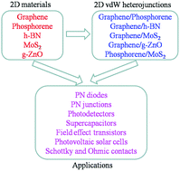
Two-dimensional van der Waals heterojunctions for functional materials and devices
Two-dimensional (2D) van der Waals heterojunctions combining the electronic structures of such 2D materials have been predicted theoretically and synthesized experimentally to expect more new properties and potential applications far beyond corresponding 2D materials.
J. Mater. Chem. C, 2017,5, 12289-12297
https://doi.org/10.1039/C7TC04697A
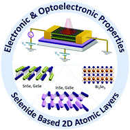
Recent advances in investigations of the electronic and optoelectronic properties of group III, IV, and V selenide based binary layered compounds
This review article presents a comprehensive update on the recent research trends, advancement and future outlook of selected layered selenide based binary compounds featuring elements from group III, IV, and V of the periodic table.
J. Mater. Chem. C, 2017,5, 11214-11225
https://doi.org/10.1039/C7TC02866K
Electrons on the surface of 2D materials: from layered electrides to 2D electrenes
We review layered and ultrathin electrides with exciting properties like high electrical mobility, high carrier concentrations, and low work functions.

J. Mater. Chem. C, 2017,5, 11196-11213
https://doi.org/10.1039/C7TC02488F
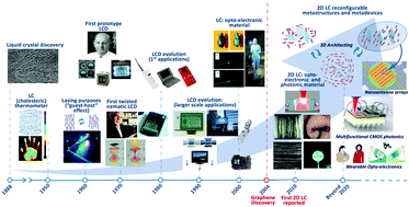
2D material liquid crystals for optoelectronics and photonics
The merging of the materials science paradigms of liquid crystals and 2D materials promises superb new opportunities for the advancement of the fields of optoelectronics and photonics. In this review, we summarise the development and applications of 2D material liquid crystals for optoelectronics and photonics.
J. Mater. Chem. C, 2017,5, 11185-11195
https://doi.org/10.1039/C7TC02549A
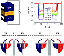
Electron spin dynamics in vertical magnetic junctions incorporating two-dimensional layered materials
The incorporation of graphene, TMDCs, insulating hBN and their hybrid systems in magnetic junctions have revealed fascinating features for spintronic devices.
J. Mater. Chem. C, 2017,5, 11174-11184
https://doi.org/10.1039/C7TC01933E
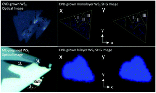
A comprehensive comparison study on the vibrational and optical properties of CVD-grown and mechanically exfoliated few-layered WS2
Tungsten disulfide (WS2), a typical transition metal dichalcogenide (TMDC) material, transits from an indirect to direct bandgap when the thickness is thinned to a monolayer, thereby allowing for applications in transistors, photodetectors, and electroluminescent devices.
J. Mater. Chem. C, 2017,5, 11239-11245
https://doi.org/10.1039/C7TC02831H
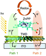
Tailoring photoelectrochemical properties of semiconducting transition metal dichalcogenide nanolayers with porphyrin functionalization
We report a facile interfacial engineering method that can drastically modulate the photoelectrochemical properties of two-dimensional transition metal dichalcogenide (TMD) semiconductors.
J. Mater. Chem. C, 2017,5, 11233-11238
https://doi.org/10.1039/C7TC02861J
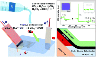
A sustainable approach to large area transfer of graphene and recycling of the copper substrate
A carbonic acid electrolyte enables sustainable, clean, rinse-free, uniform large area electrochemical delamination transfer of graphene and recycling of the copper substrate.
J. Mater. Chem. C, 2017,5, 11226-11232
https://doi.org/10.1039/C7TC02487H
Solution synthesis of few-layer WTe2 and MoxW1−xTe2 nanostructures
Colloidal nanostructures of WTe2 and MoxW1−xTe2 alloys were synthesized and characterized; multiple stacking motifs co-exist in WTe2, and the crystal structure can be tuned as a function of composition in MoxW1−xTe2.

J. Mater. Chem. C, 2017,5, 11317-11323
https://doi.org/10.1039/C7TC02860A
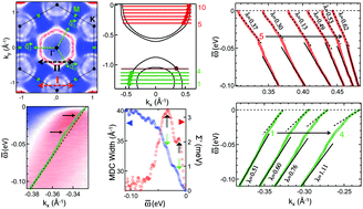
Spectroscopic signature of moment-dependent electron–phonon coupling in 2H-TaS2
An ARPES study of 2H-TaS2 reveals that its CDW transition is driven by strong electron–phonon coupling along with its momentum anisotropy.
J. Mater. Chem. C, 2017,5, 11310-11316
https://doi.org/10.1039/C7TC02641B
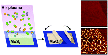
Formation of MoO3 and WO3 nanoscrolls from MoS2 and WS2 with atmospheric air plasma
Transition metal oxides in nanoscroll geometries are synthesized from two-dimensional layered precursors by plasma treatment.
J. Mater. Chem. C, 2017,5, 11301-11309
https://doi.org/10.1039/C7TC02867A
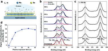
Hydrogenation of monolayer molybdenum diselenide via hydrogen plasma treatment
We report a simple and effective method for hydrogenation of monolayer MoSe2 using hydrogen plasma treatment.
J. Mater. Chem. C, 2017,5, 11294-11300
https://doi.org/10.1039/C7TC02592K
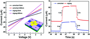
Anisotropic photoresponse of layered 2D SnS-based near infrared photodetectors
In this work, the anisotropic photoresponse and the effects of defects on the anisotropic response based on layered SnS near infrared photodetectors were investigated.
J. Mater. Chem. C, 2017,5, 11288-11293
https://doi.org/10.1039/C7TC02865B
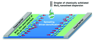
Langmuir films and uniform, large area, transparent coatings of chemically exfoliated MoS2 single layers
A simple method to create large area monolayers and multi-layer films of chemically exfoliated MoS2 is presented.
J. Mater. Chem. C, 2017,5, 11275-11287
https://doi.org/10.1039/C7TC02637D
Partially planar BP3 with high electron mobility as a phosphorene analog
We propose a two-dimensional BP3 crystal with a very high electron mobility of 4.6 × 104 cm2 V−1 s−1. Bilayer formation, specifically stacking pattern AA, results in an even higher electron mobility of ∼3.7 × 105 cm2 V−1 s−1, which is ∼2500 times larger than that of an α phosphorene bilayer.

J. Mater. Chem. C, 2017,5, 11267-11274
https://doi.org/10.1039/C7TC02346D
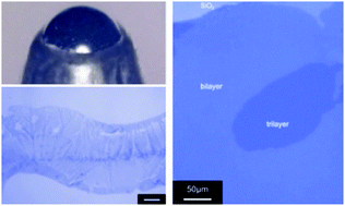
Directly writing 2D organic semiconducting crystals for high-performance field-effect transistors
2D organic semiconducting crystals written by a rollerball pen for high-performance transistors with a carrier mobility of up to 5.9 cm2 V−1 s−1.
J. Mater. Chem. C, 2017,5, 11246-11251
https://doi.org/10.1039/C7TC02348K
Optical properties and Raman-active phonon modes of two-dimensional honeycomb Zintl phases
We study how structure and stacking sequence influences the Raman spectra and band gaps in layered intermetallic Zintl phases comprised from honeycomb sheets of group 13, 14, and 15 elements.
J. Mater. Chem. C, 2017,5, 11259-11266
https://doi.org/10.1039/C7TC01907F
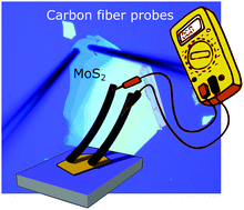
Lithography-free electrical transport measurements on 2D materials by direct microprobing
We present a method to test the electrical properties of 2D materials by directly contacting them with carbon fiber microprobes.
J. Mater. Chem. C, 2017,5, 11252-11258
https://doi.org/10.1039/C7TC01203A
About this collection
Also of interest