Ultralow power switching in a silicon-rich SiNy/SiNx double-layer resistive memory device
Abstract
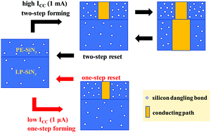
Here we demonstrate low-power resistive switching in a Ni/SiNy/SiNx/p++-Si device by proposing a double-layered structure (SiNy/SiNx), where the two SiN layers have different trap densities. The LRS was measured to be as low as 1 nA at a voltage of 1 V, because the SiNx layer maintains insulating properties for the LRS. The single-layered device suffers from uncontrollability of the conducting path, accompanied by the inherent randomness of switching parameters, weak immunity to breakdown during the reset process, and a high operating current. On the other hand, for a double-layered device, the effective conducting path in each layer, which can determine the operating current, can be well controlled by the ICC during the initial forming and set processes. A one-step forming and progressive reset process is observed for a low-power mode, which differs from the high-power switching mode that shows a two-step forming and reset process. Moreover, nonlinear behavior in the LRS, whose origin can be attributed to the P–F conduction and F–N tunneling driven by abundant traps in the silicon-rich SiNx layer, would be beneficial for next-generation nonvolatile memory applications by using a conventional passive SiNx layer as an active dielectric.


 Please wait while we load your content...