High-throughput electrical measurement and microfluidic sorting of semiconductor nanowires†
Abstract
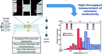
Existing nanowire electrical characterization tools not only are expensive and require sophisticated facilities, but are far too slow to enable statistical characterization of highly variable samples. They are also generally not compatible with further sorting and processing of nanowires. Here, we demonstrate a high-throughput, solution-based electro-orientation-spectroscopy (EOS) method, which is capable of automated electrical characterization of individual nanowires by direct optical visualization of their alignment behavior under spatially uniform electric fields of different frequencies. We demonstrate that EOS can quantitatively characterize the electrical conductivities of nanowires over a 6-order-of-magnitude range (10−5 to 10 S m−1, corresponding to typical carrier densities of 1010–1016 cm−3), with different fluids used to suspend the nanowires. By implementing EOS in a simple microfluidic device, continuous electrical characterization is achieved, and the sorting of nanowires is demonstrated as a proof-of-concept. With measurement speeds two orders of magnitude faster than direct-contact methods, the automated EOS instrument enables for the first time the statistical characterization of highly variable 1D nanomaterials.


 Please wait while we load your content...