Combinatorial insights into doping control and transport properties of zinc tin nitride†
Abstract
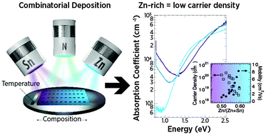
ZnSnN2 is an Earth-abundant semiconductor analogous to the III–nitrides with potential as a solar absorber due to its direct bandgap, steep absorption onset, and disorder-driven bandgap tunability. Despite these desirable properties, discrepancies in the fundamental bandgap and degenerate n-type carrier density have been prevalent issues in the limited amount of literature available on this material. Using a combinatorial RF co-sputtering approach, we have explored a growth-temperature-composition space for Zn1+xSn1−xN2 over the ranges 35–340 °C and 0.30–0.75 Zn/(Zn + Sn). In this way, we identified an optimal set of deposition parameters for obtaining as-deposited films with wurtzite crystal structure and carrier density as low as 1.8 × 1018 cm−3. Films grown at 230 °C with Zn/(Zn + Sn) = 0.60 were found to have the largest grain size overall (70 nm diameter on average) while also exhibiting low carrier density (3 × 1018 cm−3) and high mobility (8.3 cm2 V−1 s−1). Using this approach, we establish the direct bandgap of cation-disordered ZnSnN2 at 1.0 eV. Furthermore, we report tunable carrier density as a function of cation composition, in which lower carrier density is observed for higher Zn content. This relationship manifests as a Burstein–Moss shift widening the apparent bandgap as cation composition moves away from Zn-rich. Collectively, these findings provide important insight into the fundamental properties of the Zn–Sn–N material system and highlight the potential to utilize ZnSnN2 for photovoltaics.


 Please wait while we load your content...