Packaging commercial CMOS chips for lab on a chip integration†
Abstract
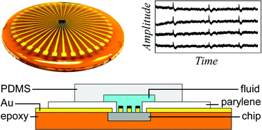
Combining integrated circuitry with microfluidics enables lab-on-a-chip (LOC) devices to perform sensing, freeing them from benchtop equipment. However, this integration is challenging with small chips, as is briefly reviewed with reference to key metrics for package comparison. In this paper we present a simple packaging method for including mm-sized, foundry-fabricated dies containing complementary metal oxide semiconductor (CMOS) circuits within LOCs. The chip is embedded in an epoxy handle wafer to yield a level, large-area surface, allowing subsequent photolithographic post-processing and microfluidic integration. Electrical connection off-chip is provided by thin film metal traces passivated with parylene-C. The parylene is patterned to selectively expose the active sensing area of the chip, allowing direct interaction with a fluidic environment. The method accommodates any die size and automatically levels the die and handle wafer surfaces. Functionality was demonstrated by packaging two different types of CMOS sensor ICs, a bioamplifier chip with an array of surface electrodes connected to internal amplifiers for recording extracellular electrical signals and a capacitance sensor chip for monitoring cell adhesion and viability. Cells were cultured on the surface of both types of chips, and data were acquired using a PC. Long term culture (weeks) showed the packaging materials to be biocompatible. Package lifetime was demonstrated by exposure to fluids over a longer duration (months), and the package was robust enough to allow repeated sterilization and re-use. The ease of fabrication and good performance of this packaging method should allow wide adoption, thereby spurring advances in miniaturized sensing systems.


 Please wait while we load your content...