Nonlinear current–voltage characteristics and enhanced negative differential conductance in graphene field effect transistors†
Abstract
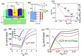
Recent observations of the negative differential conductance (NDC) phenomenon in graphene field-effect transistors (FET) open up new opportunities for their application in graphene-based fast switches, frequency multipliers and, most importantly, in high frequency oscillators up to the terahertz regime. Unlike conventional two-terminal NDC devices that rely on resonant tunneling and inter-valley transferring, in the present work, it has been shown that the universal NDC phenomenon of graphene-based FETs originates from their intrinsic nonlinear carrier transport under a strong electric field. The operation of graphene-NDC devices depends strongly on the interface between graphene and dielectric materials, the scattering-limited carrier mobility, and on the saturation velocity. To reveal such NDC behavior, the output characteristics of GFET are investigated rigorously, with both an analytical model and self-consistent transport equation, and with a multi-electrical parameter simulation. It is demonstrated that the contact-induced doping effect plays an important role in the operational efficiency of graphene-based NDC devices, rather than the ambipolar behavior associated with the competition between electron and hole conductances. In the absence of a NDC regime or beyond one, ambipolar transport starts at Vds > 2Vgs at the drain end, and as the dielectric layer begins to thin down, the kink-like saturation output characteristic is enhanced by the quantum capacitance contribution. These observations reveal the intrinsic mechanism of the NDC effect and open up new opportunities for the performance improvement of GFETs in future high-frequency applications, beyond the current paradigm based on two-terminal diodes.


 Please wait while we load your content...