
Graphene-based electrodes for enhanced organic thin film transistors based on pentacene†
Abstract
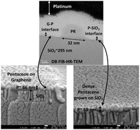
This paper presents 6,13-bis(triisopropylsilylethynyl)pentacene (TIPS-pentacene) and pentacene-based organic thin film transistors (OTFTs) with monolayer graphene source–drain (S–D) electrodes. The electrodes are patterned using conventional photolithographic techniques combined with reactive ion etching. The monolayer graphene film grown by chemical vapor deposition on Cu foil was transferred on a Si dioxide surface using a polymer-supported transfer method to fabricate bottom-gate, bottom-contact OTFTs. The pentacene OTFTs with graphene S–D contacts exhibited superior performance with a mobility of 0.1 cm2 V−1 s−1 and an on–off ratio of 105 compared with OTFTs with Au-based S–D contacts, which had a mobility of 0.01 cm2 V−1 s−1 and an on–off ratio of 103. The crystallinity, grain size, and microscopic defects (or the number of layers of graphene films) of the TIPS-pentacene/pentacene films were analyzed by X-ray diffraction spectroscopy, atomic force microscopy, and Raman spectroscopy, respectively. The feasibility of using graphene as an S–D electrode in OTFTs provides an alternative material with high carrier injection efficiency, chemical stability, and excellent interface properties with organic semiconductors, thus exhibiting improved device performance of C-based electronic OTFTs at a reduced cost.
 Please wait while we load your content...

