Inkjet printing and low temperature sintering of CuO and CdS as functional electronic layers and Schottky diodes
Abstract
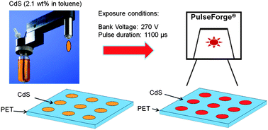
Here we report on inkjet printing of a conductive amorphous copper oxide (CuO) ink and of semiconducting

* Corresponding authors
a Fraunhofer Institute for Electronic Nano Systems (ENAS), Technologie-Campus 3, Chemnitz, Germany
b Chemnitz University of Technology, Institute for Print and Media Technology, Reichenhainer Straße 70, Chemnitz, Germany
c Laboratory of Organic and Macromolecular Chemistry (IOMC) and Jena Center for Soft Matter (JCSM), Friedrich-Schiller-University Jena, Humboldtstraße 10, Jena, Germany
d NovaCentrix, 200-B Parker Drive, Austin, Texas, USA
e
Selçuk University, Faculty of Engineering and Architecture, Department of Chemical Engineering, SU Advanced Technology Research and Application Center, Konya, Turkey
E-mail:
Nenad.Marjanovic@enas.fraunhofer.de
Here we report on inkjet printing of a conductive amorphous copper oxide (CuO) ink and of semiconducting

 Please wait while we load your content...
Something went wrong. Try again?
N. Marjanovic, J. Hammerschmidt, J. Perelaer, S. Farnsworth, I. Rawson, M. Kus, E. Yenel, S. Tilki, U. S. Schubert and R. R. Baumann, J. Mater. Chem., 2011, 21, 13634 DOI: 10.1039/C1JM11237F
To request permission to reproduce material from this article, please go to the Copyright Clearance Center request page.
If you are an author contributing to an RSC publication, you do not need to request permission provided correct acknowledgement is given.
If you are the author of this article, you do not need to request permission to reproduce figures and diagrams provided correct acknowledgement is given. If you want to reproduce the whole article in a third-party publication (excluding your thesis/dissertation for which permission is not required) please go to the Copyright Clearance Center request page.
Read more about how to correctly acknowledge RSC content.
 Fetching data from CrossRef.
This may take some time to load.
Loading related content
