Issue 13, 2018

High performance solution processed oxide thin-film transistors with inkjet printed Ag source–drain electrodes

Abstract

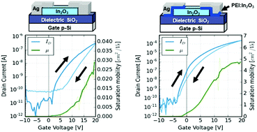
This letter reports the fabrication of inkjet-printed thin-film transistor devices employing an electron transport layer incorporating polyethyleneimine for engineering of the interface between In2O3 semiconductor and Ag source/drain contacts, resulting in significant enhancement of saturation mobility by two orders of magnitude, from ∼0.03 cm2 (V s)−1 to ∼3.0 cm2 (V s)−1. The improvement is assigned to the lowered contact resistance between the source/drain electrodes and the underlying layers. The results are of importance for fully-printed oxide TFTs and circuits.

Graphical abstract: High performance solution processed oxide thin-film transistors with inkjet printed Ag source–drain electrodes

Supplementary files

Article information

Article type
Communication
Submitted
11 Dec 2017
Accepted
12 Mar 2018
First published
13 Mar 2018

J. Mater. Chem. C, 2018,6, 3220-3225

High performance solution processed oxide thin-film transistors with inkjet printed Ag source–drain electrodes

L. Gillan, J. Leppäniemi, K. Eiroma, H. Majumdar and A. Alastalo, J. Mater. Chem. C, 2018, 6, 3220 DOI: 10.1039/C7TC05679F

To request permission to reproduce material from this article, please go to the Copyright Clearance Center request page.

If you are an author contributing to an RSC publication, you do not need to request permission provided correct acknowledgement is given.

If you are the author of this article, you do not need to request permission to reproduce figures and diagrams provided correct acknowledgement is given. If you want to reproduce the whole article in a third-party publication (excluding your thesis/dissertation for which permission is not required) please go to the Copyright Clearance Center request page.

Read more about how to correctly acknowledge RSC content.

Social activity

Spotlight

Advertisements