
A comprehensive study on carrier mobility and artificial photosynthetic properties in group VI B transition metal dichalcogenide monolayers†

Abstract
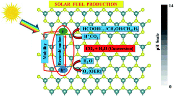
2D semiconducting transition-metal-dichalcogenides (TMDCs) have drawn a surge of research interests in ultra-thin nanoelectronics and optoelectronics, owing to their moderate charge carrier mobility. Due to a large variation in reported data on charge carrier mobilities of these free-standing monolayers, a more accurate determination of carrier mobilities is a must. This article highlights room temperature carrier mobilities calculated in group-VI B TMDC (i.e., MX2 (M = Mo, W; X = S, Se, Te)) monolayers via a systematic comparison of reliable models used within the framework of density functional theory. Additionally, piezoelectric effects on carrier mobility have been incorporated. The robust formulation by Lang et al. [Phys. Rev. B, 2016, 94, 235306] gives the most accurate estimation, where the carrier (i.e. electron or hole) mobility and the ratio of hole to electron mobility reach closest to the experimentally measured value. The higher mobility of holes with respect to electrons is attributed to the smaller deformation potential of the holes, while smaller carrier effective masses and larger elastic moduli cause larger carrier mobility in WX2 relative to MoX2. Carrier mobility is found to drop from S to Te and also from W to Mo in MX2 on account of the decrease in the elastic moduli, which is consistent with the increase in the macroscopic static dielectric constant. Erroneously high electron mobility (>1000 cm2 V−1 s−1), which is two orders of magnitude higher than the experimental ones, has been disputably reported earlier for MoTe2 and WS2 monolayers. It owes its origin to the ultrasmall deformation potential found therein. High (∼1.4–2.3) hole to electron mobility ratio in MX2 monolayers is found to occur in our work as MoSe2 > WS2 > MoS2 > WSe2 > WTe2 > MoTe2. This large carrier mobility ratio will facilitate an efficient separation of electron–hole pairs, which is particularly useful in optoelectronic applications, e.g., photovoltaics, photocatalysis and artificial photosynthesis. In all terms including optical absorbance, a WS2 monolayer is found to be most suitable for photophysical processes. Using the Nernst formulation, water splitting and CO2 photoreduction on WS2 are found to be favorable over a wide range of pH.
 Please wait while we load your content...

