
Quantifying atom-scale dopant movement and electrical activation in Si:P monolayers
 ab
Joseph A.
Hagmann,
a
ab
Joseph A.
Hagmann,
a
Abstract
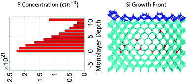
Advanced hydrogen lithography techniques and low-temperature epitaxial overgrowth enable the patterning of highly phosphorus-doped silicon (Si:P) monolayers (ML) with atomic precision. This approach to device fabrication has made Si:P monolayer systems a testbed for multiqubit quantum computing architectures and atomically precise 2-D superlattice designs whose behaviors are directly tied to the deterministic placement of single dopants. However, dopant segregation, diffusion, surface roughening, and defect formation during the encapsulation overgrowth introduce large uncertainties to the exact dopant placement and activation ratio. In this study, we develop a unique method by combining dopant segregation/diffusion models with sputter profiling simulation to monitor and control, at the atomic scale, dopant movement using room-temperature grown locking layers (LLs). We explore the impact of LL growth rate, thickness, rapid thermal annealing, surface accumulation, and growth front roughness on dopant confinement, local crystalline quality, and electrical activation within Si:P 2-D systems. We demonstrate that dopant movement can be more efficiently suppressed by increasing the LL growth rate than by increasing the LL thickness. We find that the dopant segregation length can be suppressed below a single Si lattice constant by increasing the LL growth rates at room temperature while maintaining epitaxy. Although dopant diffusivity within the LL is found to remain high (on the order of 10−17 cm2 s−1) even below the hydrogen desorption temperature, we demonstrate that exceptionally sharp dopant confinement with high electrical quality within Si:P monolayers can be achieved by combining a high LL growth rate with low-temperature LL rapid thermal annealing. The method developed in this study provides a key tool for 2-D fabrication techniques that require precise dopant placement to suppress, quantify, and predict a single dopant's movement at the atomic scale.
 Please wait while we load your content...

