Formation of in situ HVPE a-plane GaN nanodots: effects on the structural properties of a-plane GaN templates†
 *a
*a
Abstract
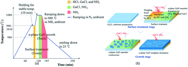
In situ a-plane GaN nanodots were formed on r-plane sapphire substrates to obtain a-plane GaN layers by using hydride vapor phase epitaxy (HVPE). The size and density of the GaN nanodots influence the juncture of the 2D growth of a-plane GaN, thus determining the density of threading dislocations and stacking faults as well as the surface morphology in growing a-plane GaN layers. Faster agglomeration in a-plane GaN layers via GaN nanodots with small size and high density leads to a decrease in the density of threading dislocations. A higher number of grain boundaries formed by nanodots with small size and high density are also responsible for a reduction in the number of stacking faults. Furthermore, we infer that the reduced atomic migration length difference of Ga and N along the c-axis and m-axis directions in GaN nanodots formed at low growth temperatures improved the surface morphology of a-plane GaN layers via the formation of a-plane GaN islands with an isotropic shape. We believe that this approach will provide a simple and efficient way to control the structural defects and surface undulations of a-plane GaN layers without any complex processes or additional expense.
 Please wait while we load your content...

