A high-performance fully nanostructured individual CdSe nanotube photodetector with enhanced responsivity and photoconductive gain†
 a
a
Abstract
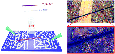
Defect-free and high-quality CdSe nanotubes (NTs) have been prepared via a simplified one-step ambient pressure physical vapor deposition (APPVD) process using CdSe powder as the precursor compound. Based on the CdSe nanotubes grown using this method, a metal–semiconductor–metal (MSM) nanostructured photodetector with an individual CdSe nanotube as the active layer and Ag nanowire (NW) networks of low resistivity and high transmissivity as electrodes was fabricated and characterized. Owing to the perfect hollow tubular architecture of the CdSe nanotube and the Schottky contacts between Ag and CdSe, the individual CdSe NT-based photodetector exhibits excellent performance, demonstrating the largest responsivity (1.17 × 10⁷ A W−1), photoconductor gain (2.93 × 10⁷), specific detectivity (4.53 × 1015 cm Hz1/2 W−1) and high sensitivity (2023) among the CdSe nanostructures based photodetectors reported to date. When the devices work in vacuum, a further enhancement in the photodetector performances is demonstrated. Moreover, a physical model based on band energy theory provides access to understanding the carrier transport in such nanostructured MSM devices.
 Please wait while we load your content...

