
Recent developments in III–V semiconducting nanowires for high-performance photodetectors
 *bcd
*bcd
Abstract
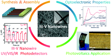
Recently, high-performance III–V semiconductor nanowires (NWs) have been extensively explored as promising active material candidates for high-sensitivity and broad-spectrum photodetectors operating at room temperature, which would have potential application in integrated optoelectronic devices for photovoltaics, radiation imaging, sensing, and information communications and processing. In this review, we present a comprehensive overview of the recent advances in the study of III–V NW-based photodetectors operating in the UV, visible and infrared spectral range, starting from the cost-effective synthesis and assembly of III–V NWs, the precise manipulation of their optoelectronic properties, and all the way to their different types of utilizations in photodetection and solar cells. Specifically, the synthesis methods and growth mechanisms of typical III–V NWs are discussed, emphasizing the low-cost solid-source chemical vapor deposition (CVD) technique, which has been widely employed in the growth of various III–V NW materials due to the setup simplicity as well as the excellent process controllability. The optoelectronic properties of these synthesized NWs, such as light absorption and photoconductive gain, are then investigated accordingly. Effective light absorption and extremely high photoconductive gain have been demonstrated, confirming their suitability as active components for photodetector applications. By utilizing the recently developed contact printing method, high-performance III–V NW solar cells can also be easily integrated on the glass and plastic substrates for transparent and flexible photovoltaics, which explicitly indicates the outstanding versatility and promising perspective of these NW Schottky photovoltaics for next-generation smart solar energy harvesting devices. Towards the end, we also discuss the progress made and the challenges in the research of high-performance photodetectors and photovoltaic devices based on III–V NWs.
- This article is part of the themed collection: 2017 Materials Chemistry Frontiers Review-type Articles
 Please wait while we load your content...

