
Seed-mediated phase-selective growth of Cu2GeS3 hollow nanoparticles with huge cavities†

Abstract
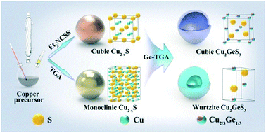
Although significant progress has been achieved in the synthesis of hollow nanoparticles (NPs), research on copper-based multinary chalcogenide (CMC) semiconductor NPs with hollow structures is still less developed. In this work, we demonstrate an effective method for the phase-selective synthesis of cubic Cu2GeS3 hollow NPs (HNPs) with huge cavities and thin shells. This method includes the nucleation of Cu2−xS seeds, followed by unequal diffusion between Cu+ and Ge4+. A common rule for the phase-selective growth of CMC NPs has been revealed: the nucleation step is the crystal phase-determining step in the growth process of CMC NPs, and the sulfur sources govern the crystal phase of the nucleus. Because of their huge cavities, the as-prepared large Cu2GeS3 HNPs are proved to be macroporous materials with a specific surface area of 22.1 m2 g−1. Besides, cubic Cu2GeS3 HNPs with small cavities are also synthesized, following the same method with little modification. By integrating the advantages of the large Cu2GeS3 HNPs (high surface-to-volume area) and the small Cu2GeS3 HNPs (good dispersibility and monodispersity), a new kind of two-layer photoelectrode is prepared. Compared with the photoelectrodes prepared using pure large and small Cu2GeS3 HNPs, the two-layer photoelectrode exhibits superior performance for photoelectrochemistry due to the high interface area of the upper layer and the ideal compactness of the bottom layer.
 Please wait while we load your content...

