
Metal-substrate-supported tungsten-oxide nanoarrays via porous-alumina-assisted anodization: from nanocolumns to nanocapsules and nanotubes†
Abstract
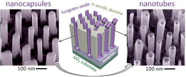
An array of highly aligned tungsten-oxide (TO) nanorods, ∼80 nm wide, up to 900 nm long, spatially separated at their bottoms by tungsten metal on a substrate is synthesized via the self-localized anodization of aluminum followed by the porous-alumina-assisted re-anodization of tungsten in a sputter-deposited Al/W bilayer. Moreover, the pore-directed TO nanocapsules may grow, which can be electrochemically top-opened in alumina nanopores and transformed to TO nanotubes, representing unique architectures built up on tungsten substrates to date. The as-grown nanorods are composed of amorphous WO3 mixed with minor amounts of WO2 and Al2O3 in the outer layer and oxide–hydroxide compound (WO3·nH2O) with aluminum tungstate (2Al2O3·5WO3), mainly present inside the rods. Once the growing oxide fills up the pores, it comes out as an array of exotic protuberances of highly hydrated TO, with no analogues among the other valve-metal oxides. Vacuum or air annealing at 550 °C increases the portion of non-stoichiometric oxides ‘doped’ with OH-groups and gives monoclinic WO2.9 or a mixture of WO3 and WO2.9 nanocrystalline phases, respectively. The nanorods show n-type semiconductor behavior when examined by Mott–Schottky analysis, with a high carrier density of 7 × 10¹⁹ or 3 × 1019 cm−3 for the air- or vacuum-annealed samples, associated with a charge depletion layer of about 8 or 10 nm, respectively. A model for the growth of the metal-substrate-separated TO nanocapsules and tubes is proposed and experimentally justified. The findings suggest that the new TO nanoarrays with well-defined nano-channels for carriers may form the basic elements for photoanodes or emerging 3-D micro- and nano-sensors.
 Please wait while we load your content...

