Energy band diagram of device-grade silicon nanocrystals†
Abstract
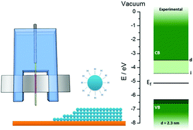
Device grade silicon nanocrystals (NCs) are synthesized using an atmospheric-pressure plasma technique. The Si NCs have a small and well defined size of about 2.3 nm. The synthesis system allows for the direct creation of thin films, enabling a range of measurements to be performed and easy implementation of this material in different devices. The chemical stability of the Si NCs is evaluated, showing relatively long-term durability thanks to hydrogen surface terminations. Optical and electrical characterization techniques, including Kelvin probe, ultraviolet photoemission spectroscopy and Mott–Schottky analysis, are employed to determine the energy band diagram of the Si NCs.
 Please wait while we load your content...

