This website uses cookies to give you the best user experience. If you continue
without changing your settings we'll assume you are happy to receive all RSC cookies.
You can change your cookie settings by navigating to our Privacy and Cookies page and following the instructions. These instructions
are also obtainable from the privacy link at the bottom of any RSC page.
Department of Mechanical Engineering, University of Connecticut, 191 Auditorium Road, Unit 3139, Storrs, USA
E-mail: wchiu@engr.uconn.edu
; Tel: +860-486-3647
b
Center for Innovative Fuel Cell and Battery Technologies, School of Materials Science and Engineering, Georgia Institute of Technology, Atlanta, USA
E-mail: meilin.liu@mse.gatech.edu
; Tel: +404-894-6114
c
Advanced Photon Source, Argonne National Laboratory, Building 401, 9700 South Cass Avenue, Argonne, USA
E-mail: yuwang@aps.anl.gov
; Tel: +630-252-3789
d
NSLS-II, Brookhaven National Laboratory, Upton, USA
E-mail: ychu@bnl.gov
; Tel: +631-344-5582
Nanoscale, 2012,4, 1557-1560
DOI:
10.1039/C2NR11690A
Received
09 Nov 2011,
Accepted
06 Jan 2012
First published online
10 Jan 2012
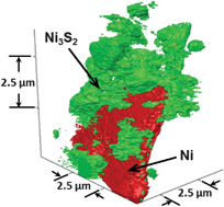
Nano-structures of nickel (Ni) and nickel subsulfide (Ni3S2) materials were studied and mapped in 3D with high-resolution x-ray nanotomography combined with full field XANES spectroscopy. This method for characterizing these phases in complex microstructures is an important new analytical imaging technique, applicable to a wide range of nanoscale and mesoscale electrochemical systems.
Fetching data from CrossRef. This may take some time to load.