
 Open Access Article
 This Open Access Article is licensed under a Creative Commons Attribution-Non Commercial 3.0 Unported Licence
A triboelectric nanogenerator with synergistic complementary nanopatterns fabricated by block copolymer self-assembly†
Seong-Yun
Yun‡
a,
Min Hyeok
Kim‡
b,
Geon Gug
Yang
b,
Hee Jae
Choi
b,
Do-Wan
Kim
a,
Yang-Kyu
Choi
 *ac and
Sang Ouk
Kim
*bc
*ac and
Sang Ouk
Kim
*bc
aSchool of Electrical Engineering, Korea Advanced Institute of Science and Technology (KAIST), 291 Daehak-ro, Daejeon 34141, Republic of Korea
bNational Creative Research Initiative Center for Multi-dimensional Directed Nanoscale Assembly, Department of Materials Science and Engineering, KAIST, 291 Daehak-ro, Yuseong-gu, Daejeon 34141, Republic of Korea
cKAIST Institute for Nanocentury, KAIST, 291 Daehak-ro, Yuseong-gu, Daejeon 34141, Republic of Korea
First published on 25th March 2024
Abstract
Triboelectric nanogenerators (TENGs) are promising candidates for self-powered sensors or power supplies, with advantages of low production cost and facile fabrication. The electrical output performance of TENGs can be enhanced by increasing the effective contact area between triboelectric materials. However, typical methodologies to improve surface roughness, including photolithography, commonly suffer from high processing cost and limited selection of materials. Herein, a TENG with complementary nanopatterns (CN-TENG), synergistically composed of protruded metals (gold) and indented polymers (Teflon), is fabricated by means of block copolymer (BCP) self-assembly, while adjusting the molecular weight (MW) of the BCPs. Mussel-inspired polydopamine treatment was applied to optimize the interfacial energy of the chemically inert triboelectric material surfaces for desirable BCP nanopatterning. The resultant nanopatterned pairs were systematically classified into nine types of combinations to exploit the interplay among different patterned morphologies. The CN-TENG yielded substantially improved electrical outputs compared to the nonpatterned counterpart and a spatially designed array consisting of six CN-TENGs was successfully utilized for a gait monitoring system to detect gait abnormalities.
Introduction
Along with rapid advances in sustainable and energy-efficient wearable devices, energy harvesting is becoming increasingly demanded to convert various types of wasted energy, such as natural sunlight, wind, sea water current and residual heat, into valuable resources of electricity.1–4 As one of the most pervasive energy sources, ubiquitous mechanical energy generated from humans and nature can be effectively converted into electrical energy by utilizing several different mechanisms. In particular, triboelectric nanogenerators (TENGs) that exploit the mechanisms of contact electrification and electrostatic induction have attracted considerable research attention owing to the unique benefits arising from a wide range of material selection, relatively low production cost, a simple fabrication route, and other factors.5,6 To effectively enhance the electrical output of TENGs, a high charge density should be induced on each triboelectric layer under repetitive nonperiodic contact-separation cycles.7Typical strategies to enhance the surface charge density of triboelectric layers include chemical modification, environmental control, and physical modification. Chemical modification entails altering the surface or bulk properties of triboelectric materials with surface functionalization or controlling the charge-trapping capability by surface polarization.8,9 Environmental changes encompass adjusting various ambient parameters, such as temperature and ambient composition.10,11 Physical modification commonly involves roughening the triboelectric layers to enhance the effective contact area. This can be achieved by a large-area scalable nanofabrication process, such as electrochemical anodization of metal surfaces or straightforward nanopatterning of polymeric materials.12,13 It is noteworthy that solid–liquid contact electrification can also be introduced to increase the effective contact area significantly, thanks to the excellent shape adaptability of liquids.14 In a similar way, when a nanoscale patterning strategy is applied to a soft material, which is selected as the triboelectric layer for enhanced structural stability of a TENG, the effective contact area can also be enhanced, particularly taking advantage of elastic deformability.15–19
For effective nanopatterning of arbitrary functional surfaces, two major types of patterning strategies are available, top-down photolithography and bottom-up self-assembly. Top-down photolithography has long been widely used in the broad industrial areas of semiconductor and display devices but shows critical weaknesses for TENG application, including relatively high processing cost with expensive facilities, intrinsic resolution limits governed by optics, and limited manufacturability on nonplanar and flexible substrates, which are widely used for TENGs. By contrast, a bottom-up approach relying on block copolymer (BCP) self-assembly is a strong candidate to overcome those challenges. BCP is a type of macromolecular material consisting of two or more chemically different polymer blocks mutually connected by covalent bonding. These chemically distinctive polymer blocks undergo spontaneous microphase separation, whose characteristic length scales are defined by the molecular dimension.20,21 Accordingly, nanosized periodic patterns are delineated by the inherent scalable self-assembly of BCPs to build up large-area patterned structures, consisting of nanoscale spheres, cylinders, lamellae, and so on.22–26 The characteristic pattern size ranging from 5 to 100 nm as well as the pattern shape can be precisely defined by controlling the molecular weight (MW) and compositional fractions in BCPs.27 Notably, such nanoscale patterns are readily transferrable to arbitrary functional material surfaces by means of soft lithography strategies without requiring high-cost equipment. Even though there have been research efforts for BCP-based TENGs, it is still required to investigate into shape and size effects of nanoscale patterns.28,29
In this work, a high performance TENG with synergistic complementary nanopatterns at both sides of the triboelectric layers (hereafter abbreviated as CN-TENG) was developed by employing BCP-based self-assembled nanoscale patterning. We employed polystyrene-block-polymethylmethacrylate (PS-b-PMMA) BCPs with various MW and compositional fractions. The PS self-assembled nanodomains, remaining after selective removal of PMMA nanodomains, acted as mask layers for subsequent pattern transfer by area-selective etching or deposition. Notably, PS-b-PMMA cannot define surface perpendicular oriented lamellar or cylindrical nanopatterns directly on inert gold (Au) or Teflon surfaces. Therefore, mussel-inspired surface engineering using a polydopamine (PDA) treatment was employed to obtain neutral interfacial energy towards the PS and PMMA components.30
In the subsequent nanofabrication process replicating BCP self-assembled morphologies, protruded nanopatterns were formed on Au surfaces by electron-beam evaporated deposition and subsequent lift-off, whereas indented nanopatterns were engraved on Teflon surfaces by CF4 plasma etching. When the protruded and indented nanopatterns originated from the same parent BCPs, they were likely to complement each other, similar to a lock-and-key combination. Based on the pattern shape and size at each side, nine different pairs were identified from the combinations of Au patterns (flat, nanowires, and nanodots) and Teflon patterns (flat, nanotrenches, and nanopores). The CN-TENG with complementary pairs of an Au nanodot pattern and a Teflon nanoporous pattern showed the highest electrical outputs and was utilized for a gait monitoring system by implementing a designed array of six CN-TENGs at the bottom of shoes. While harvesting electrical energy from three different types of mechanical locomotion, walking, running, and jumping, the gait monitoring system could successfully detect two typical abnormalities in the gait patterns (in-toeing and out-toeing).
Experimental section
Fabrication of nanopatterns
The upper part of the TENG consists of three layers, a thick acryl plate with 1 cm thickness at the top, a polyimide sheet with 150 μm thickness in the middle, and an Au layer with 40 nm thickness at the bottom (Fig. 1a). The Au layer was deposited by electron-beam evaporated physical vapor deposition (SNTEK) onto the polyimide sheet. The lower part of the TENG consists of four layers, a Teflon (CHUKOH) layer with 80 μm thickness at the top, an Au layer with 40 nm thickness in the upper middle, a polyimide sheet with 150 μm thickness in the lower middle, and another thick acryl plate with 1 cm thickness at the bottom. The effective footprint size of each layer is 3 cm × 3 cm. For the mussel-inspired surface engineering of inert surfaces, a sample of Au deposited on the polyimide and a counter sample of Teflon on the polyimide were immersed in 2 g L−1 dopamine hydrochloride solution, mixed with 10 mM Tris buffer solution (Sigma-Aldrich) for about one hour. At a pH of 8.5, dopamine hydrochloride was polymerized into polydopamine, and deposited at the Au and Teflon surfaces. After the surfaces were recovered from the solution, rinsed, and dried, 1 wt% PS-r-PMMA solution in toluene was spin-coated onto the dopamine-treated Au and Teflon surfaces. Afterwards, they were thermally annealed at 160 °C in a vacuum oven overnight to graft the random copolymer brushes. After the neutral brush treatment, 2 wt% PS-b-PMMA BCP solution (polymer sources) in toluene was then spin-coated on the brush-treated surface. Here, by using solutions with different molecular weights of the BCP, nanopatterns with lamellar and cylindrical morphologies could be obtained. Solvent annealing of the BCP-deposited substrates for three hours under tetrahydrofuran vapor successfully induced self-assembled nanopatterns. The PMMA nanodomains in the self-assembled BCP film were selectively etched by reactive ion etch (RIE) with O2 gas, leaving the topographic PS nanodomains, which were subsequently used as a mask layer for further pattern transfer with selective etching or deposition. | ||
| Fig. 1 (a) Schematic illustration of the triboelectric nanogenerator with synergistic complementary nanopatterns at both sides of triboelectric layers (CN-TENG) and surface modification process on Teflon and gold. (b) Scanning electron microscope (SEM) image of the cylinder phase PS-b-PMMA template. (c) SEM image of indented Teflon nanopores transferred from the cylinder phase PS-b-PMMAtemplate. (d) SEM image of protruded gold nanodots. (e) SEM image of the lamellar phase PS-b-PMMA template. (f) SEM image of indented Teflon nanotrenches transferred from the lamellar phase PS-b-PMMA template. (g) SEM image of protruded gold nanowires. | ||
Characterization
Morphologies of the nanopatterns formed on the Teflon and Au surfaces were characterized using a scanning electron microscope (S-4800, Hitachi). Fast Fourier transform (FFT) and binarization of SEM images were conducted using ImageJ software. To check the periodicity of the nanopatterns, grazing-incidence small-angle X-ray scattering (GISAXS) analysis was conducted with the 9A beamline in the Pohang Accelerator Laboratory (PAL). Water contact angle analysis (Phoenix, SEO) and X-ray photoelectron spectroscopy (XPS (K-alpha, Thermo Scientific)) were also conducted to analyze the surface properties and chemical composition of the Teflon nanopatterns. To measure the electrical output from CN-TENGs, an electrometer (6514, Keithley) was utilized. A function generator (33![[thin space (1/6-em)]](https://www.rsc.org/images/entities/char_2009.gif) 120, hp) was used to induce the electrical signal with a frequency of 3 Hz. To convert the electrical signal into mechanical motion, an electrodynamic shaker (LW-140-110, Lab-works) was used. A force sensor (208C02, PCB Piezoelectronics) was employed to characterize the contact force. A data acquisition (DAQ) board was utilized to acquire electrical signals from the CN-TENG array for the gait monitoring system. The photographs of the CN-TENGs and corresponding experimental benches are shown in Fig. S1.†
120, hp) was used to induce the electrical signal with a frequency of 3 Hz. To convert the electrical signal into mechanical motion, an electrodynamic shaker (LW-140-110, Lab-works) was used. A force sensor (208C02, PCB Piezoelectronics) was employed to characterize the contact force. A data acquisition (DAQ) board was utilized to acquire electrical signals from the CN-TENG array for the gait monitoring system. The photographs of the CN-TENGs and corresponding experimental benches are shown in Fig. S1.†
Results and discussion
Fabrication and characterization of nanopatterns
Schematic illustrations of the proposed CN-TENG device structures, utilizing the triboelectrification between Au and Teflon, are shown in Fig. 1a, along with brief descriptions of the fabrication procedures. A polyimide sheet with 150 μm thickness was selected as a substrate, considering its high thermal and chemical stability. Au served as an electrode as well as a triboelectric layer prone to be positively charged. It has high electrical conductivity and is located at the upper positive end of the triboelectric series. Teflon acted as the counter triboelectric layer, motivated by its lower negative position in the triboelectric series, arising from its strong electron-accepting properties. Nanopatterns on the Au and Teflon layers were fabricated by replicating the self-assembled nanopatterns from PS-b-PMMA BCPs. BCPs with PS molecular weight of 132 kg mol−1 and PMMA molecular weight of 68 kg mol−1 self-assembled into a hexagonally arranged nanoscale cylinder morphology, as shown in Fig. 1b. Similarly, a lamellar phase self-assembled morphology was created from the BCPs with PS of 105 kg mol−1 and PMMA of 106 kg mol−1, as shown in Fig. 1e.The PMMA nanodomains in the self-assembled morphology of PS-b-PMMA BCPs were selectively removed by O2 RIE. The remaining topographic structure consisting of PS nanodomains served as a masking layer (PS mask) for further pattern transfer. The Teflon layer underneath the PS mask was etched by RIE with inductively coupled CF4 plasma. Accordingly, the nanopatterns in the PS mask were precisely replicated onto the underlying Teflon layer. The PS mask with a cylinder phase left an indented hexagonal nanoporous pattern, while that with a lamellar phase created indented nanotrenches, as shown in Fig. 1c and f, respectively. By contrast, protruded Au nanopatterns could be formed by Au deposition with an electron-beam evaporation process and subsequent lift-off of the pattern masks. The PS mask with a cylinder phase left a protruded Au nanodot pattern, while that with a lamellar phase created Au nanowires, as respectively shown in Fig. 1d and g. Details of the fabrication process are provided in the Experimental section (Fig. S2†). It is noteworthy that such nanopatterns could be fabricated on a 6-inch wafer, indicating the potential for a large-scale fabrication process by BCP self-assembly (Fig. S3†).
It is important to modify the surface energy of a target surface by using a PS-r-PMMA random copolymer brush layer to induce vertically aligned lamellar or cylinder nanopatterns of PS-b-PMMA BCPs. Unfortunately, direct surface modification of Teflon is difficult due to its extremely low surface energy. To address this inherent issue, mussel-inspired surface engineering was employed. Fig. 2a provides a schematic illustration of the BCP self-assembly process on Teflon surfaces with and without PDA treatment. Without the PDA layer, the PS-r-PMMA brush layer could not be stabilized on the inert Teflon surface. By contrast, upon PDA treatment, vertically oriented lamellar or cylinder nanopatterns of PS-b-PMMA BCPs could be successfully induced, depending on the volume fraction between PS and PMMA components. Fig. 2b displays a plane view SEM image for the vertically aligned PS-b-PMMA BCP nanopatterns formed on a Teflon surface. Fig. 2c and d contrast the water contact angles on the Teflon surfaces before and after PDA treatment. The initially hydrophobic surface of bare Teflon could be successfully rendered hydrophilic by PDA treatment. Consequently, vertically aligned PS-b-PMMA nanopatterns could be well-stabilized on the Teflon surfaces.
 | ||
| Fig. 2 (a) Schematic illustration of polydopamine (PDA) treatment during Teflon patterning via a block copolymer (BCP). (b) Top view SEM image of vertically-aligned PS-b-PMMA BCP nanopatterns on Teflon with PDA treatment. (c) Water contact angle on Teflon without PDA treatment. (d) Water contact angle on Teflon with PDA treatment. (e) Fast Fourier transform (FFT) data extracted from the SEM image of cylinder phase PS-b-PMMA. (f) FFT data extracted from the SEM image of lamellar phase PS-b-PMMA. (g) Grazing-incidence small-angle X-ray scattering (GISAXS) data of Teflon nanopores, (h) GISAXS data of gold nanodots. (i) GISAXS data of Teflon nanotrenches. (j) GISAXS data of gold nanowires. | ||
The precise nanopattern size in the BCP layer was analyzed with an FFT analysis of SEM images. Fig. 2e and f present the FFT data for the cylinder phase pattern with 58.3 nm pattern periodicity (Fig. 1b) and the lamellar phase pattern with 70.2 nm periodicity (Fig. 1e), respectively. Similarly, Fig. S4† shows the FFT data for the indented Teflon patterns with nanoporous and nanotrench morphologies after PMMA etching and for the protruded Au patterns consisting of nanodot and nanowire morphologies after the lift-off process. The nanopatterns on Teflon and Au were also analyzed with GISAXS. Fig. 2g and h show GISAXS results for the Teflon nanoporous and Au nanodot patterns, respectively. The pattern periodicities calculated from the GISAXS peak positions were 62.8 and 60.8 nm, respectively. From the peak positions shown in Fig. S5a and S5b,† it was confirmed that the nanopatterns form hexagonally-packed cylindrical structures across the entire sample areas. Fig. 2i and j show the GISAXS data for the Teflon nanotrench and Au nanowire patterns, respectively, whose pattern periodicities were confirmed to be 74.2 and 69.5 nm, respectively. It could also be verified that the nanopatterns of Teflon nanotrenches and Au nanowires were well-formed across the entire sample areas (Fig. S5c and S5d†). It is noteworthy that it is also important to check whether the nanopatterns were successfully transferred onto the underlying Teflon layer without PS-r-PMMA or PDA residue. XPS was utilized to detect any residue on the patterned Teflon surfaces (Fig. S6†). As a reference, a bare Teflon sample was also characterized. While the nonpatterned reference showed C–F2 and C–C bonding, the nanopatterned sample exhibited additional peaks such as C–CFx, C–F, and C–F3 bonding, arising from the bond breakage under CF4 etching. Nonetheless, no residue from the PS-r-PMMA BCPs or PDA layer was detected. Noticeably, it was confirmed that such a modification of surface composition does not significantly influence the performance of TENGs (Fig. S7†).
Effect of complementary nanopatterns in the CN-TENG
Fig. 3a shows a schematic illustration of the proposed working principle of CN-TENG devices. The upper triboelectric layer is composed of a 10 nm thick Au electrode deposited upon a polyimide sheet (150 μm). The lower electrode layer corresponds to the 80 μm thick Teflon layer stabilized upon the Au electrode surface (40 nm). When the Au and Teflon layers contact each other, the Au surface becomes positively charged, whereas the Teflon surface is negatively charged, according to their relative positions in the triboelectric series.31,32 Upon the following separation, the positive charges at the upper Au electrode migrate toward the lower Au electrode, driven by electrostatic induction. The upper Au electrode becomes electrically neutral after the complete separation. When the two electrodes become close again, the positive charges on the lower Au electrode move toward the upper Au electrode. Accordingly, the CN-TENG generates alternating current under the repeated contact-separation cycles. Fig. 3b demonstrates effective lighting up of a light-emitting diode (LED) by hand-tapping a CN-TENG device.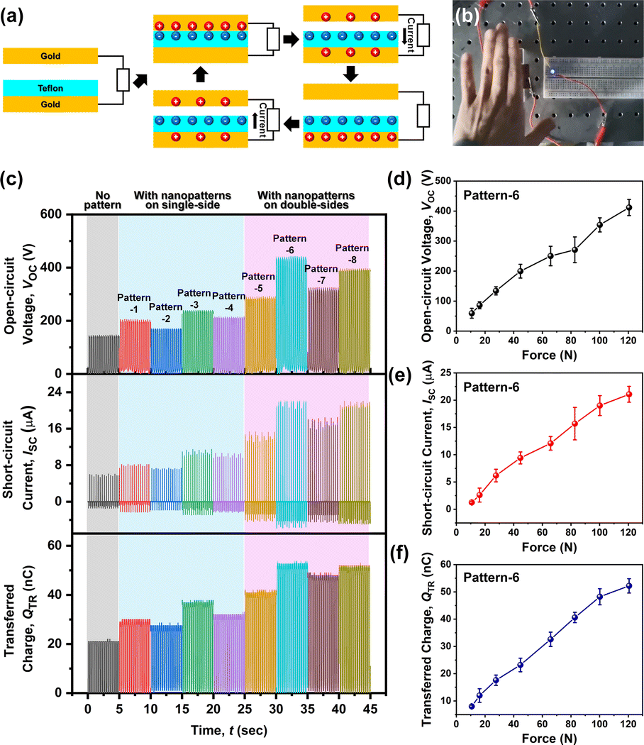 | ||
| Fig. 3 (a) Operation mechanism of the proposed CN-TENG in contact-separation mode. (b) Actual device operation with hand-tapping. (c) Electrical outputs from the 9 types of TENGs without and with nanopatterns. (d) Measured VOC (e) ISC, and (f) QTR from five CN-TENGs with gold nanodots and Teflon nanopores (pattern-6). | ||
To investigate the influence of different nanopattern combinations, various CN-TENGs were prepared with various BCP template structures. In the upper Au electrode, three different pattern shapes were prepared, flat Au without any pattern, Au with a nanowire pattern, and Au with a nanodot pattern. The bottom Teflon layer was also one of the three types, flat Teflon without any pattern, Teflon with a nanotrench pattern, and Teflon with a nanoporous pattern. Overall, nine combinations of TENGs were prepared, as summarized in Table S1.† For each combination, five TENGs were independently fabricated. Fig. 3c compares the open-circuit voltage (VOC), short-circuit current (ISC), and transferred charge (QTR) values measured from the TENG devices. For this measurement, the applied force and frequency were fixed to 120.6 N and 3 Hz, respectively. Detailed measurement settings in the electrometer are shown in Fig. S8.† The respective values for the TENG with flat Teflon and flat Au layers (no pattern) were 145.9 V, 5.9 μA, and 21.0 nC. The TENGs with the nanopatterns only at one side of the triboelectric layer (patterns-1, 2, 3, and 4) showed higher performance than that of the nonpatterned flat TENG. Notably, the VOC, ISC, and QTR values of the CN-TENGs incorporating the nanopatterns at both sides of the triboelectric layers (patterns-5, 6, 7, and 8) became even higher. This is attributed to the complementary nanopatterns offering the largest interfacial contact areas offered by while mimicking a ‘lock-and-key’ structure. It is noteworthy that this clear tendency is consistent with previous studies on high-performance TENGs with the triboelectric layers complementarily patterned at both sides.33,34 The highest VOC, ISC, and QTR values were obtained from the CN-TENG with an Au nanodot pattern and a Teflon nanoporous pattern (pattern-6): 442.0 V, 22.2 μA, and 53.9 nC, respectively. The electrical outputs from the CN-TENG with complementary pattern-6 are roughly three times larger than those from the TENG without any pattern. It is noteworthy that pattern-6 and pattern-8 showed higher performances compared to pattern-5 and pattern-7, as gold nanodots can effectively penetrate the indented Teflon nanostructure, including nanopores, and nanotrenches, whereas randomized gold nanowires replicating fingerprint like lamellar structures cannot penetrate those structures. This supports that the mutually interlocking structure of the two electrode surfaces is essential for high-performance TENGs. To investigate the effect of surface roughness, we determined a contact area factor from Fig. 1b to g, which indicates how much the contact area increases due to the surface roughness increased by patterning. Fig. S9† shows the relationship between the contact areas of the TENG devices and the corresponding normalized output values, demonstrating a typical proportional relationship. It is noteworthy that previous research efforts for BCP-based TENGs have just focused on enhancing the device performance without systematic study on the effects of the topographic nanoscale pattern shape.28,29Fig. 3d–f show the electrical outputs of VOC, ISC, and QTR according to the applied force for the CN-TENG with pattern-6, respectively. There is a linear relationship between the electrical outputs and the applied force, indicating that the CN-TENG can be used as a pressure-based self-powered sensor.
The effect of contact-separation frequency was also investigated for the CN-TENG with pattern-6. A function generator was used to control the frequency. As shown in Fig. S10,†ISC increased when the frequency increased from 0.5 Hz to 4.0 Hz. A higher frequency value of contact separation shortens the current flow time and increases the rate of charge transfer between two electrodes of the CN-TENG. On the other hand, because the rate of charge transfer is still larger than the speed of the applied force, QTR remained unchanged with different frequencies. VOC also remained unchanged because the charge transfer process is not involved under the open-circuit conditions. These results are consistent with the previous theoretical report.35
Fig. 4a displays the output voltage (Vout) and output current (Iout) values of the TENG devices with pattern-6 depending on the load resistance (Rload). Vout tends to increase with Rload as charge transfer is limited, whereas Iout decreases.35,36Fig. 4b exhibits the output power (Pout), calculated from the Iout measured at each Rload. The power generated by the CN-TENG could be visualized by lighting up a set of LEDs directly connected to the CN-TENG and a rectifying circuit (Fig. S11a†). While the TENG without any pattern lit up 200 LEDs by hand-tapping (Fig. S11b†), that with pattern-6 lit up more than 400 LEDs under the same experimental conditions (Fig. S11c†).
 | ||
| Fig. 4 (a) Dependency of output current (Iout) and voltage (Vout) of the CN-TENG with pattern-6 according to various load resistance (Rload) values. (b) Dependency of the output power (Pout) of the same CN-TENG according to various Rload values. (c) Measured VOC up to 60000 cycles of contact and separation from the CN-TENG with pattern-6. (d) Measured VOC from the CN-TENGs with pattern-6 and the TENG without any pattern for different relative humidity (RH). These electrical data per each condition were measured from five CN-TENGs. | ||
It is necessary to investigate the influence of the critical nanopattern size used for the proposed CN-TENG upon the corresponding device performance. Among the nine pairs with different nanopattern combinations, the CN-TENG with pattern-6 showing the highest electrical outputs was selected for three sub-splits (size-1, size-2, and size-3 in ascending order of the critical pattern size) in their pattern sizes (Fig. S12a–d†), which could be readily controlled by employing different MW of BCPs (Table S2†). The electrical output values measured from the CN-TENGs with the above three sub-splits (Fig. S12e–g†) do not show significant differences in the electrical output values. Thus, it could be deduced that the shape of the nanopattern is more important than the size of the nanopattern for effective control of the TENG performance.
It is also important to evaluate the reliability and stability of the proposed CN-TENG devices. A durability test under repeated operation was conducted up to 60000 cycles of contact-separation cycles. As shown in Fig. 4c, there was no noticeable degradation in VOC over the prolonged cycles of device operation. Fig. 4d presents the electrical output values measured at various levels of relative humidity (RH). The TENG devices without any pattern and pattern-6 commonly revealed gradual degradation of VOC, particularly when the RH level was above 55%. Nonetheless, the device with pattern-6 still generates a higher VOC, even compared to the VOC of the TENG without any pattern at a RH of 20%. This verifies that the performance improvement resulting from the enlarged contact area with the complementary nanopatterns may outweigh the performance degradation caused by high humidity under the ambient conditions.
Self-powered sensor to monitor abnormal gait
Gait abnormality commonly observed in childhood can be a significant cause of deformities.37,38 As a practical application of the proposed high performance TENG with complementary nanopatterns, a gait monitoring system could be demonstrated.39–44Fig. 5a presents comprehensive schematics of the gait monitoring system. Six CN-TENG devices (cells #1, #2, #3, #4, #5, and #6) with pattern-6 were affixed to the outsole of a shoe to detect mechanical pressure generated upon human locomotion. It is noteworthy that this set of CN-TENG patterns was incorporated into the outsole for convenience in implementing cables directly connected to a DAQ board. For the eventual practical application, however, it would be more desirable to install them beneath an insole for long-term use. The length and width of each CN-TENG device were 2 cm by 2 cm. Vout signals generated by the CN-TENG array were measured by using a DAQ board. | ||
| Fig. 5 (a) Schematic illustration of the gait monitoring system with the CN-TENG array. (b) Electrical signals measured through a data acquisition (DAQ) board during normal walking, running and jumping. (c) Demonstration of the CN-TENG array to detect gait abnormalities of in-toeing and out-toeing. (d) Confusion matrix showing the predicted gait patterns according to the true gait patterns. | ||
As shown in Fig. 5b, Vout signals for the three types of human motion, walking, running, and jumping, were characterized. While walking one step, the Vout first came from cell #1 located in the hindfoot and then subsequently generated from the cells (cell #3–6) located in the forefoot. By contrast, Vout from cell #2 located in the midfoot was negligibly small, as this location did not make full contact with the ground due to the arched foot structure. Upon running, the Vout values from cells #4 and #5, located in the forefoot, were larger than those from the other cells. This is attributed to the forefoot principally touching the ground. For jumping, most cells exhibited synchronized peaks for Vout, as the entire area of the foot uniformly contacted the ground. The maximum Vout values were 1.52 V for walking, 3.45 V for running, and 7.49 V for jumping, respectively, following the order of mechanical pressure levels driven by human motion.
Fig. 5c exhibits the Vout signals for three types of gait patterns, parallel-toeing (normal), in-toeing (abnormal), and out-toeing (abnormal). The abnormal gait patterns show localized Vout patterns, particularly from the cells in the forefoot. Unlike parallel-toeing with a relatively uniform distribution of Vout, an in-toeing gait pattern generates Vout that is more localized on the inside of the foot compared to the outside. Conversely, an out-toeing gait pattern produces a higher Vout at the outside of the foot. To enhance the accuracy of detecting abnormal gait patterns, an artificial neural network (ANN) was utilized. It is noteworthy that the ANN for simulation includes three output neurons for the output layer corresponding to the three types of gait patterns. The Vout signals generated by the six CN-TENGs were collected, and training was performed with 200 collected data points. Fig. S13† shows the classification accuracy as a function of training epochs. After 50 epochs of training, the ANN classified the gait patterns with an accuracy of 92.5% when tested with the training data. Additionally, Fig. 5d depicts a resultant confusion matrix. The distinct diagonal in the confusion matrix indicates that the abnormal gait patterns were effectively monitored by employing the proposed CN-TENGs as self-powered sensors. This demonstration exhibited the potential of our CN-TENG array for a self-powered gait monitoring system. Moreover, further integration of this gait monitoring system with wireless communication can be exploited for smart healthcare devices aimed at early-stage diagnosis of foot-related musculoskeletal disorders.
Conclusion
A triboelectric nanogenerator with a synergistic combination of complementary nanopatterns (CN-TENG) has been demonstrated by introducing block copolymer (BCP) self-assembly-based nanoscale patterning. Referring to the same parent BCPs, complementary nanopatterns with protruded and indented profiles were fabricated at opposing triboelectric surfaces of Au and Teflon. The resultant CN-TENG exhibited largely improved output performance, compared to control groups without any nanopattern or with one-sided patterns, owing to the enlarged effective contact area between the electrodes. Subsequently, six CN-TENGs were spatially arranged on the outsole of a shoe for a self-powered sensor array for a gait analysis. Electrical signals were characterized and compared upon walking, running, and jumping. The array was also utilized to distinguish abnormal and normal toeing. This study demonstrates that surface modification through BCP self-assembly offers a straightforward and convenient approach to realize high-performance TENGs, which are widely useful for ubiquitous self-sustainable Internet of Things (IoT) devices.Author contributions
S.-Y. Yun and M. H. Kim: conceptualization, formal analysis, investigation, methodology, validation, visualization, writing original draft. G. G. Yang: conceptualization, methodology, review & editing. H. J. Choi and D.-W. Kim: methodology. Y.-K. Choi and S. O. Kim: funding acquisition, supervision, review & editing.Conflicts of interest
There are no conflicts to declare.Acknowledgements
This work was supported by the National Creative Research Initiative (CRI) Center for Multi-Dimensional Directed Nanoscale Assembly (2015R1A3A2033061) and the National Research Foundation of Korea (NRF) funded by the Ministry of Science and ICT. This work was also supported by the NRF under grant RS-2023-00260637 and the 2018 Open R&D project of the Korea Electric Power Corporation (KEPCO) (R18EO01).References
- K. Ranabhat, L. Patrikeev, A. Antal’evna-Revina, K. Andrianov, V. Lapshinsky and E. Sofronova, J. Appl. Eng. Sci., 2016, 14, 481–491 CrossRef
.
- S. Pandya, J. Wilbur, J. Kim, R. Gao, A. Dasgupta, C. Dames and L. W. Martin, Nat. Mater., 2018, 17, 432–438 CrossRef CAS PubMed
- L. Lu, W. Ding, J. Liu and B. Yang, Nano Energy, 2020, 78, 105251 CrossRef CAS
- Y. Yang, Z.-H. Lin, T. Hou, F. Zhang and Z. L. Wang, Nano Res., 2012, 5, 888–895 CrossRef CAS
- C. Wu, A. C. Wang, W. Ding, H. Gu and Z. L. Wang, Adv. Energy Mater., 2018, 9, 1802906 CrossRef
- G. Zhu, Z.-H. Lin, Q. Jing, P. Bai, C. Pan, Y. Yang, Y. Zhou and Z. L. Wang, Nano Lett., 2013, 13, 847–853 CrossRef CAS PubMed
- I. Aazem, R. Walden, A. Babu and S. C. Pillai, Results Eng., 2022, 16, 100756 CrossRef CAS
- S. Wang, Y. Zi, Y. S. Zhou, S. Li, F. Fan, L. Lin and Z. L. Wang, J. Mater. Chem. A, 2016, 4, 3728–3734 RSC
- W. Seung, H.-J. Yoon, T. Y. Kim, H. Ryu, J. Kim, J.-H. Lee, J. H. Lee, S. Kim, Y. K. Park, Y. J. Park and S.-W. Kim, Adv. Energy Mater., 2016, 7, 1600988 CrossRef
- C. X. Lu, C. B. Han, G. Q. Gu, J. Chen, Z. W. Yang, T. Jiang, C. He and Z. L. Wang, Adv. Eng. Mater., 2017, 19, 1700275 CrossRef
- J. Wang, C. Wu, Y. Dai, Z. Zhao, A. Wang, T. Zhang and Z. L. Wang, Nat. Mater., 2017, 8, 88 Search PubMed
- P. Bai, G. Zhu, Z.-H. Lin, Q. Jing, J. Chen, G. Zhang, J. Ma and Z. L. Wang, ACS Nano, 2013, 7, 3713–3719 CrossRef CAS PubMed
- X.-S. Zhang, M.-D. Han, R.-X. Wang, B. Meng, F.-Y. Zhu, X.-M. Sun, W. Hu, W. Wang, Z.-H. Li and H.-X. Zhang, Nano Energy, 2014, 4, 123–131 CrossRef CAS
- W. Tang, T. Jiang, F. R. Fan, A. F. Yu, C. Zhang, X. Cao and Z. L. Wang, Adv. Funct. Mater., 2015, 25, 3718–3725 CrossRef CAS
- M.-L. Seol, S.-H. Lee, J.-W. Han, D. Kim, G.-H. Cho and Y.-K. Choi, Nano Energy, 2015, 17, 63–71 CrossRef CAS
- Z. Lin, G. Zhu, Y. S. Zhou, Y. Yang, P. Bai, J. Chen and Z. L. Wang, Angew. Chem., Int. Ed., 2013, 52, 5065–5069 CrossRef CAS PubMed
- F.-R. Fan, L. Lin, G. Zhu, W. Wu, R. Zhang and Z. L. Wang, Nano Lett., 2012, 12, 3109–3114 CrossRef CAS PubMed
- P. Vasandani, B. Gattu, J. Wu, Z.-H. Mao, W. Jia and M. Sun, Adv. Mater. Technol., 2017, 2, 1700014 CrossRef
- J. Chen, G. Zhu, W. Yang, Q. Jing, P. Bai, Y. Yang, T.-C. Hou and Z. L. Wang, Adv. Mater., 2013, 25, 6094–6099 CrossRef CAS PubMed
- L. Leibler, Macromolecules, 1980, 13, 1602–1617 CrossRef CAS
- F. S. Bates and G. H. Fredrickson, Phys. Today, 1999, 52, 32–38 CrossRef CAS
- M. Park, C. Harrison, P. M. Chaikin, R. A. Register and D. H. Adamson, Science, 1997, 276, 1401–1404 CrossRef CAS
- S. O. Kim, H. H. Solak, M. P. Stoykovich, N. J. Ferrier, J. J. de Pablo and P. F. Nealey, Nature, 2003, 424, 411–414 CrossRef CAS PubMed
- L. Rockford, Y. Liu, P. Mansky, T. P. Russell, M. Yoon and S. G. J. Mochrie, Phys. Rev. Lett., 1999, 82, 2602–2605 CrossRef CAS
- S. H. Park, D. O. Shin, B. H. Kim, D. K. Yoon, K. Kim, S. Y. Lee, S.-H. Oh, S.-W. Choi, S. C. Jeon and S. O. Kim, Soft Matter, 2010, 6, 120–125 RSC
- M. Kim, N. S. Safron, E. Han, M. S. Arnold and P. Gopalan, Nano Lett., 2010, 10, 1125–1131 CrossRef CAS PubMed
- F. S. Bates and G. H. Fredrickson, Annu. Rev. Phys. Chem., 1990, 41, 525 CrossRef CAS PubMed
- D. Kim, S.-B. Jeon, J. Y. Kim, M.-L. Seol, S. O. Kim and Y.-K. Choi, Nano Energy, 2015, 12, 331–338 CrossRef CAS
- C. K. Jeong, K. M. Baek, S. Niu, T. W. Nam, Y. H. Hur, D. Y. Park, G.-T. Hwang, M. Byun, Z. L. Wang, Y. S. Jung and K. J. Lee, Nano Lett., 2014, 14, 7031–7038 CrossRef CAS PubMed
- B. H. Kim, D. H. Lee, J. Y. Kim, D. O. Shin, H. Y. Jeong, S. Hong, J. M. Yun, C. M. Koo, H. Lee and S. O. Kim, Adv. Mater., 2011, 23, 5618–5622 CrossRef CAS PubMed
- S. Pan and Z. Zhang, Friction, 2019, 7, 2–17 CrossRef
- Y. J. Kim, J. Lee, S. Park, C. Park, C. Park and H.-J. Choi, RSC Adv., 2017, 7, 49368–49373 RSC
- X. W. Zhang, G. Z. Li, G. G. Wang, J. L. Tian, Y. L. Liu, D. M. Ye, Z. Liu, H. Y. Zhang and J. C. Han, ACS Sustain. Chem. Eng., 2018, 6, 2283–2291 CrossRef CAS
- H.-J. Choi, J. H. Lee, J. Jun, T. Y. Kim, S.-W. Kim and H. Lee, Nano Energy, 2016, 27, 595–601 CrossRef CAS
- S. Niu, S. Wang, L. Lin, Y. Liu, Y. S. Zhou, Y. Hu and Z. L. Wang, Energy Environ. Sci., 2013, 6, 3576 RSC
- S. Niu and Z. Lin, Nano Energy, 2015, 14, 161–192 CrossRef CAS
- M. Akhtaruzzaman, A. A. Shafie and M. R. Khan, J. Mech. Med. Biol., 2016, 16, 1630003 CrossRef
- S. R. Simon, J. Biomech., 2004, 37, 1869–1880 CrossRef PubMed
- Z. Lin, Z. Wu, B. Zhang, Y.-C. Wang, H. Guo, G. Liu, C. Chen, Y. Chen, J. Yang and Z. L. Wang, Adv. Mater. Technol., 2018, 4, 1800360 CrossRef
- J. Lama, A. Yau, G. Chen, A. Sivakumar, X. Zhao and J. Chen, J. Mater. Chem. A, 2021, 9, 19149–19178 RSC
- W. Zhang, Y. Zhang, G. Yang, X. Hao, X. Lv, F. Wu, J. Liu and Y. Zhang, Nano Energy, 2021, 82, 105769 CrossRef CAS
- Q. Zhang, T. Jin, J. Cai, L. Xu, T. He, T. Wang, Y. Tian, L. Li, Y. Peng and C. Lee, Adv. Sci., 2021, 9, 2103694 CrossRef PubMed
- J. Li, Z. Xie, Z. Wang, Z. Lin, C. Lu, Z. Zhao, Y. Jin, J. Yin, S. Mu, C. Zhang, W. Gui, X. Liang, J. Wang and W. Ding, Nano Energy, 2023, 112, 108473 CrossRef CAS
- C. Yeh, F.-C. Kao, P.-H. Wei, A. Pal, K. Kaswan, Y.-T. Huang, P. Parashar, H.-Y. Yeh, T.-W. Wang, N. Tiwari, T.-T. Tsai, Y.-F. Huang and Z.-H. Lin, Nano Energy, 2022, 104, 107852 CrossRef CAS
Footnotes |
| † Electronic supplementary information (ESI) available: Fabrication procedure, measurement configuration, voltage transfer curves, dynamic output characteristics. See DOI: https://doi.org/10.1039/d4ta00497c |
| ‡ These authors equally contributed to this work. |
| This journal is © The Royal Society of Chemistry 2024 |