
 Open Access Article
 This Open Access Article is licensed under a Creative Commons Attribution-Non Commercial 3.0 Unported Licence
Boosting the electrochromic performance of P-doped WO3 films via electrodeposition for smart window applications†
Hongxi Gu *,
Mengdi Tan,
Ting Wang,
Jiayi Sun,
Juan Du*,
Rong Ma,
Wei Wang and
Dengwei Hu
*,
Mengdi Tan,
Ting Wang,
Jiayi Sun,
Juan Du*,
Rong Ma,
Wei Wang and
Dengwei Hu
Engineering Research Center for Titanium Based Functional Materials and Devices in Universities of Shaanxi Province, Faculty of Chemistry and Chemical Engineering, Baoji University of Arts and Sciences, Baoji 721013, Shaanxi, China. E-mail: hello1207@163.com; bwldj2010@163.com
First published on 28th March 2024
Abstract
Electrochromic smart windows have attracted more attention from researchers due to their potential applications for energy conservation in buildings. As the most key component, the electrochromic layer is still limited by the complexity of the preparation process and poor performance, such as lower stability, slow response time, and low coloration efficiency. In this study, as a simple and expedient method, electrodeposition is successfully used to prepare amorphous WO3 films doped with P. By optimizing the amount of P in the PW-2 film, a large optical modulation of 80.8% at 550 nm is achieved, and the P-doped amorphous WO3 film also shows a fast response time, a high CE, and good cycling stability. The mechanism of the P-doped amorphous WO3 films to improve the electrochromic properties is as follows. Firstly, by appropriate phosphorus doping, the stress of the film is released, and the binding force is improved. Secondly, the films possess proper cracks, which accelerate the diffusion of ions. Thirdly, the films make the nanoparticles more uniform, and provide more active sites. Furthermore, the electrochromic smart windows based on the P-doped amorphous WO3 film display a large temperature difference of 11 °C, which indicates good solar thermal regulation ability, and promises practical applications for building energy conservation.
Introduction
Smart windows can control sunlight transmittance entering the building under external stimuli, and are becoming a particularly effective strategy for building energy conservation for heating, cooling, and lighting.1–4 Smart windows mainly include mechano-, thermo-, electro- and light-responsive smart windows.5–7 Among them, electrochromic smart windows are much favored which can realize active control of the quantity of light entering as needed, whereas others suffer from passive control. Electrochromic smart windows are composed of several parts including an electrochromic layer, a transparent conducting layer, an ion storage layer and a electrolyte layer.8,9 The electrochromic layer is the most crucial component in determining the final performance of electrochromic smart windows, and thus many researchers go deeper into the fabrication of an electrochromic layer with excellent properties.10 By chemical vapor deposition, physical vapor deposition, dip- and spin-coating from a liquid phase, hydrothermal synthesis and electrochemical deposition, electrochromic materials are traditionally deposited on transparent conducting layers to fabricate electrochromic layers.11,12 Among these methods, electrochemical deposition has the benefits of costing less and being easily prepared, and has been applied in energy catalysis,13 batteries,14 sensors,15,16 and so on. The structure could be simply controlled by changing deposition parameters, i.e., solution composition, electrochemical methods, and applied voltage/current, whereas the electrochromic performance of the films prepared by electrochemical deposition should be further improved due to the presence of surface defects, such as microcracks, detachment, irregular burrs on the surface and rough surfaces. Therefore, many approaches have been developed to improve the electrochromic performance of films by electrochemical deposition, and the use of elemental doping and the combination of crystalline and amorphous phases have been proven to be effective.17–22 By using a simple method of pulsed-voltage electrodeposition, Quy et al. synthesized amorphous–crystalline dual-phase WO3 films, which significantly improved the electrochromic performance.17 A novel electrodeposition-assisted sol–gel method was used by Zhang et al. to prepare amorphous/crystalline WO3 dual-phase laminated films. Due to the synergistic effect of amorphous/crystalline WO3, the dual-phase laminated film exhibited excellent electrochromic performance.19 Amorphous Mo-doped WO3 films were produced by varying the amount of molybdate during electrodeposition by Xie et al., and Mo-doped WO3 films exhibit remarkable coloration efficiency, fast switching speed, and fine stability because of their doped Mo atoms and amorphous state.21 Gao et al. fabricated electrochromic tungsten-doped molybdenum oxide composite films, and an effective W–O–Mo bonding connection appears to be facilitated by the incorporation of tungsten atoms, which made the films show superior performance.22 However, the films that contain crystalline/amorphous phases often require complicated preparation procedures, the structure should be precisely control to obtain good electrochromic properties. Elemental doping is a more effective choice for electrochemical deposition, many elements have been used for doping during the process of electrochemical deposition, whereas the elements are noble metal elements, which makes their higher cost and poorly reproducible, there is urgent demand to find low-cost elements doping with good reproducible and electrochromic performance. As a typical nonmetallic element, phosphorus (P) doping can induce flatter and smoother surfaces of coating materials, and exhibit excellent functionality.23,24In this study, by using peroxotungstic acid (PTA) solution as the precursor, P-doped amorphous WO3 films are successfully prepared on ITO glass via the potentiostatic deposition process. The thickness of the P-doped WO3 films is controlled by the deposition parameters, different P-doped amounts of the films are obtained by changes the dose of phosphoric acid. The electrochromic properties of the films are analyzed. Based on morphological and structural properties, electrochemical active sites, and charge- and mass-trajectories, the mechanism of the films enhanced electrochromic performance is discussed. Moreover, the electrochromic devices are fabricated and the smart window application of P-doped WO3 films is demonstrated, and shows extremely high application value and practicability.
Experimental
Materials
Tungsten powder (W, 99.9%) was provided by Sigma-Aldrich. Hydrogen peroxide (H2O2, 30%) was acquired from Tianjin Damao Reagent Factory, phosphoric acid (H3PO4, 85%) was purchased from Comio Chemicals, propylene carbonate (PC), and lithium perchlorate (LiClO4, 99% anhydrous) were purchased from Sinopharm Chemical Reagent Co., Ltd. All chemicals were used as received. Indium tin oxide (ITO) coated glass (7–10 Ω sq−1) was purchased from Zhuhai Kaivo Electronic Components Co., Ltd. The platinum mesh (30 × 30 mm2) was purchased from Shanghai Transcend Magnetic Electronics. The deionized (DI) water (>18 MΩ) applied in the experiments was produced in the lab.Preparation of P-doped WO3 films
The precursor solution for electrodeposition was prepared by dissolving 1.8 g tungsten powder in 60 mL of 30% hydrogen peroxide. The excess hydrogen peroxide was subsequently decomposed using a platinum mesh. When the excess hydrogen peroxide was completely decomposed, the precursor solution turned yellow with some precipitates. The sediments were filtered by centrifugation (8000 rpm, 5 min) to obtain a clarified solution for WO3 deposition. To obtain different P doped amounts of the P-doped amorphous WO3 films, different amounts of 1 mol L−1 H3PO4 were added to the precursor solution (3 mL).After ultrasonic cleaning with DI water and 2-propanol, ITO glass (2 × 0.8 cm2) was boiled in the solution (hydrogen peroxide![[thin space (1/6-em)]](https://www.rsc.org/images/entities/char_2009.gif) :ammonia:DI water = 1:1:5) for 1 h at 80 °C, at last, rinsed with deionized water and blown dry using the air pump. A conventional three-electrode system with the ITO glass as the cathode, Pt wire as the counter electrode, and Ag/AgCl electrode as the reference electrode was used for constant potential electrodeposition by an electrochemical workstation (Chi-1240C). With the purpose of controlling the thickness of the P-doped amorphous WO3 films, the films were prepared by constant voltage deposition (CVE) mode. The experimental conditions of constant voltage l electrodeposition are as follows: −0.5 V, 300–1500 s.
:ammonia:DI water = 1:1:5) for 1 h at 80 °C, at last, rinsed with deionized water and blown dry using the air pump. A conventional three-electrode system with the ITO glass as the cathode, Pt wire as the counter electrode, and Ag/AgCl electrode as the reference electrode was used for constant potential electrodeposition by an electrochemical workstation (Chi-1240C). With the purpose of controlling the thickness of the P-doped amorphous WO3 films, the films were prepared by constant voltage deposition (CVE) mode. The experimental conditions of constant voltage l electrodeposition are as follows: −0.5 V, 300–1500 s.
Fabrication of ECD
P-doped amorphous WO3 film was assembled into an ECD with a configuration of ITO glass/WO3 film/1 M PC/LiClO4/ITO glass, and a 2 mm-thickness of Nano transparent double-sided adhesive tape was used to seal the device.Results and discussions
Fig. 1(a) shows the P-doped WO3 films are fabricated using PTA solution and phosphoric acid as raw materials by the potentiostatic deposition. The films with different addition of phosphoric acid (1 mol L−1) are abbreviated as PW-0 (0 μL), PW-1 (20 μL), PW-2 (40 μL), PW-3 (60 μL) and PW-4 (100 μL). From Fig. 1(b), all the films show a broad diffraction peak between 25° and 40° when excluded diffraction peaks of ITO, which reveal amorphous WO3 films prepared. Despite the many advantages of amorphous WO3 film, including high optical modulation, fast switching speed, and high coloration efficiency, it has a loose structure and low chemical stability, and it is also limited by stresses in practical applications, which can lead to warping and cracking of the films. It is still restricted from practical application for the stress, these stresses can cause the film to warp and crack.12,25 To obtain the similar thickness of the films, the deposition times are regulated as follows: the PW-0 film (500 s), the PW-1 film (500 s), the PW-2 film (600 s), the PW-3 film (800 s), the PW-3 film (1000 s) and the PW-4 film (1400 s). The thicknesses of the PW-0, PW-1, PW-2, PW-3, and PW-4 films are 569 nm, 524 nm, 500 nm, 478 nm, and 285 nm, respectively. Except for the PW-4 film, the other films control the dynamic range from 478 nm to 570 nm, as shown in Fig. 1 and S1.† The PW-0 film is composed of irregularly agglomerated small nanoparticles, and the surface is quite rough, and the film is highly susceptible to cracking and peeling (Fig. 1(c) and (d)). According to Fig. 1(e) and (f) and S1,† with the addition of phosphoric acid, the gaps of the WO3 films become smaller, the PW-3 and PW-4 films have flat surfaces and no obvious cracks. Normally, gaps or cracks in the films critically affect electrochromic performance, if gaps or cracks are too large or too much, the stability of the WO3 films may be particularly poor, while flat surfaces affect the electron/ion transport of the films, resulting in slow switching time and low coloration efficiency. From the above results, PW-2 may have good electrochromic performance due to moderate cracks and smooth surfaces (Fig. 1(e) and (f)).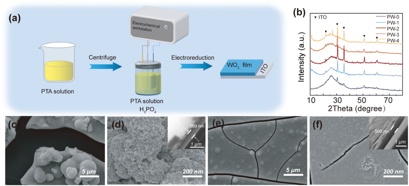 | ||
| Fig. 1 (a) Schematic diagram of the formation process for the P-doped amorphous WO3 films by a three-electrode system. (b) XRD patterns of the films. SEM images of (c and d) the PW-0 film and (e and f) the PW-2 film (insets: cross-sectional SEM images of the films). | ||
According to Fig. 2(a), W, P, and O are uniformly distributed throughout the PW-2 film, which is in agreement with the EDX spectra (Fig. S2c†). The phosphorus content of the five films is gradually increasing, which confirms the successful doping of phosphorus into the samples (Fig. S2a–e†). According to the TEM images and SAED pattern in Fig. 2(b) and (c), the PW-2 film is composed of small nanograins with a size distribution of 4.0–8.0 nm, HRTEM image and SAED pattern show an amorphous granular appearance, and no obvious structure is observed, particularly SAED pattern displays wide rings. Furthermore, XPS measurements of the PW-2 film are also used to confirm its chemical composition and valence state. As shown in the XPS survey spectrum, W, O, P, In, and C elements are present in the PW-2 film (Fig. S2e†). By using the C 1s binding energy (BE) as the reference, high-resolution XPS spectra of W 4f, O 1s, and P 2p peaks of the PW-2 film are shown in Fig. 2(d)–(f). The peaks of W 4f could be deconvoluted into W 4f5/2 and W 4f7/2 at 37.7 eV and 35.6 eV, which can be assigned to W6+ of the PW-2W film.26 In O 1s spectra, two peaks at 530.6 eV and 532.6 eV are relevant to the O–W and O–C bonds.27,28 For the P 2p spectra, the peak can be divided into three peaks, the peak at 133.6 eV refers to the P–O bond, while the peak at 130.2 eV belongs to the P–W,29,30 indicating the doped P atoms are almost in the PW-2 film, matched with the results detected by EDS.25
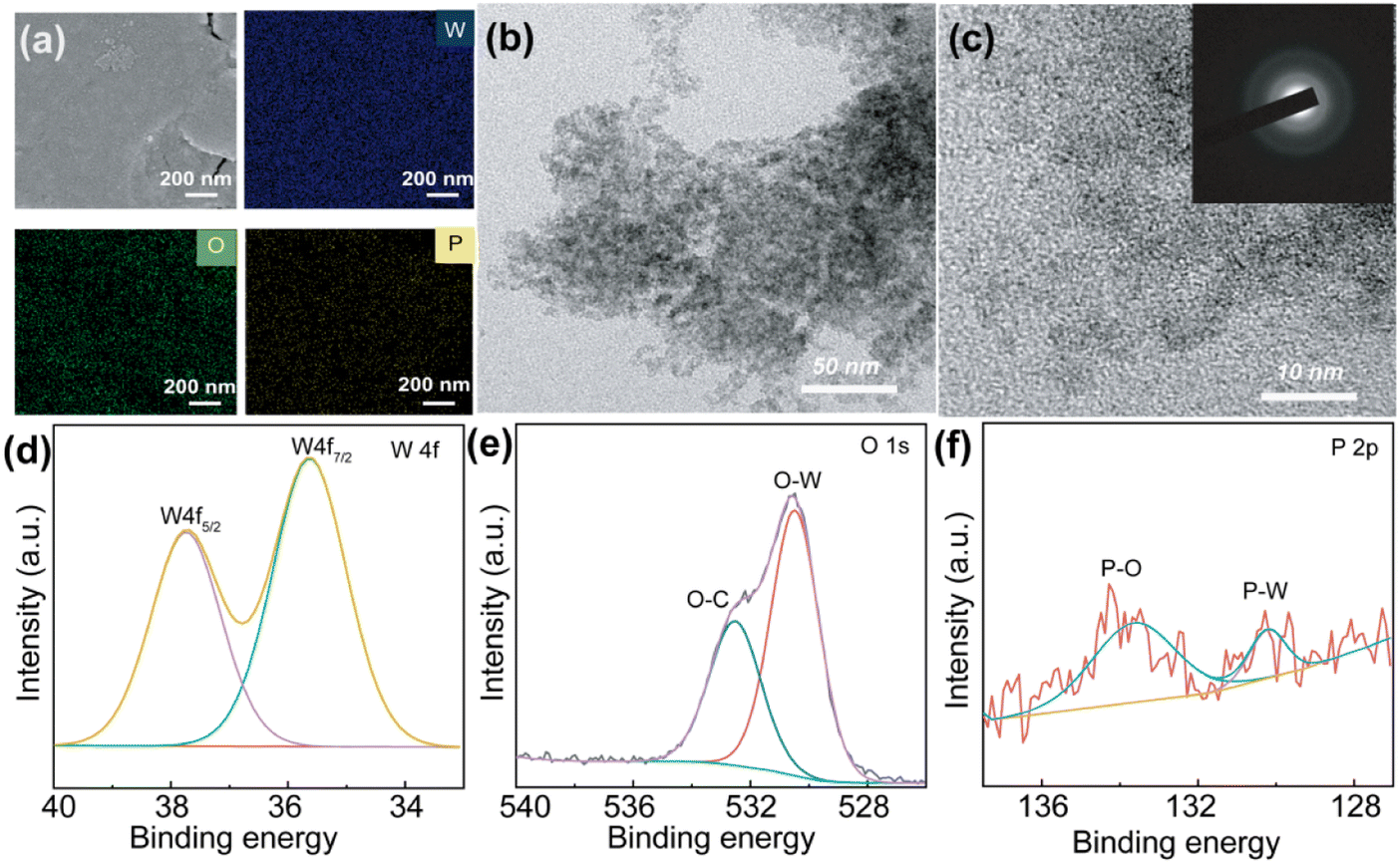 | ||
| Fig. 2 (a) EDS mapping images of the PW-2 film. TEM image (b) and HRTEM image (c) of the PW-2 film (inset: SAED pattern of the PW-2 film). High-resolution XPS spectra of W 4f (d), O 1s (e), and P 2p (f) peaks of the PW-2 film. | ||
The electrochemical and electrochromic properties of the P-doped WO3 films are evaluated in 1 mol L−1 LiClO4/PC, as shown in Fig. 3 and ESI.† Fig. 3(a) and S3(a)† exhibit the cyclic voltammogram (CV) of the P-doped amorphous WO3 films at a scan rate of 60 mV s−1, the electrochromic properties of the films are closely related to the area and the peak current of the CV. Among the P-doped amorphous WO3 films, the PW-2 film possesses the highest current and the largest area, which could show excellent electrochromic properties. The area and the peak current of the PW-3 film decrease significantly, showing the amount of added phosphoric acid is not the more the better, the PW-4 film further supports the results. After 200 cycles, the PW-2 film displays good cycle stability and high current density, while the PW-0 film has peeled off in this process, and the area of the PW-0 film becomes very small. Fig. 3(b) shows the transmittance spectra of the PW-0 and PW-2 films under a potential of ±1 V, the PW-2 film has a larger optical modulation (ΔT = 80.8% at 550 nm) due to cathodic coloration upon Li+ ion intercalation, the inset picture displays the colored and bleached states, while the PW-0 film only shows 32.7%, and the optical modulation of the PW-1, PW-3 and PW-4 films are 76.7%, 68.5% and 21.4% (Fig. S3b–d†).
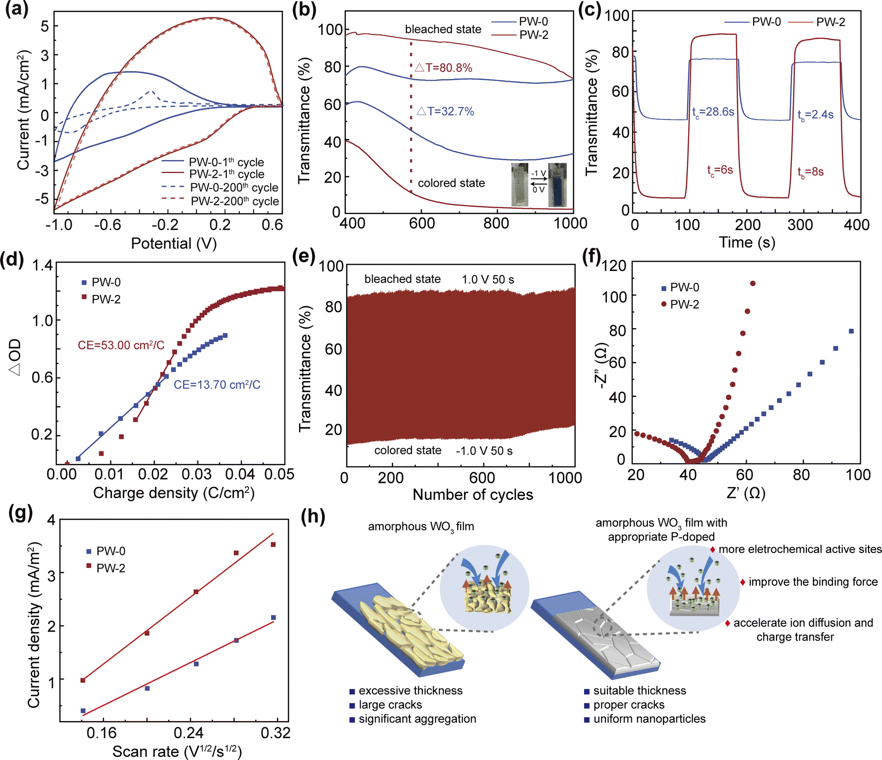 | ||
| Fig. 3 (a) Cyclic voltammograms of the P-doped amorphous WO3 films at a scan rate of 60 mV s−1 in 1 M LiClO4/PC. (b) Transmittance spectra of the P-doped amorphous WO3 films in colored state at −1 V and bleached state at 1 V. (c) The response times of the P-doped amorphous WO3 films. (d) Optical density vs. the charge density of the P-doped amorphous WO3 films at 550 nm with a potential of −1.0 V. (e) Cyclic stability of the PW-2 films tested by chronoamperometry for 1000 cycles. (f) Nyquist diagrams of the P-doped amorphous WO3 films at the frequency of 10 Hz to 105 Hz. (g) The cathodic peak current as a function of the square root of scanning rate for the P-doped amorphous WO3 films. (h) Scheme of the action mechanism of the P-doped amorphous WO3 films. | ||
The PW-0 film is loss of electrochromic function after 10 cycles under the alternating potential of ±1 V with 100 s per step, the optical modulation disappears due to the detachment of the film, and the PW-2 film still has excellent optical modulation (Fig. S4†). P-doped amorphous WO3 films are analyzed separately at 550 nm, where response times are defined as the time to reach 90% of the transmittance modulation. According to Fig. 3(c) and S5,† the coloration time (tc) and bleaching time (tb) of the PW-2 film are 6.0 s and 8.0 s, faster than the PW-0 film (tc = 28.4 s, tb = 2.4 s), the PW-1 film (tc = 25 s, tb = 6.0 s) and the PW-3 film (tc = 8.0 s, tb = 10.0 s). The PW-4 film is less stable than the PW-0 film, and the response times cannot be obtained. As a pivotal parameter to evaluate the electrochromic material, the CE relates the charge-per-unit-area to the change in optical density (OD), which can be calculated as follows.
 | (1) |
There are several reasons why the PW-2 film exhibits outstanding electrochromic properties (Fig. 3(h)). (1) The appropriate amount of P doping can improve the binding force, which dramatically enhances the stability of the film (Fig. 1 and S1†). (2) The surface of the PW-2 film possesses the proper cracks, the cracks ensure the integrity of the film, meanwhile the efficiency of the ion diffusion and charge transfer in the electrochromic process can be significantly improved, which leads to shorten the response times and increase the optical modulation. Fig. 3(f) and S7† depict the EIS spectra of the films, the PW-2 film shows the shortest semicircle radius, which indicates the lowest charge-transfer resistance. When the phosphoric acid dosage was too little or too much, the charge transfer rate of the film was slower. (3) Compared with the PW-0 film, P-doped induces the nanoparticles of the WO3 films more uniform without significant aggregation, as shown in Fig. 1(c)–(f), 2(a)–(c) and S1.† The nanoparticles not only can offer more electrochemical active sites, but also make ion diffusion and charge transfer more efficient. Calculating the Randles–Sevick equation based on voltammograms measured at different scan rates suggests that the intercalation/deintercalation of Li+ in the PW-2 film is easier than in the PW-0 film (Fig. 3(g)). At last, combining the inherent advantage of the amorphous phase, can greatly improve CE. Furthermore, Table S1† dislpays the electrochromic performance comparison with other previously reported works, which indicates the PW-2 film possesses excellent performance and has positive practical application.
An electrochromic device (ECD) is developed to evaluate the practical values in smart windows, especially for solar-heat regulation performance. The ECD is fabricated by the PW-2 film as the electrochromic layer, 1 mol L−1 LiClO4/PC as the electrolyte, as shown in Fig. 4(a). Fig. 4(b) and (c) display the electrochromic performance of the ECD, the ECD exhibits a reversible color-switching process at different potentials (1 V 100 s, −2.7 V 100 s), the optical modulation of the ECD reaches 77.0% at 550 nm (15.7% at colored state and 92.6% at bleached state) and 83.0% at 1000 nm (88.0% at colored state and 5% at bleached state), which presents wonderful visible light and near-infrared light shielding. To evaluate the solar-heat regulation performance, the ECD is embedded into a model house, and an electronic thermometer is used to record the temperature changes inside the model house, the colored and bleached states are shown in Fig. 4(d) at applied potentials of −2.7 V for 100 s and 1.0 V for 100 s, respectively. A xenon lamp source is used as the simulated solar light, and the temperature of the model house is about 28 °C before irradiation (Fig. 4(e)). When the light source illuminates the model house, the indoor temperature increases to 58 °C after 30 min of photo-irradiation under the bleached state, while the indoor temperature is only 47 °C in the colored state. The temperature difference is constant at 11 °C when the time is prolonged to 50 min, which validates the PW-2 film has excellent solar-heat regulation performance.
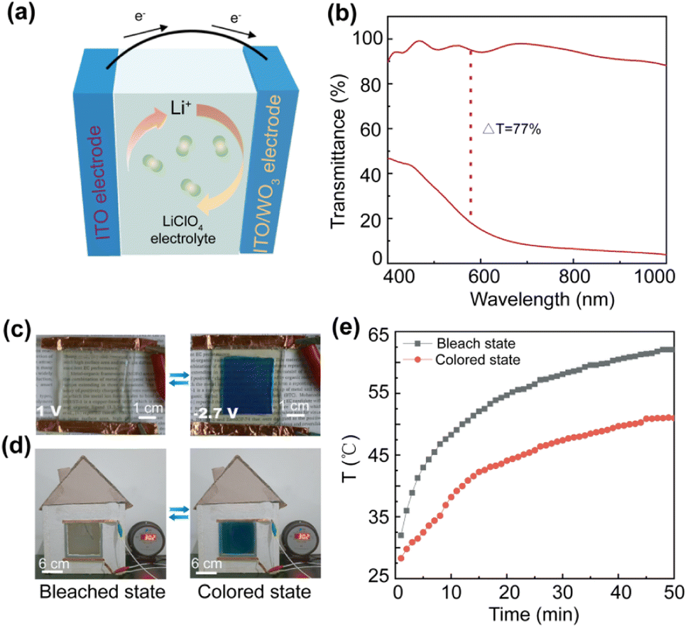 | ||
| Fig. 4 (a) Schematic illustration of the ECD structure. (b) Transmittance spectra of the ECD in the colored and the bleached states. (c) Digital images of the colored and bleached states of the ECD. (d) Photos of the colored and bleached states of the model house. (e) The temperature evolution of the model house over time in the colored and the bleached states. | ||
Conclusions
In summary, a series of P-doped amorphous WO3 films have been successfully prepared using the electrodeposition method. Among the P-doped amorphous WO3 films, the PW-2 film exhibits the most excellent electrochromic properties, which shows large optical modulation (80.8% at 550 nm), fast response times (6.0 s for coloration and 8.0 s for bleaching), high CE (53.00 cm2 C−1) and good cycling stability (1000 cycles). The mechanism of the outstanding electrochromic performance can be attributed to moderate P doping and amorphous, which can decrease the stress, improve the binding force, possess the proper cracks make the nanoparticles more uniform, and therefore accelerate the diffusion of ions and promote charge transfer dynamics. Moreover, the ECD which is fabricated by the PW-2 film, displays superb solar thermal regulation ability compared with the blank ITO. Finally, the ECDs fabricated by P-doped amorphous WO3 films have good prospects for application in electrochromic smart windows.Author contributions
Hongxi Gu: conceptualization, methodology and writing – original draft. Mengdi Tan: validation, investigation, formal analysis and data curation. Ting Wang: data curation and visualization. Jiayi Sun: data curation and visualization. Juan Du: formal analysis, visualization and writing – review & editing. Rong Ma: writing – review & editing and funding acquisition. Wei Wang: writing – review & editing and funding acquisition. Dengwei Hu: writing – review & editing and supervision.Conflicts of interest
The authors declare no competing financial interest.Acknowledgements
This work was supported by the National Natural Science Foundation of China (Grant No. 51902004), the Natural Science Basic Research Plan in Shaanxi Province of China (No. 2019JLM-48), the Youth Innovation Team of Shaanxi Universities, Shaanxi Provincial Education Department Foundation (No. 23JP003), Shaanxi Provincial Department of Education Special Scientific Research Project (Grant No. 22JK0244), the Key Research and Development Program of Shaanxi Province (No. 2021GY-159) and the Doctoral Scientific Research Starting Foundation of Baoji University of Arts and Sciences (No. ZK209010843).Notes and references
- C. Sui, J. Pu, T.-H. Chen, J. Liang, Y.-T. Lai, Y. Rao, R. Wu, Y. Han, K. Wang, X. Li, V. Viswanathan and P.-C. Hsu, Nat. Sustain., 2023, 6, 428–437 CrossRef.
- H. Zhai, D. Fan and Q. Li, Nano Energy, 2022, 100, 107435 CrossRef CAS.
- X. Li, W. Xie, C. Sui and P.-C. Hsu, ACS Mater. Lett., 2020, 2, 1624–1643 CrossRef CAS.
- M. N. Mustafa, M. A. A. Mohd Abdah, A. Numan, A. Moreno-Rangel, A. Radwan and M. Khalid, Renew. Sustain. Energy Rev., 2023, 181, 113355 CrossRef CAS.
- Y. Ke, J. Chen, G. Lin, S. Wang, Y. Zhou, J. Yin, P. S. Lee and Y. Long, Adv. Energy Mater., 2019, 9, 1902066 CrossRef CAS.
- Z. Zhang, L. Zhang, Y. Zhou, Y. Cui, Z. Chen, Y. Liu, J. Li, Y. Long and Y. Gao, Chem. Rev., 2023, 123, 7025–7080 CrossRef CAS PubMed.
- B. Deng, Y. Zhu, X. Wang, J. Zhu, M. Liu, M. Liu, Y. He, C. Zhu, C. Zhang and H. Meng, Adv. Mater., 2023, 35, 2302685 CrossRef CAS PubMed.
- S. Kandpal, T. Ghosh, C. Rani, A. Chaudhary, J. Park, P. S. Lee and R. Kumar, ACS Energy Lett., 2023, 8, 1870–1886 CrossRef CAS.
- T. Ghosh, S. Kandpal, C. Rani, A. Chaudhary and R. Kumar, Adv. Opt. Mater., 2023, 11, 2203126 CrossRef CAS.
- C. Gu, A.-B. Jia, Y.-M. Zhang and S. X.-A. Zhang, Chem. Rev., 2022, 122, 14679–14721 CrossRef CAS PubMed.
- S.-I. Park, Y.-J. Quan, S.-H. Kim, H. Kim, S. Kim, D.-M. Chun, C. S. Lee, M. Taya, W.-S. Chu and S.-H. Ahn, Int. J. Precis. Eng. Manuf.–Green Technol., 2016, 3, 397–421 CrossRef.
- C. C. Mardare and A. W. Hassel, Phys. Status Solidi A, 2019, 216, 1900047 CrossRef.
- D. Gao, H. Li, P. Wei, Y. Wang, G. Wang and X. Bao, Chin. J. Catal., 2022, 43, 1001–1016 CrossRef CAS.
- S. Aralekallu, R. Thimmappa, Z. M. Bhat, M. C. Devendrachari, N. C. Dargily, S. Mukhopadhyay, A. R. Kottaichamy and M. O. Thotiyl, ACS Sustain. Chem. Eng., 2021, 10, 259–266 CrossRef.
- M. Nemakal, S. Aralekallu, I. Mohammed, S. Swamy and L. K. Sannegowda, J. Electroanal. Chem., 2019, 839, 238–246 CrossRef CAS.
- S. Aralekallu, R. Thimmappa, P. Gaikwad, M. C. Devendrachari, A. R. Kottaichamy, S. P. Shafi, K. S. Lokesh, J. Sánchez and M. O. Thotiyl, ChemElectroChem, 2017, 4, 692–700 CrossRef CAS.
- V. H. V. Quy, I.-R. Jo, S.-H. Kang and K.-S. Ahn, J. Ind. Eng. Chem., 2021, 94, 264–271 CrossRef CAS.
- Y. Shi, M. Sun, Y. Zhang, J. Cui, Y. Wang, X. Shu, Y. Qin, H. H. Tan, J. Liu and Y. Wu, Sol. Energy Mater. Sol. Cells, 2020, 212, 110579 CrossRef CAS.
- Y. Zhang, X. Liang, T. Jiang, H. Liu, Y. Fu, D. Zhang and Z. Geng, Sol. Energy Mater. Sol. Cells, 2022, 244, 111820 CrossRef CAS.
- Z. Li, Z. Liu, L. Zhao, Y. Chen, J. Li and W. Yan, J. Alloys Compd., 2023, 930, 167405 CrossRef CAS.
- S. Xie, Z. Bi, Y. Chen, X. He, X. Guo, X. Gao and X. Li, Appl. Surf. Sci., 2018, 459, 774–781 CrossRef CAS.
- G. Gao, X. Tao, Y. He, Z. Li, J. Zhuang, L. He, Y. Li, Y. Wang, D. Sun and A. Xie, Appl. Surf. Sci., 2023, 640, 158346 CrossRef CAS.
- C. Sun, J. Zeng, H. Lei, W. Yang and Q. Zhang, ACS Sustain. Chem. Eng., 2018, 7, 1529–1537 CrossRef.
- A. Lelevic and F. C. Walsh, Surf. Coat. Technol., 2019, 369, 198–220 CrossRef CAS.
- G. Mineo, F. Ruffino, S. Mirabella and E. Bruno, Nanomaterials, 2020, 10, 1493 CrossRef CAS PubMed.
- H. Li, C. J. Firby and A. Y. Elezzabi, Joule, 2019, 3, 2268–2278 CrossRef CAS.
- R. Wang, W. Zhang, W. Zhu, L. Yan, S. Li, K. Chen, N. Hu, Y. Suo and J. Wang, Chem. Eng. J., 2018, 348, 292–300 CrossRef CAS.
- Y. Zhan, M. R. J. Tan, X. Cheng, W. M. A. Tan, G. F. Cai, J. W. Chen, V. Kumar, S. Magdassi and P. S. Lee, J. Mater. Chem. C, 2017, 5, 9995–10000 RSC.
- C. Sun, J. Zeng, H. Lei, W. Yang and Q. Zhang, ACS Sustain. Chem. Eng., 2018, 7, 1529–1537 CrossRef.
- K. Bon-Ryul, K.-H. Kim and H.-J. Ahn, Nanoscale, 2019, 11, 3318–3325 RSC.
Footnote |
| † Electronic supplementary information (ESI) available. See DOI: https://doi.org/10.1039/d4ra00979g |
| This journal is © The Royal Society of Chemistry 2024 |