DOI:
10.1039/D4RA00807C
(Paper)
RSC Adv., 2024,
14, 12897-12910
Tuning in optoelectronic properties of In/Te bilayer heterostructure upon annealing at different temperatures: surface wettability and photo response study for photonic and solar cell applications†
Received
31st January 2024
, Accepted 16th April 2024
First published on 22nd April 2024
Abstract
The current study depicted the influence of annealing temperature on In/Te bilayer thin film of 350 nm synthesized by thermal evaporation method. The interfacial diffusion of In into Te sites at different annealing temperatures (100 °C, 150 °C, 200 °C, 250 °C) modified the structural as well as the electro-optical response of the films. The structural study showed the appearance of an orthorhombic In4Te3 peak with annealing. The surface texture showed the particle nature with homogeneous distribution with annealing temperatures. The cross-sectional view of the bilayer and annealed film confirmed the formation of In/Te film with a total thickness of 350 nm. Surface mapping images confirm the homogeneous and uniform elemental distribution. The transmission was enhanced with annealing and showed broad transparency over the NIR region, making them suitable for IR device applications. The enhanced optical bandgap with annealing due to induced local structural changes reduced the optical parameters, such as refractive index, dielectric constant, and nonlinear susceptibility. The surface wettability measurements showed an enhanced hydrophobic nature with annealing. The variation of photocurrent with respect to voltage showed an ohmic nature, with enhancement from nA to ∼mA with annealing. Such alteration opened new ways to be used in solar cells, photodetectors, and photonic device applications.
1. Introduction
Multilayer and bilayer thin films have been studied extensively for designing different optoelectronic devices such as optical reflectors, solar cells, computer disks, and photodetectors.1–4 The intermixing among the layers in such multilayers and bilayer structures have profound technological significance. Different post-energy treatments on such thickness-dependent layers influence the materialistic properties due to diffusion among different layers. In this scenario, chalcogenide bilayer films are well known for creating a new type of nanocomposites that exhibited attractive optical and transport properties.5 For example, the effect of layer thickness and annealing temperature on In/Se bilayer film showed phase transition and increment in photocurrent absorption coefficient. This In/Se film structure is good as an absorber layer in hybrid solar cells.6 The annealing of Ag/In2Se3 bilayer film led to the appearance of AgIn5Se8 phase formation with an increment of optical bandgap due to phase transitions.7 Similarly, Sb/Ag2Se bilayer film with annealing reduced bandgap with transition from hydrophobic to hydrophilic nature in surface wettability study.8 In/Te bilayer film with thickness variation exhibited In2Te3 and In2Te5 phases. The grain size enhancement and bandgap energy reduction with film thickness have been observed.9 Similarly, in the aspect of dielectric and AC conductivity study, InTe bilayer films showed enhancement in capacitance with an increase in frequency at all temperatures. Such increment in capacitance might be attributed to charge carrier blocking at electrodes; thereby, the AC conduction is done by electronic hopping.10
In this aspect, the binary alloys from the III–VI group forming the chalcogenide semiconductors like Ga2Se3, In2Te3, InSe, In2S3, In2Se3, and so on have been largely studied for their useful applications as absorber layers in photovoltaic and photodetector applications.6,11 Indium telluride (InxTey) with direct bandgap energy is used in switching devices, pressure transducers, and gas sensors. There are various stable InxTey phases, like In2Te3, InTe, In4Te3, In3Te4, In7Te10, and In9Te11, with structural alteration in terms of α and β phase. The In4Te3, a P-type analogous of N-type In4Se3, exhibits anomalous thermal conductivity and is suitable for thermoelectric candidates in the mid-temperature regime. This material possesses an intrinsic narrow bandgap (<1 eV) and high photoelectronic output for infrared photons.12,13 It also exhibited strong anharmonicity in the low optical and acoustic regions. Such behavior originates from nonbonding and antibonding In4 valence electrons with their neighbours.14 Several studies related to this phase have been done.15–17 Li et al. investigated the anisotropic thermal and optical behaviours of In4Te3 and In4Se3 using theoretical models. High anisotropic optical changes were observed in the 0 to 10.0 eV energy range for In4Te3.15 Su et al. studied In4(Se1−xTex)3 in the doping aspect and concluded that negative magnetoresistance significantly enhanced with doping. The optical bandgap of In4Se2.7Te0.3 (0.55 eV) lies slightly higher than In4Se3 and In4Te3.17
Thermal annealing is a unique process in inducing crystallization and facilitating interdiffusion among layers. It is a process that modifies the material's surface texture with time at different temperatures. The relaxation condition of the material to its equilibrium state is faster by this thermal annealing process than the relaxation offered by conventional room temperature.18 Owing to its technological aspects, the effect of annealing on optical, electrical and structural behaviours of chalcogenide films has been investigated by several authors.19–21 Thus, by considering this aspect, In/Te films were annealed at different temperatures for the diffusion of In into Te to tune the optical, structural, morphology, and electronic properties.
The current work on bilayer In/Te heterostructure film annealed at various temperatures was studied for its structural change by Raman and X-ray diffraction (XRD). The contact angle measurement provides the surface wettability nature while the photo current–voltage response was recorded from the source measuring unit (SMU). The optical properties change was noticed from the UV-Visible data while the elemental confirmation was done by energy dispersive X-ray analysis (EDX). The film surface structure change due to annealing was imaged from a field emission scanning electron microscope (FESEM).
2. Synthesis and characterization procedure
The bilayer In/Te films of ∼350 nm thickness were prepared on clean glass substrate from 99.999% pure In and Te from Sigma-Aldrich by thermal evaporation method (Hind HiVac Smart Coat: 3.0 coating unit). Prior to deposition, the glass substrate was cleaned properly with diluted HNO3, aqueous NaOH, and distilled water. The substrates were dried at 100 °C inside a hot air oven. The bottom layer, Te, was deposited with a thickness of 300 nm, and then the In layer was sequentially deposited over it with a thickness of 50 nm under a 10−5 Torr vacuum at room temperature. So, the total thickness of the bilayer film was ∼350 nm, as monitored by the crystal thickness monitor. In situ quartz crystal thickness monitor monitored the thickness of the bilayer film. The prepared films were annealed at 100 °C, 150 °C, 200 °C and 250 °C for 1 h in vacuum oven presented in Scheme 1(a) having pressure 10−3 Torr, and the temperature gradient during annealing was ∼3–4 °C h−1.
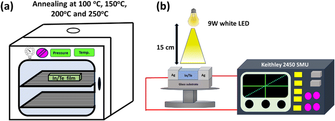 |
| | Scheme 1 The schematic presentation of In/Te bilayer thin film (a) annealed at 100 °C, 150 °C, 200 °C and 250 °C, (b) photo response measurement setup. | |
The structural study for the pristine In/Te and annealed films has been carried out using XRD (Bruker D8 Advances) with Cu Kα (wavelength = 1.54 Å) as the source and operating voltage at 30 kV and current of 40 mA. The scanning range was 20°–60° at a glancing angle of 1° and step size of 0.02° s−1, and scan speed of 1° min−1. The corresponding changes related to vibrational bonds have been analyzed by Raman spectral study (Horiba Raman spectrometer) by using a 632 nm He–Ne laser. The optical properties were studied by the JASCO-770 UV-Vis-NIR spectrophotometer, covering the wavelength range of 1200–2500 nm with a spectral resolution of 1 nm. The morphological analysis and determination of constituent element composition were performed by using JEOL, JSM-7601FPLUS FESEM with an attached EDX setup. The photo response studies of the films were conducted using the Keithley 2450 SMU. The surface wettability was tested using a DME-211 Plus contact angle measurement unit, which determines how effectively a liquid spreads or beads up on a surface and confirms the hydrophilic or hydrophobic nature of the films.
2.1 Photo response measurement
The photo response measurement of all the thin film samples was conducted by using Keithley 2450 SMU. For electrode purposes, the high-quality silver paste with an electrode area of 1 mm2 and a distance of 4 mm is applied at the edge of the sample after surface cleaning for conducting. The use of silver paste is very simple and shows good performance for electrical measurement. The prepared devices were carefully mounted on a sample holder for the measurement at room temperature (in Scheme 1(b)). A 9 W white LED light has been employed in order to cover the whole visible spectrum for illumination purposes. The light was illuminated through the exposed square of area 5 mm × 5 mm. The Keithley 2450 SMU was used for photocurrent measurement by varying voltage from −5 V to +5 V with step size 0.03 V at illumination conditions. The I–V measurements at four different spots were conducted to avoid measurement artifacts from the electrodes, and results are still inconsistent, indicating good electrode uniformity for I–V measurements. For each thin film sample, photocurrent measurements were carried out repeatedly for each of the five cases to confirm the consistent nature of the devices in this proper experimental setup. In order to create an isothermal condition and avoid direct heating of the sample due to the illumination, the sample was kept at an illumination distance of 15 cm used in our experiment.
3. Results and discussion
3.1 Structural analysis
Fig. 1(a) presents the In/Te films XRD pattern both in as-grown and annealed form. The prominent diffraction peaks at 23.03°, 27.56°, and 38.34° correspond to the (100), (101), and (012) planes of the hexagonal crystal system of tellurium (Te). In the as-grown bilayer film, the thickness of Te film is 300 nm, and In layer thickness is 50 nm. The greater thickness of tellurium compared to indium led to the dominant Te peaks, so no peaks corresponding to indium (In) have been observed. Such behaviour has been observed in other literature.22,23 Additionally, small peaks at 32.94°, 40.47°, 43.42° and 49.71° presented the In4Te3 orthorhombic crystal system having planes (520), (110), (122) and (332), respectively. However, with annealing, such significant peak shifting is observed except peak at 27.56° to 27.31°, which corresponds to the In4Te3 orthorhombic crystal system. Such shifting to a lower angle might be due to the annealing-induced lattice expansion. The average crystallite size, number of crystallites per unit area, dislocation density, and strains in lattice were determined from the XRD data by the Scherrer equation and related formula given by;24| |
 | (1a) |
Here, full-width half maxima (FWHM) β is in radians, wavelength of Cu Kα-line (λ = 1.54 Å), Bragg's angle is θ. The structural broadening is calculated as;25| |
 | (1b) |
where βexp and βstd refer to the integral X-ray peak profile width of the sample and the standard silicon reference. The other associate structural parameters of the films were evaluated as,26| |
 | (1c) |
| |
 | (1d) |
Here ‘d’ represented thickness of film (∼350 nm). Table 1 presents the calculated structural parameters and its error values that show the slight enhancement of crystallite size with annealing condition. This is possibly for the coalescence of grains in the sample. The sufficient heat energy through annealing is enough to enhance the interaction at the interface of In/Te bilayer film. Thus, the intense In4Te3 binary phase became more prominent with the appearance of smaller related peaks with temperature. This interaction led to more heteropolar In–Te bonds formed by breaking homopolar Te–Te bonds from the interface to the material medium. Therefore, disorder and defect reduction occur inside the band structure system by enhancing the bandgap. In another way, thermal annealing causes diffusion of one component in a bilayer film across the interface to increase, resulting in layer intermixing and the formation of more phases, as well as increased crystallinity of the material. Such small changes in average crystallite size could be attributed to a variety of factors, including the coherent volume of diffraction peaks, the thickness of the polycrystalline film, or the size of the grains. The film thickness is the same across all samples.27 The crystalline peaks that appeared in the annealed bilayer film had almost the same coherent volume of diffraction peaks as the as-grown film. However, with annealing, some small intensity extra peaks appeared, as well as a significant shift in the major peaks. This results in such a small change in crystallite size. On the other way, the strain in lattices and dislocation density is reduced by ensuring crystallinity enhancement. The annealing results in an increase in the grain boundary and reduces the lattice dislocation. The Nc value is reduced with temperature due to local structural change and crystallinity growth.
 |
| | Fig. 1 (a) XRD (b) Raman data for as-grown and annealed In/Te bi-layered thin film. | |
Table 1 Structural parameters for annealed In/Te bilayer films
| Samples |
D (nm) |
δ (nm−2) |
ε |
Nc (nm−2) |
| As-grown |
21.98 ± 0.05 |
0.0021 |
0.0054 |
0.0329 |
| 100 °C annl |
22.23 ± 0.04 |
0.0020 |
0.0053 |
0.0318 |
| 150 °C annl |
23.64 ± 0.09 |
0.0017 |
0.0052 |
0.0264 |
| 200 °C annl |
24.37 ± 0.02 |
0.0016 |
0.0051 |
0.0241 |
| 250 °C annl |
25.26 ± 0.08 |
0.0015 |
0.0046 |
0.0216 |
The room temperature Raman spectra analysis for both annealed and as-grown In/Te bilayer film were recorded in the range of 100–300 cm−1 and presented in Fig. 1(b). It showed two strong prominent peaks at 118 and 138 cm−1, corresponding to A1 and E2 modes of Te–Te vibration.28,29 These two peaks are consistent with annealing at different temperatures. However, these peak intensities are slightly varied with temperature, possibly due to the annealing-induced structural modification.30 The Raman spectra are deconvoluted and analysed by Gaussian contours with linear background subtraction, presented in Fig. S1(a)–(e),† to further study the structure of films. The deconvolution of as-grown Raman spectra showed the contribution from three individual peaks, in which primary two prominent peaks ascribed to A1 and E2 modes of Te–Te vibration. The intensity and sharpness of these peaks in all samples are contributed to the greater thickness of Te layer. The additional individual broad peak positioned at 154 cm−1, contributed to the Eg phonon vibration of the In–Te bond.31,32 However, the increase in the annealing temperatures clearly showed the increment in the broadness and intensity of this peak. This might be due to the annealing-induced diffusion, which results in the formation of more In–Te bonds, and this satisfied the XRD study.
3.2 Morphological study
The morphology of annealed and as-grown films is presented in Fig. 2. The FESEM images clearly showed the particle nature with homogeneous distribution. All the presented films showed a similar nature with not much changed surface morphology. However, the increased annealing condition led to the formation of small nanosheets on the surface. Such strong dependency of the surface morphology on annealing primarily affects the physical properties of the thin film. Morphological analysis of thin films becomes even more important in the perspective of bandgap and resistivity and for potential applications. The source of this structural difference might be factors of nucleation mechanisms, synthesis methods, crystal lattice stresses and activation energy.33 The particle size distribution for all films has been presented in Fig. 3. It showed a slight enhancement in the size with annealing, which was also observed from the XRD data of increased average crystallite size. The images clearly denote that all the film surfaces are well-coated structures. As the annealing temperature enhanced, the grains tend to agglomerate with each other to form bigger grains,6,9 which supported the XRD results.
 |
| | Fig. 2 FESEM images of (a) as-grown, (b) 100 °C, (c) 150 °C, (d) 200 °C, (e) 250 °C annealed In/Te bilayer thin films. | |
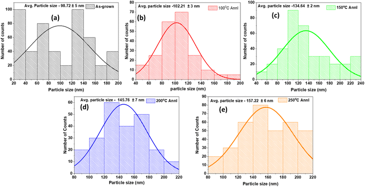 |
| | Fig. 3 Histogram showing the distribution of particles in films. | |
The EDX spectra for 150 °C annealed In/Te bi-layered film is presented in Fig. 4(a), confirming the presence of In and Te elements. The spectra have been taken over different regions to ensure homogeneity and uniformity over elemental compositions. The data presented in Table 2 for the elemental% in different conditions of the In/Te film clearly indicates the uniformity in elemental composition. Fig. 4(b)–(d) presents the 150 °C annealed film elemental mapping of In, Te, and both. The EDX and mapping have been taken at the same position for better elemental distribution clarity.
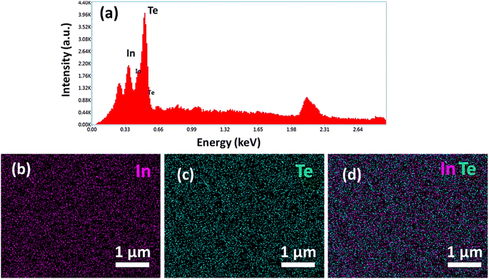 |
| | Fig. 4 (a) EDX spectra and Elemental mapping of (b) In, (c) Te, and (d) merged mapping of 150 °C annealed In/Te thin film. | |
Table 2 Elemental data of as-grown and annealed In/Te thin films
| Sample |
In/Te bilayer thin films |
| Temp. |
As-grown |
100 °C |
150 °C |
200 °C |
250 °C |
| Element |
Cal (at%) |
Obs (at%) |
Obs (at%) |
Obs (at%) |
Obs (at%) |
Obs (at%) |
| In |
14.28 |
14.11 |
14.22 |
13.90 |
14.25 |
14.29 |
| Te |
85.72 |
85.89 |
85.78 |
86.10 |
85.75 |
85.71 |
| Total |
100 |
100 |
100 |
100 |
100 |
100 |
Interface morphology of double-layered thin film as-grown and after annealing is presented in Fig. 5. Fig. 5(a) presents the as-grown In/Te bilayer structure with distinguishable layers showing the non-diffusion before annealing. The cross-sectional image shows the In layer (top layer) thickness as ∼39 nm while the Te layer (bottom) as ∼311 nm. The columnar growth of each layer is preferred in this case by stacking of adatom while film preparation. Fig. 5(b) presented a 250 °C annealed sample, which showed one layer with a thickness ∼350 nm. The annealing results in the diffusivity of the layers, which leads to the formation of a single layer. Moreover, the film becomes semicontinuous, which might be during sample deposition. This inhomogeneous nature mainly contributed to the small grains formed over the surface34 as observed from the SEM micrographs (Fig. 2(a)).
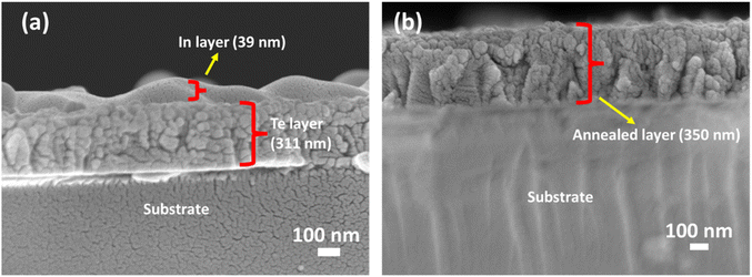 |
| | Fig. 5 Interface morphology of (a) as-grown (b) 250 °C annealed In/Te films. | |
3.3 Optical properties
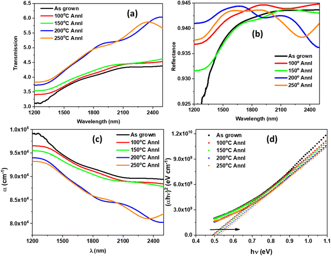
Fig. 6(a) infers the transmittance of both annealed and as-grown In/Te films over 1200–2500 nm wavelength. The transmission is found to be increased significantly for 200 °C, and 250 °C enhanced film, which could be due to the change in lattice defects concentration and localized state change over the gap region.35 In/Te bi-layered film showed greater transparency over the NIR range, which might be due to the free electron interaction with incident photons that led to a change in the polarization of light. Such interaction is responsible for the change in transmission over the IR region, which makes the material suitable for different IR applications such as IR lenses, fibers, and waveguides, including energy management, temperature detection, and monitoring, etc.36,37 The blue shift of absorption edge (towards lower wavelength) with annealing indicates the enhancement in the bandgap. The absorption edge of these films appeared between 1200–1800 nm. Fig. 6(b) shows the reflectance spectra of the films where the intensified reflectance peaks over the full IR region are observed. It showed a marked blue shift with annealing with the appearance of multiple reflectance peaks, which resulted from diffraction among different layers.
 |
| | Fig. 6 (a) Transmission, (b) reflectance (c) absorption coefficient variation with wavelength, (d) bandgap variation estimated by Tauc relation. | |
The absorption capability of a material is depicted by one optical parameter, namely, absorption coefficient (α). This parameter mainly plays a role in calculating the other related optical constants like bandgap, extinction coefficient (k), and skin depth (δ). The electronic transition between valence and conduction band also depends on ‘α’, which is estimated by using transmission and film thickness of the material as given by38
| |
 | (2) |
Here, the film thickness is denoted as ‘
t’, which is ∼350 nm. The change of ‘
α’ with ‘
λ’ is presented in
Fig. 6(c). The
α values are of the order of 10
4–10
5 cm
−1 over the IR range. However, it has been observed that the ‘
α’ reduced after the optical absorption edge, which signifies greater transparency at high wavelength range. The absorption coefficient showed a reduced pattern with annealing temperature.
The α ≥ 104 cm−1 regime is known as a high absorbance region, where conduction and valence band transition occur. It is also known as the Tauc region, which generally helps to estimate the bandgap energy, Eg, given by;39
Here, symbols like
ν,
h are having their usual meaning of frequency and Planck constant. The exponent ‘
m’ determines the nature of transition occurring in the sample called as transition factor. It also signifies the electron-density profile over valence and conduction bands. It is having different values like 1/2 and 3/2 for direct allowed and direct forbidden transition. The
m = 2 and 3 refer to the indirect allowed and forbidden transition case. The so-called Tauc parameter is denoted as
B, whose numerical value presents the degree of disorder in the bandgap regime. According to Mott and Davis's model, the crystalline material's fundamental absorption edge includes direct allowed transition, and amorphous material includes indirect allowed transition. The studied material showed a proper crystalline nature confirmed by the XRD pattern, so here
m = 1/2 has been considered for the bandgap estimation. The change in (
αhν)
2 vs. hν is shown in
Fig. 6(d), where the linear fitting of the data points led to the estimate of the optical bandgap. The slope determines the Tauc parameter ‘
B’ and the intercept on
X-axis measures the ‘
Eg’, value. The estimated
Eg and
B2 values for both films are presented in
Table 3. The
Eg showed an increasing trend with annealing temperature. This increase in
Eg is for annealing-induced change in the density of defect states over the forbidden gap region. Annealing is a well-known post-energy treatment that provides sufficient thermal energy for bond breaking, rearrangements, and reformations, resulting in the local structure change inside the matrix. Thus, this local structure change eliminates defects such as vacancy, interstitials, and dangling bonds.
40,41 This reduced the concentration of localized states enhanced the bandgap width. The band-tailing Tauc parameter presents the disorder magnitude inside the system. The value is decreased with annealing, as found in
Table 3. The increase in bandgap with top layer Se diffusion into the bottom As
2S
3 nanolayered film structure is due to the bond rearrangements with light energy and formation of new bonds of Se with As.
42 The decrease in strain due to the atomic motion of In into Te sites and change in local bonds to form In
4Te
3 phase brings down the absorption coefficient like the case of Se/As
2S
3 bilayer structure.
Table 3 Estimated optical entities for as-grown and annealed In/Te thin films
| Optical parameters |
As-grown |
100 °C annl |
150 °C annl |
200 °C annl |
250 °C annl |
| Optical bandgap (Eg) in (eV) |
0.491 |
0.496 |
0.517 |
0.524 |
0.530 |
| Tauc parameter (B2 × 1010) (cm−2 eV−2) |
1.893 |
1.877 |
1.852 |
1.8251 |
1.769 |
| Static linear refractive index (n0) |
4.140 |
4.129 |
4.081 |
4.066 |
4.053 |
| High-frequency lattice dielectric constant (ε∞ = n02) |
17.146 |
17.050 |
16.659 |
16.534 |
16.428 |
| χ(1) in esu |
1.285 |
1.277 |
1.246 |
1.236 |
1.228 |
| χ(3) × 10−10 esu |
4.643 |
4.533 |
4.107 |
3.977 |
3.871 |
| n2 × 10−9 esu |
4.225 |
4.136 |
3.791 |
3.685 |
3.598 |
| Optical electronegativity |
1.575 |
1.577 |
1.581 |
1.583 |
1.584 |
The skin depth (δ) is the path distance where the incident radiation intensity is reduced to 1/e value during its movement inside the sample. It is calculated as 1/α, i.e., reciprocal of α.36 The change of ‘δ’ as a function of energy is presented in Fig. 7(a), which shows the reduction of δ with hν. The thermal energy input led to an increase in the skin depth in the bilayer film. Similarly, the material's optical density (OD) is related to the absorption ability of the material during its exposure to electromagnetic radiation. It is estimated by the product of absorption coefficient and film thickness,43 i.e., OD = α × t. Fig. 7(b) presents the OD variation with hν, which changes like α.
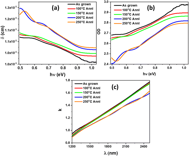 |
| | Fig. 7 Variation of (a) skin depth, (b) optical density as a function of energy, and (c) extinction coefficient for different In/Te films. | |
The refractive index is a crucial entity that plays a vital role in device fabrication and gives information related to transmitted electromagnetic wave velocity through the medium. It is generally presented by ñ = n + ik. The real part is denoted as ‘n’ while the imaginary part is associated with ‘k’. The real part relates to the light beam velocity propagating through the medium, and the imaginary part relates to the deterioration of the light beam while traversing. The value of ‘k’ was estimated from α and λ as given by,44  The estimated k as a function λ is shown in Fig. 7(c), which depicts a reduction with annealing temperature. The k is reduced and saturates at higher λ over the IR region. This behavior generally contributed from α, as α is low and transmission is high at higher wavelength, so the ‘k’ is lowest. It also means that there is no loss of incident radiation at the IR region, making it suitable for IR applications. The change in ‘k’ also tends to affect the nonlinearity of the material.
The refractive index (n) at hν → 0, namely static refractive index (n0) can be estimated for all synthesized samples from the ‘Dimitrov and Sakka empirical formula’,45
| |
 | (4) |
The estimated values of n0 for all samples by considering bandgap values are given in Table 3. The estimated amount showed an enhancement with the increase in annealing. Similarly, the real dielectric constant has been evaluated by using the relation, εL = (n0)2. The estimated real dielectric constant is presented in Table 3, which shows the same pattern as the static refractive index.
The nonlinear concept contributed to application in modern optical communication systems, ultrafast optical switching devices, optical telecommunication, parametric amplification, supercontinuum generation, optical processing, Raman amplification, etc. This behavior occurs while the polarization of the material responds in a non-linear manner toward electromagnetic waves falling on it. The linear polarization is lost in case of high-intensity radiation interaction on the sample, and in that case, polarization varies with the multi-power of electric field. This modifies the induced polarization (P) vector by series expansion in terms of applied electric field (E) and susceptibility (χ) as follows,46
| | |
P = ε0[χ(1)·E + χ(2)·E2 + χ(3)·E3 +…]
| (5) |
with linear polarization as ‘
χ(1)’ and the rest parts contributed to nonlinear response. However, for centrosymmetric media, the 2nd order nonlinear susceptibility becomes zero due to absence of inversion symmetry. So, the major contribution towards nonlinear phenomena are governed by the 3rd order nonlinear susceptibility (
χ(3)) in many semiconducting materials. The values of both
χ(1) and (
χ(3)) was calculated as,
47,48| |
 | (6) |
with ‘
A’ as constant factor of ∼1.7 × 10
−10 and no as the static refractive index.
Table 3 infers the reduced value of both ‘
χ(1)’ and ‘
χ(3)’ upon annealing condition. Such changes could be for the homogenization and polymerization due to annealing which led to local change in structure. This brings down the carrier concentration. The increase in ‘
Eg’ with simultaneous decrease in
χ(3) is shown in
Fig. 8 at different annealing temperatures.
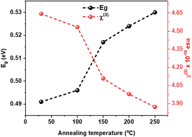 |
| | Fig. 8 Change in Eg and χ(3) with annealing temperature. | |
The quantity Δn (change in refractive index) originates from the nonlinear response as given by Δn = n2|E|2, where ‘n2’ as nonlinear refractive index and ‘E’ as applied electric field.49 The n2 for the as-grown and annealed films were determined through Ticha and Tichy and Miller's formula by,43,48  and tabulated in Table 3. It is reduced with annealing, for the decrease in defect states by annealing that reduced local polarizabilities.50 The electronegativity of the as-grown and annealed bilayer films has been estimated as,
  with ‘C’ as a constant (C = 25.54). It showed increment order with annealing, which might be due to an increase in the interaction at the interface of the bilayer film.
3.4 Surface wettability
The tuning of material surface by controlling the surface wettability is crucial for a lot of applications. For practical applications, both hydrophilic and hydrophobic materials are particularly desirable.51 Here, the annealing-induced surface wettability change for all samples is presented in Fig. 9. The measurements showed that all films showed a hydrophobic (θc > 90°) nature in Table 4; however, the hydrophobic nature enhanced with annealing. The contact angle measurement directly relies on the materials the local inhomogeneity, surface morphology and various chemical composition present in the sample texture. Here, annealing led to change the surface composition by interdiffusion among In and Te which might be a possible reason of such transition. However, the dominant effect for such surface wettability change mainly comes from the surface roughness variation induced by the annealing process. The increase in the hydrophobicity proves the rough and less compact of the material surface. Wenzel and Cassie–Baxter's models described the connection between surface morphology and wettability. Wenzel's model (cos![[thin space (1/6-em)]](https://www.rsc.org/images/entities/char_2009.gif) θw = rwcosθ) demonstrates the wettability of rough surface composed of small voids that inhibit water molecules and present strong adhesive forces between the water droplet and coatings.52 Conversely, as per Cassie–Baxter model, the air trapping between the liquid and solid surface affects the surface roughness. For smooth surface, the air trapping between liquid and solid is less whereas it is more for the rough surface.53 Hence, the rough surface observed from FESEM images (Fig. 2) mainly contributed to the hydrophobic nature. The observed increase in the contact angle attributed to the increase in the particle size and surface roughness, and reduced water absorption due to increased crystallinity during annealing. According to previous reports, with the annealing, the increment of contact angle of deposited bilayer also credited to the varying crystallinity.52 Here, water droplets spread over less area of the film surface, which will be an eligible candidate for self-cleaning and coating for solar cells, and photodetector device applications to improve durability.54,55
θw = rwcosθ) demonstrates the wettability of rough surface composed of small voids that inhibit water molecules and present strong adhesive forces between the water droplet and coatings.52 Conversely, as per Cassie–Baxter model, the air trapping between the liquid and solid surface affects the surface roughness. For smooth surface, the air trapping between liquid and solid is less whereas it is more for the rough surface.53 Hence, the rough surface observed from FESEM images (Fig. 2) mainly contributed to the hydrophobic nature. The observed increase in the contact angle attributed to the increase in the particle size and surface roughness, and reduced water absorption due to increased crystallinity during annealing. According to previous reports, with the annealing, the increment of contact angle of deposited bilayer also credited to the varying crystallinity.52 Here, water droplets spread over less area of the film surface, which will be an eligible candidate for self-cleaning and coating for solar cells, and photodetector device applications to improve durability.54,55
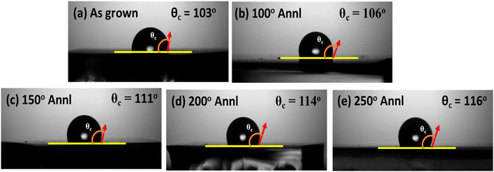 |
| | Fig. 9 Contact angle images of all studied samples. | |
Table 4 Work of adhesion and surface energy for the investigated films
| Samples |
θc (degree) |
Surface energy (γ) |
Work adhesion (Wsl) |
| As-grown |
103 |
57.16 |
128.30 |
| 100 °C annl |
106 |
51.18 |
121.41 |
| 150 °C annl |
111 |
40.63 |
108.16 |
| 200 °C annl |
114 |
47.20 |
116.58 |
| 250 °C annl |
116 |
69.95 |
141.93 |
The surface free energy (γ) of these as-grown and annealed In/Te thin films was calculated by,56
| |
 | (7) |
with
γw = 71.99 mN m
−1 (surface tension of water). The observed
γ values are presented in
Table 4. It showed an overall enhancement in surface energy. It played a significant part to known interfacial behavior during adhesion and wetting. Similarly, surface adhesion (
Wsl) is calculated by following Young–Dupre's equation, given as,
57| | |
Wsl = γw(1 + cosθ)
| (8) |
with
Wsl as the work of adhesion between the liquid and solid surfaces, and
γw as the surface tension between liquid and air interface. The estimated
Wsl is given in
Table 4, which infers an increment with annealing. It provides details on the molecular attention among solid surface and water drops. The annealing led to an increase in the binding strength between the film and water drop surface. Such change in surface wettability could be for surface roughness variation induced by the annealing process.
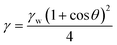
3.5 Photo response study
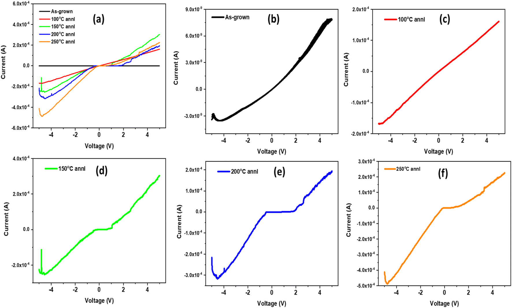
Fig. 10 represents the photo response curve of In/Te thin films annealed at different temperatures. The white light of 9 Watt has been employed with Keithley 2450 Unit over −5 V to 5 V range with a step size of 0.01 at room temperature. For conducting contact, a little amount of silver paste is layered at the two parallel edges of the films. The current variation with respect to voltage showed an ohmic nature. However, from Fig. 10(a) the photocurrent enhanced from nA to ∼mA by increasing in annealing temperature. This might be due to the reduction of defects and disorder inside the system. Annealing provides sufficient thermal energy for bond breaking, rearrangements, and reformations, resulting in elimination of defects inside the matrix by allowing the easy flow of electron through the medium.58,59 Generally, the high crystallinity with uniform grains improves the photo response in any semiconducting materials. Here, enhancement in crystallite size with annealing might be an important factor for increment of photocurrent. Additionally, the annealing induced electronic changes inside the film brings tuning in response of the charge carries at applied fields. Consequently, change in electronic moments improves the carrier mobility and conductivity of the material.59 Such behavior has also been observed in other literature.58–60 There is no significant change observed in the repeated I–V data of the thin film samples (Fig. S2(a)–(e)†). This shows high consistency nature of the all-thin films under light conditions, emphasizing the suitability for device applications.
 |
| | Fig. 10 Photo response of (a) all samples at light condition, photocurrent of (b) as-grown (c) 100 oC annl (d) 150 oC annl (e) 200 oC annl (f) 250 oC annl film. | |
Furthermore, the resistance of all films has been estimated from the inverse slope of the current–voltage plot (Fig. 11). It showed strong dependency over annealing temperature. The estimated resistance values are presented in Table 5. It showed a reduction of resistance inside the system with annealing, which might be due to lessening the defect state's density, which reduces the recombination and enhances the mobility.61,62
 |
| | Fig. 11 Resistance evaluation from current–voltage plot for (a) as-grown (b) 100 oC annl (c) 150 oC annl (d) 200 oC annl (e) 250 oC annl film. | |
Table 5 Estimated resistance values for all studied films
| Samples |
As-grown |
100 °C annl |
150 °C annl |
200 °C annl |
250 °C annl |
| Resistance (Ω) |
0.481 × 10⁹ |
0.298 × 10⁵ |
0.169 × 10⁵ |
0.158 × 10⁵ |
0.135 × 10⁵ |
4. Conclusion
In the present study, In/Te bilayer thin films were sequentially deposited by the thermal evaporation method, having a total thickness of 350 nm. The bilayer as-grown thin films were thermally annealed at distinct temperatures. The detailed structural study done by XRD and Raman spectroscopy showed the development of In4Te3 orthorhombic phase with higher annealing temperatures. The formation of particle structure was confirmed from morphological study with the increment of particle size with annealing. The cross-section of the film showed the distinct layers before annealing and intermixed with annealing. The transmission is enhanced with the reduction in the optical bandgap. This might be due to the annealing-induced diffusion at the film interface, which caused local structural changes. The nonlinear susceptibility and refractive index were reduced with annealing. The hydrophobicity is confirmed for all films, which can be an eligible candidate for self-cleaning and coating for solar cells and photodetector device applications to improve durability. The photocurrent variation with voltage confirmed ohmic nature with an increment from nA to ∼mA with annealing. These modifications opened pathways for solar cells, photodetectors, and photonic device applications.
Data availability
The data that support the findings of this study are available from the corresponding author upon reasonable request.
Author contributions
P. P.: writing of the original draft, software, experiment, data curation, and investigation. P. C.: experiment, data curation. R. N.: conceptualization, methodology, review and editing, and supervision.
Conflicts of interest
The authors declare no competing financial interest and also no conflicts of interest for this manuscript.
Acknowledgements
The author Dr R. Naik thanks the central instrumentation facility of ICT-IOC for different characterizations.
References
- M. Khan, K. A. Bhatti, R. Qindeel, F. Aleem, N. Rehman and N. Alonizan, Sol-gel deposition and characterization of multilayer 2% Cu doped TiO2 nano structured thin films, J. Mater. Sci.: Mater. Electron., 2017, 28, 9471–9477 CrossRef CAS.
- M. I. Khan, S. Imran, Shahnawaz, M. Saleem and S. U. Rehman, Annealing effect on the structural, morphological and electrical properties of TiO2/ZnO bilayer thin films, Results Phys., 2018, 8, 249–252 CrossRef.
- J. Kim, K. Barmak, M. D. Graef, L. H. Lewis and D. C. Crew, Effect of annealing on magnetic exchange coupling in CoPt/Co bilayer thin films, J. Appl. Phys., 2000, 87, 6140–6142 CrossRef CAS.
- J. I. Tani and H. Ishikawa, Fabrication and analysis of Mg3Bi2 thin films by post annealing Mg/Bi bilayer thin films, Mater. Lett., 2023, 331, 133460 CrossRef CAS.
- K. L. Naidu and M. G. Krishna, Effect of thermal annealing on disorder and optical properties of Cr/Si bilayer thin films, Philos. Mag., 2014, 94, 3431–3444 CrossRef.
- P. Matheswaran, R. S. Kumar and R. Sathyamoorthy, Effect of annealing on the structural and optical properties of InSe bilayer thin films, Vacuum, 2011, 85, 820–826 CrossRef CAS.
- R. Panda, R. Naik and N. C. Mishra, Thermal annealing induced evolution of AgIn5Se8 phase from Ag/In2Se3 bilayer thin film, J. Alloys Compd., 2019, 778, 819–826 CrossRef CAS.
- S. Das, S. Paikaray, I. Swain, S. Senapti and R. Naik, Tuning in linear and nonlinear optical parameters by interfacial mixing of Sb/Ag2Se bilayer thin films under annealing at different temperatures for optoelectronic applications, Surf. Interfaces, 2023, 42, 103395 CrossRef CAS.
- P. Matheswaran, B. Gokul, K. M. Abhirami and R. Sathyamoorthy, Thickness dependent structural and optical properties of In/Te bilayer thin films, Mater. Sci. Semicond. Process., 2012, 15, 486–491 CrossRef CAS.
- P. Matheswaran, E. Sathyamoorthy, R. Sravanakumar and S. Velumani, AC and dielectric properties of vacuum evaporated InTe bilayer thin films, Mater. Sci. Eng., B, 2010, 174, 269–272 CrossRef CAS.
- H. Lan, L. Wang, Y. Li, S. Dang, Y. Yue, T. Zhang, S. Zhang, M. Zeng and L. Fu, Self-modulation-guided growth of 2D tellurides with ultralow thermal conductivity, Small, 2022, 18, 2204595 CrossRef CAS PubMed.
- M. O. Sorokatyi, V. M. Strebezhev, I. M. Yuriychuk, S. V. Nichyi and V. G. Pylypko, Structural, optical and photoelectric properties of crystals and heterostructures based on the In4Se3, In4Te3, and In4(Se3)1-x(Te3)x semiconductors, 2022 IEEE 41st International Conference on Electronics and Nanotechnology (ELNANO), Kyiv, Ukraine, 2022, pp. 128–132 Search PubMed.
- T. A. Melnychuk, V. M. Strebegev and G. I. Vorobets, Laser synthesis of thin layers of In4Se3, In4Te3 and modification of their structure and characteristics, Appl. Surf. Sci., 2007, 254, 1002–1006 CrossRef CAS.
- A. Das and P. Banerji, Antibonding or nonbonding interaction-driven phonon modes softening and wave-like interband thermal conduction in layered In4Te3 under the framework of wigner transport formalism, ACS Appl. Energy Mater., 2023, 6(22), 11521–11531 CrossRef CAS.
- X. Li, B. Xu, G. Yu, L. Xue and L. Yi, Anisotropic optical and thermoelectric properties of In4Se3 and In4Te3, J. Appl. Phys., 2013, 113, 203502 CrossRef.
- F. L. Faita, K. Ersching, J. J. S. Acuna, C. E. M. Campos and P. S. Pizani, Structure and microstructure of In4Te3 nano-powders prepared by solid state reaction, Mat, Chem. Phys., 2011, 130, 1361–1365 CAS.
- W. Su, S. Zhao, L. Li and D. Hua, Optical properties and low temperature magnetoresistance of In4 (Se1− xTex) 3 alloy, J. Alloys Compd., 2014, 587, 560–564 CrossRef CAS.
- P. Priyadarshini, D. Sahoo, A. Aparimita, D. Alagarasan and R. Ganesan, Switching of linear and nonlinear optical parameters in As35Se65 thin films upon annealing at both above and below Tg, Appl. Phys. A, 2020, 126, 910 CrossRef CAS.
- S. A. Khan, J. K. Lal and A. A. Al-Ghamdi, Thermal annealing effect of on optical constants of vacuum evaporated Se75S25−xCdx chalcogenide thin films, Opt. Laser Technol., 2010, 42, 839–844 CrossRef CAS.
- R. Naik, A. Aparimita, D. Alagarasan, S. Varadharajaperumal and R. Ganesan, Linear and nonlinear optical properties change in Ag/GeS heterostructure thin films by thermal annealing and laser irradiation, Opt. Quantum Electron., 2020, 52, 136 CrossRef CAS.
- S. Pech, Y. J. Rou, S. Kim, K. Y. Lee and N. H. Kim, Cu(In,Ga)Se2:Te thin films for stoichiometric compensation by using co-sputtering and rapid thermal annealing, Appl. Sci., 2023, 13(7), 4284 CrossRef CAS.
- Y. Wang, B. Li, L. Huang, H. Cao, L. Zhao and N. Ren, Effect of Ag layer thickness and scan line spacing during laser annealing of Ag/F-doped SnO2 bilayer composite thin films under ultrasonic vibration assistance, J. Alloys Compd., 2020, 829, 154504 CrossRef CAS.
- R. K. Mangal and Y. K. Vijay, Study of annealing effects in In–Sb bilayer thin films, Bull. Mar. Sci., 2007, 30, 117–121 CAS.
- E. R. Shaaban, Optical constants and fitted transmittance spectra of varies thickness of polycrystalline ZnSe thin films in terms of spectroscopic ellipsometry, J. Alloys Compd., 2013, 563, 274–279 CrossRef CAS.
- E. R. Shaaban, I. S. Yahia, N. Afify, G. F. Salem and W. Dobrowolski, Structural and the optical dispersion parameters of nano-CdTe thin film/flexible substrate, Mater. Sci. Semicond. Process., 2014, 19, 107–113 CrossRef CAS.
- P. Priyadarshini, S. Das, D. Alagarasan, R. Ganesan, S. Varadharajaperumal and R. Naik, Role of bismuth incorporation on the structural and optical properties in BixIn35-xSe65 thin films for photonic applications, J. Am. Ceram. Soc., 2021, 104, 5803–5814 CrossRef CAS.
- B. J. Jena, D. Alagarasan, R. Ganesan and R. Naik, Thermal annealing induced linear/nonlinear properties of Ag2S/As2Se3 heterojunction films for optoelectronic applications, Ceram. Int., 2023, 49(16), 27535–27550 CrossRef CAS.
- Q. Luo, G. Tang, M. Sun, G. Qian, Q. Qian and Z. Yang, Single crystal tellurium semiconductor core optical fibers, Opt. Mater. Exp., 2020, 10, 1072–1082 CrossRef CAS.
- S. Khatun, A. Banerjee and A. J. Pal, Nonlayered tellurene as an elemental 2D topological Insulator: experimental evidence from scanning tunneling spectroscopy, Nanoscale, 2019, 11, 3591–3598 RSC.
- S. Das, P. Priyadarshini, D. Alagarasan, S. Vardharajperumal, R. Ganesan and R. Naik, Structural, morphological, and linear/non-linear optical properties tuning in Ag60-xSe40Tex films by thermal annealing for optoelectronics, J. Non-Cryst. Solids, 2022, 592, 121742 CrossRef CAS.
- V. Rajaji, K. Pal, S. C. Sarma, B. Joseph, S. C. Peter, U. V. Waghmare and C. Narayana, Pressure induced band inversion, electronic and structural phase transitions in InTe:A combined experimental and theoretical study, Phys. Rev. B: Condens. Matter Mater. Phys., 2018, 97, 155158 CrossRef CAS.
- S. Misra, C. Barreteau, J. C. Crivello, V. M. Giordano, J. P. Castellan, Y. Sidis, P. Levinsky, J. Hejtmanek, B. Malaman, A. Dauscher, B. Lenoir, C. Candolfi and S. Pailhes, Reduced phase space of heat-carrying acoustic phonons in single-crystalline InTe, Phys. Rev. Res., 2020, 2, 043371 CrossRef CAS.
- O. Kahveci, A. Akkaya, E. Yucel, R. Aydın and B. Sahin, Production of p-CuO/n-ZnO:Co nanocomposite heterostructure thin films: An optoelectronic study, Ceram. Int., 2023, 49, 16458–16466 CrossRef CAS.
- X. Cen, A. M. Thron, X. Zhang and K. van Benthem, Cross-sectional characterization of the dewetting of a Au/Ni bilayer film, Ultramicroscopy, 2017, 178, 131–139 CrossRef CAS PubMed.
- E. R. Shaaban, Optical constants and fitted transmittance spectra of varies thickness of polycrystalline ZnSe thin films in terms of spectroscopic ellipsometry, J. Alloys Compd., 2013, 563, 274–279 CrossRef CAS.
- S. Mishra, P. L. Singh and D. K. Dwivedi, Thin film preparation and optical properties of Se–Te based chalcogenide glasses for optoelectronic applications, Glass Phys. Chem., 2020, 46, 341–349 CrossRef.
- F. Charpentier, B. Bureau, J. Troles, C. B. Pledel, K. Michelle-Le Pierres, F. Smektala and J. L. Adam, Infrared monitoring of underground CO2 storage using chalcogenide glass fibers, Opt. Mater., 2009, 31, 496–500 CrossRef CAS.
- M. Behera, N. C. Mishra, R. Naik, C. Sripan and R. Ganesan, Thermal annealing induced structural, optical and electrical properties change in As40Se60-xBix chalcogenide thin films, AIP Adv., 2019, 9, 095065 CrossRef.
- J. Tauc, Optical Properties of Amorphous Semiconductors, Springer, 1974, pp. 159–220 Search PubMed.
- M. A. Abdel-Rahim, M. M. Hafiz and A. Z. Mahmoud, Influence of thickness and annealing on optical constants of Se82. 5Te15Sb2. 5 chalcogenide thin films, Solid State Sci., 2015, 48, 125–132 CrossRef CAS.
- F. S. Al-Hazmi, Effect of annealing on optical constants of Se75S25− xCdx chalcogenide thin films, Phys. B, 2009, 404, 1354–1358 CrossRef CAS.
- K. V. Adarsh, R. Naik, K. S. Sangunni, S. Kokenyesi, H. Jain and A. C. Miller, Kinetics and chemical analysis of photoinduced interdiffusion in nanolayered Se/As2S3 films, J. Appl. Phys., 2008, 104(5), 053501 CrossRef.
- D. Sahoo, P. Priyadarshini, A. Aparimita, D. Alagarasan, R. Ganesan, S. Varadharajaperumal and R. Naik, Optimization of linear and non-linear optical parameters of As40Se50Te10 thin films by thermal annealing, Opt. Laser Technol., 2021, 140, 107036 CrossRef CAS.
- M. A. Alvi, A. A. Al-Ghamdi and J. H. Madani, Synthesis and characterization of Bi doped Se–Te nanostructured thin films, Measurement, 2014, 58, 325–329 CrossRef.
- V. Dimitrov and S. Sakka, Linear and non-linear optical properties of simple oxides, J. Appl. Phys., 1996, 79(3), 1741–1745 CrossRef CAS.
- L. Benjamin, P. Dube, C. B. Tabi and C. M. Muiva, Physical, linear and nonlinear optical properties of amorphous Se90-xTe10Mx (M = Zn, In, Pb, x = 0, 5) chalcogenide thin films by electron-beam deposition, J. Non-Cryst. Solids, 2021, 557, 120646 CrossRef CAS.
- H. Ticha and L. Tichy, Semiempirical relation between nonlinear susceptibility (refractive index), linear refractive index and optical gap and its application to amorphous chalcogenides, J. Optoelectron. Adv. Mater., 2002, 4, 381–386 CAS.
- S. Mishra, P. K. Singh, R. K. Yadav, A. Umar, P. Lohia and D. K. Dwivedi, Investigation of glass forming ability, linear and nonlinear optical properties of Ge–Se–Te–Sb thin films, Chem. Phys., 2021, 541, 111021 CrossRef CAS.
- A. S. Hassanien and I. Sharma, Optical properties of quaternary a-Ge15-xSbxSe50Te35 thermally evaporated thin-films: refractive index dispersion and single oscillator parameters, Optik, 2020, 200, 163415 CrossRef CAS.
- A. S. Hassanien, Studies on dielectric properties, opto-electrical parameters and electronic polarizability of thermally evaporated amorphous Cd50S50−xSex thin films, J. Alloys Compd., 2016, 671, 566–578 CrossRef CAS.
- C. Nefzi, B. Yahmadi, N. E. Guesmi, J. M. Garcia, N. K. Turki and S. A. Ahmed, A successful exploitation of gamma-radiation on chalcogenide Cu2InSnS4 towards clean water under photocatalysis approach, J. Mol. Struct., 2022, 1251, 131943 CrossRef CAS.
- Z. Ahmad, C. Xu, T. Shahid, M. Arfan and Z. Song, Vacuum annealing effects on the microstructure and properties of HfO2-based bilayer antireflective coatings by magnetron sputtering, Vacuum, 2023, 215, 112241 CrossRef CAS.
- J. Y. Wang, W. H. Li, Z. Wei, C. Zhang, Y. H. Li, G. Xu and S. Q. Zang, A hydrophobic semiconducting metal–organic framework assembled from silver chalcogenide wires, Chem. Commun., 2020, 56, 2091–2094 RSC.
- Y. Y. Quan and L. Z. Zhang, Experimental investigation of the anti-dust effect of transparent hydrophobic coatings applied for solar cell covering glass, Sol. Energy Mater. Sol. Cells, 2017, 160, 382–389 CrossRef CAS.
- T. Halenkovic, M. Baillieul, J. Gutwirth, P. Nemec and V. Nazabal, Amorphous Ge-Sb-Se-Te chalcogenide films fabrication for potential environmental sensing and nonlinear photonics, J. Mater., 2022, 8, 1009–1019 Search PubMed.
- P. Priyadarshini, A. Parida, D. Alagarasan, R. Ganesan and R. Naik, Time-dependent laser irradiation-induced kinetics of changes in linear-nonlinear optical properties of Bi15In20Se65 thin films for IR applications, J. Appl. Phys., 2023, 133, 063104 CrossRef CAS.
- A. B. Gurav, S. S. Latthe, R. S. Vhatkar, J. G. Lee, D. Y. Kim, J. J. Park and S. S. Yoon, Superhydrophobic surface decorated with vertical ZnO nanorods modified by stearic acid, Ceram. Int., 2014, 40, 7151–7160 CrossRef CAS.
- Anjali, B. S. Patial, S. Chand and N. Thakur, On high-field conduction and I–V measurements in quaternary Se–Te–In–Pb nano-chalcogenide thin films, J. Mater. Sci.: Mater. Electron., 2020, 31, 2741–2756 CrossRef CAS.
- D. Alagarasan, S. Varadharajaperumal, K. D. A. Kumar, R. Naik, A. Arunkumar, R. Ganesan, G. Hegde and E. E. S. Massoud, Optimization of different temperature annealed nanostructured CdSe thin film for photodetector applications, Opt. Mater., 2021, 122, 111706 CrossRef CAS.
- S. Das, S. Senapati, D. Alagarasan and R. Naik, Temperature dependent Raman and photoresponse studies of Bi2Te3 thin films annealed at different temperatures for improved optoelectronic performance, Mater. Adv., 2024 10.1039/D3MA01044A.
- A. Parida, S. Senapati, S. Samal, S. Bisoyi and R. Naik, One-pot hydrothermal synthesis of SnMnS nanosheets for dielectric energy storage applications, ACS Appl. Nano Mater., 2023, 6, 11230–11241 CrossRef CAS.
- M. Devika, N. K. Reddy, K. Ramesh, K. R. Gunasekhar, E. S. S. R. Gopal and K. T. R. Reddy, Low resistive micrometer-thick SnS : Ag films for optoelectronic applications, J. Electrochem. Soc., 2006, 153, 727 CrossRef.
|
| This journal is © The Royal Society of Chemistry 2024 |

 Open Access Article
 This Open Access Article is licensed under a Creative Commons Attribution-Non Commercial 3.0 Unported Licence
 ,
Prabhukrupa C. Kumar
,
Prabhukrupa C. Kumar


 The estimated k as a function λ is shown in Fig. 7(c), which depicts a reduction with annealing temperature. The k is reduced and saturates at higher λ over the IR region. This behavior generally contributed from α, as α is low and transmission is high at higher wavelength, so the ‘k’ is lowest. It also means that there is no loss of incident radiation at the IR region, making it suitable for IR applications. The change in ‘k’ also tends to affect the nonlinearity of the material.

 and tabulated in Table 3. It is reduced with annealing, for the decrease in defect states by annealing that reduced local polarizabilities.50 The electronegativity of the as-grown and annealed bilayer films has been estimated as,
  with ‘C’ as a constant (C = 25.54). It showed increment order with annealing, which might be due to an increase in the interaction at the interface of the bilayer film.