DOI:
10.1039/D4RA00433G
(Review Article)
RSC Adv., 2024,
14, 6656-6698
Perovskite materials in X-ray detection and imaging: recent progress, challenges, and future prospects
Received
17th January 2024
, Accepted 7th February 2024
First published on 22nd February 2024
Abstract
Perovskite materials have attracted significant attention as innovative and efficient X-ray detectors owing to their unique properties compared to traditional X-ray detectors. Herein, chronologically, we present an in-depth analysis of X-ray detection technologies employing organic–inorganic hybrids (OIHs), all-inorganic and lead-free perovskite material-based single crystals (SCs), thin/thick films and wafers. Particularly, this review systematically scrutinizes the advancement of the diverse synthesis methods, structural modifications, and device architectures exploited to enhance the radiation sensing performance. In addition, a critical analysis of the crucial factors affecting the performance of the devices is also provided. Our findings revealed that the improvement from single crystallization techniques dominated the film and wafer growth techniques. The probable reason for this is that SC-based devices display a lower trap density, higher resistivity, large carrier mobility and lifetime compared to film- and wafer-based devices. Ultimately, devices with SCs showed outstanding sensitivity and the lowest detectable dose rate (LDDR). These results are superior to some traditional X-ray detectors such as amorphous selenium and CZT. In addition, the limited performance of film-based devices is attributed to the defect formation in the bulk film, surfaces, and grain boundaries. However, wafer-based devices showed the worst performance because of the formation of voids, which impede the movement of charge carriers. We also observed that by performing structural modification, various research groups achieved high-performance devices together with stability. Finally, by fusing the findings from diverse research works, we provide a valuable resource for researchers in the field of X-ray detection, imaging and materials science. Ultimately, this review will serve as a roadmap for directing the difficulties associated with perovskite materials in X-ray detection and imaging, proposing insights into the recent status, challenges, and promising directions for future research.
1. Introduction
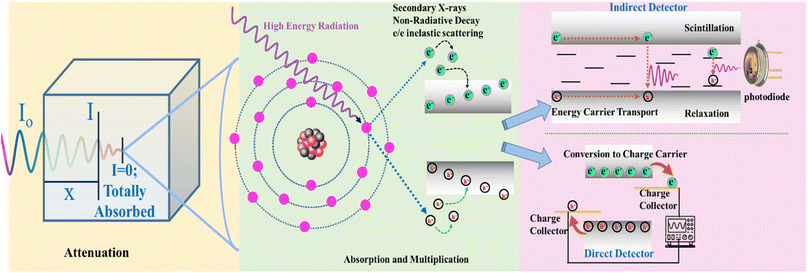
The sensing and imaging of high-energy ionizing radiation, particularly X-rays, is important for diverse applications including homeland security, national defense, medical imaging, sustainable energy, industrial monitoring, environmental surveys, non-destructive inspection, and fundamental scientific research.1,2 For example, X-ray computed tomography imaging has been widely utilized to examine lung infections linked with the COVID-19 disease, which aids in the comprehensive understanding of the disease.3–6 Solid-state semiconductor-based radiation detectors offer several benefits due to their unique properties and capabilities in the gas field, together with scintillating material-based high-energy radiation detectors such as X-ray detectors.7 Experimentally, it has been proven that 300![[thin space (1/6-em)]](https://www.rsc.org/images/entities/char_2009.gif) 000 electron–hole pairs are generated by 1 MeV energy in a semiconductor, which is about 10 times higher than the number of ion pairs generated by the same energy in a gas chamber.8 Consequently, it improves the signal-to-noise ratio in comparison with a pulse-type signal in an ion chamber. Besides this benefit, high-energy particles including alpha/beta can only traverse a short distance typically in the range of micrometers/millimeters, which would be a few centimeters/meters in gases at ambient pressure.9 This indicates that a relatively thin radiation detector can fully absorb the whole energy of the incident particle. During the penetration of high-energy particles in a semiconducting material, the energy loss to the valence band electron elevates at the conduction band by generating an electron–hole pair. In semiconductor detectors, an electric field is applied across the detector to drift the electrons and holes toward their respective electrodes, and the corresponding output signal is generated.10 The complete procedure is depicted in Fig. 1.
000 electron–hole pairs are generated by 1 MeV energy in a semiconductor, which is about 10 times higher than the number of ion pairs generated by the same energy in a gas chamber.8 Consequently, it improves the signal-to-noise ratio in comparison with a pulse-type signal in an ion chamber. Besides this benefit, high-energy particles including alpha/beta can only traverse a short distance typically in the range of micrometers/millimeters, which would be a few centimeters/meters in gases at ambient pressure.9 This indicates that a relatively thin radiation detector can fully absorb the whole energy of the incident particle. During the penetration of high-energy particles in a semiconducting material, the energy loss to the valence band electron elevates at the conduction band by generating an electron–hole pair. In semiconductor detectors, an electric field is applied across the detector to drift the electrons and holes toward their respective electrodes, and the corresponding output signal is generated.10 The complete procedure is depicted in Fig. 1.
 |
| | Fig. 1 Working principle of a radiation detector. | |
The effectiveness of X-ray detectors relies on the high sensitivity and detection efficiency of weak and high-energy X-rays. The performance of X-ray-detecting semiconducting materials is closely related to their average atomic number, charge carrier mobility, and carrier lifetime.11–13 To date, only a few compounds have been commercially employed for sensing and imaging X-ray radiation, including silicon (Si), amorphous selenium (α-Se), germanium (Ge), and cadmium zinc telluride (CdZnTe). However, these types of detectors have several drawbacks including low average atomic number, large leakage currents, low X-ray attenuation coefficient, high production costs, relative chemical toxicity, poor mechanical qualities, and increasing performance deterioration with time owing to the polarization effect.14 Thus, it is essential to explore new materials to replace the conventional materials for X-ray sensing and imaging.
A new class of materials known as perovskites has emerged, which is expressed by the stoichiometric formula ABM3, where A represents a monovalent inorganic/organic cation, B represents a divalent metal cation and M signifies a halide anion.15 The halogens can also be replaced by oxygen, nitrogen, or carbon. Usually, A and B are shown as divalent and tetravalent ions, respectively, with oxygen used for charge neutrality instead of halogen. To preserve the charge neutrality, the cubic perovskite structure is made up of corner-sharing BM6 octahedra, which produce a 3D network, where the A site cations reside in the 12-fold coordinated (cuboctahedral) vacancies. Alternatively, perovskite materials may be observed as a cubic close-packed AM3 sub-lattice comprised of divalent B-site cations inside the six-fold coordinated (octahedral) cavities.16
To date, these materials have shown promise in multifaceted applications with high efficacy such as photovoltaic solar cells, magnetic memory devices, gas sensing, bio-imaging, light-emitting diodes, and solid-state fuel cells.17–22 From 2009 onward, the photovoltaic research community has achieved an enhancement in the PCE from 3.81% to 25.8% by gaining a thorough grasp of the essential properties of perovskites and functional device approaches.23,24 In recent years, perovskite materials have appeared as new promising materials for ionizing radiation sensing owing to their exclusive benefits including high average atomic number Z (to absorb high-energy photons), appropriate bandgap energy, high resistivity, large mobility–lifetime product (a high capacity to gather carriers), low production cost, excellent charge carrier transportation properties, and outstanding tolerance to defects.25–30 The superior features of perovskite materials in comparison with other semiconducting materials used commercially are depicted in Fig. 2(a)–(e). This indicates why researchers have been attempting to use perovskite materials for radiation detection.
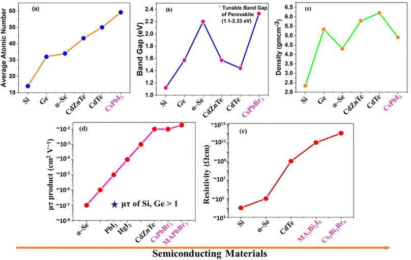 |
| | Fig. 2 Comparison of (a) atomic structure, (b) electronic behavior, (c) material characteristics, and (d and e) electrical properties of perovskite materials with different semiconducting materials for high-energy radiation detectors.31–39 | |
In this study, we provide a comprehensive review on X-ray detection directly by overviewing the evolution of perovskite materials, innovation and modification of their synthesis process with cost-effective techniques and the device architectural modification. In addition, we discuss the fundamental properties of materials and devices in regard to radiation detection and their working principle. Moreover, we discuss the potentiality of OIH perovskites, all-inorganic perovskites and lead-free perovskites as X-ray detectors. Finally, the existing problems associated with perovskites as X-ray detectors are discussed and the future possibility of research presented. The essence of our review work is depicted in Fig. 3.
 |
| | Fig. 3 Brief essence of this review. | |
2. Fundamentals of radiation detecting materials and devices
In this section, we focus on exploring the details of both material and device characteristics, with precise emphasis on the interdependence between them. The characteristics and features of devices are necessarily shaped by the innate properties of the materials employed. In the realm of material properties, we investigated aspects such as radiation attenuation ratio, ionization energy, and the mobility–lifetime product. In parallel, the discussion is extended to device-specific properties, covering parameters such as dark current, charge collection efficiency, sensitivity, limit of detection, and response time. This comprehensive exploration aims to explain the intricate relationship between material characteristics and the performance metrics of corresponding devices.
2.1. Radiation attenuation ratio
The attenuation of incident radiation occurs due to the interaction of incident radiation with materials through mainly Rayleigh scattering, photoelectric effects, Compton scattering, and pair production processes. This attenuation can be estimated by the Beer–Lambert law, which is expressed by eqn (1), as follows:| |
 | (1) |
where I represents the intensity of the attenuated radiation, Io indicates the initial intensity of incident radiation, μ denotes the linear attenuation coefficient, ρ signifies the density of the material and x symbolizes the distance radiation penetrates into the material. Researchers in the field of radiation use μ to compare the attenuation ability of numerous materials upon exposure to radiation. It gives information on how a material interacts with incident radiation. A higher value of μ for a material indicates its high ability to attenuate (more absorption) radiation. The linear attenuation coefficient in inverse length units can be expressed as follows (2):| |
 | (2) |
where Z indicates the atomic number of the material, A specifies the atomic mass and E represents the energy of the incident radiation. In addition, the mass attenuation coefficient is another way to predict a the attenuation capability of a material, which signifies the linear attenuation coefficient normalized by the density of the material. Consequently, a constant value is obtained for a specific element or compound. This constant value is a characteristic feature that helps to compare and quantify the ability of a material regarding radiation attenuation irrespective of its mass or thickness. In the case of direct detection, the ideal materials possess a high atomic number Z (>40) for completely absorbing incident radiation and converting it into electrical signals.40 This is consistent with halide perovskite materials from the aspect of the atomic number of their elements such as Pb, I, Cs, and Ag. Thus, perovskite materials possess higher atomic numbers in comparison with some conventional materials such as Si (Z = 14) and α-Se (Z = 34). It can be shown that under 50 keV X-ray photons, for completely absorbing this radiation, the required thickness of halide perovskite lies between the thickness of CZT and α-Se material. In brief, it can be said that a perovskite material with a high atomic number and moderate density is a promising candidate for radiation detection.41
The attenuation ratio, denoted by ε, of a material can be expressed with a thickness of L by eqn (3), as follows:
The number of photons absorbed per second by the material is defined by the absorption rate, which can be explained according to eqn (4), as follows:
| |
 | (4) |
where
D denotes the dose rate and
m represents the mass of material.
2.2. Ionization energy
The ionization energy is the amount of energy required to produce an electron–hole pair in a material. In the case of the majority of semiconducting materials, the ionization energy is solely related to their band gap and follows empirical formula (5):42where W denotes the ionization energy, Eg specifies the bandgap, and A and B are constants. According to the literature, this energy for most of the perovskite materials can be described by eqn (6), which is nearly an order of magnitude lower than the ionization energy of α-Se.43
When perovskites and amorphous selenium are exposed to the same dose of high-energy photons, perovskites produce an order of magnitude more electron–hole pairs in comparison with amorphous selenium. This suggests that perovskite materials are highly encouraging semiconductors as the absorbing layer in high-energy photon detectors.
2.3. Charge collection efficiency
The charge collection efficiency (CCE) represents the ratio of the total charge collected by the electrode to the total charge generated within a material when it is exposed to radiation. Alternatively, it can be defined as the measurement of how effectively a detector can convert incident radiation into a measurable electrical signal. A higher CCE signifies superior performance in terms of perfectly detecting and quantifying radiation. Theoretically, one can calculate the number of electron–hole pairs created by a high-energy photon using eqn (7).| |
 | (7) |
where β represents the highest number of radiation-generated carriers. These radiation-generated electron–hole pairs will drift toward their respective electrode under a bias and generate an electronic signal in the external circuit.
Theoretically, the maximum light-generated current (Ip) can be expressed by eqn (8), as follows:
where
e denotes the electronic charge. By considering the carrier loss due to recombination and trapping, the modified Hecht
eqn (9) can be adopted to estimate the actual photo-generation current accumulated by the electrodes.
44| |
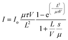 | (9) |
where
Io represents the saturated photocurrent,
L denotes the thickness of the material layer,
V signifies the bias voltage,
S indicates the surface recombination rate,
τ symbolizes the carrier lifetime and
μ stands for the carrier mobility. Now the charge collection efficiency (CCE) can be expressed by
eqn (10).
45| |
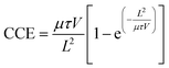 | (10) |
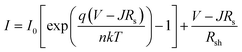
2.4. Dark current
The current–voltage relation for the single diode equation or the Shockley diode equation is given by (11), as follows:| |
 | (11) |
where n represents the ideality factor, I0 indicates the reverse saturated current, Rsh signifies the shunt resistance and Rs symbolizes the series resistance and k, T, and q represent the Boltzmann constant, temperature, and electronic charge, respectively. In the absence of light, the reverse saturated current is known as the dark current (Idark). In some electronic devices, particularly radiation detectors, this reverse saturation current can contribute to noise in the signal. A lower Idark value can result in devices with lower noise levels and improved sensitivity to weak optical signals. In addition, a lower value of Idark also contributes to better energy resolution by reducing the electronic noise. Normally, semiconducting materials with high resistivity display a low Idark in devices.46 In addition, halide perovskite materials retain high resistivity in the range of 107–1012 Ω cm, which is beneficial for high energy radiation detection especially for X-rays.37,47,48
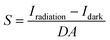
2.5. Sensitivity
Sensitivity in radiation detection refers to the capability of a radiation detector to efficiently detect radiation. The high sensitivity of a radiation detector is a key parameter because it can shorten the exposure time as well as reduce the risk of ionizing radiation. In addition, a highly sensitive radiation detector generates a substantial electronic signal when exposed to the same radiation and enhances its distinct identification capabilities. Typically, sensitivity is explained by the accumulation of charge per unit area under exposure to radiation. The sensitivity can be expressed by eqn (12).49| |
 | (12) |
where Iradiation/Idark, D, and A are the output current with/without X-ray irradiation, the X-ray irradiation dose rate and sensing area, respectively.
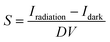
In addition, the sensitivity of a detector can also be expressed by eqn (13).50
| |
 | (13) |
where
V represents the volume of the detector. Moreover, the sensitivity of the device is influenced by the radiation attenuation, carrier extraction, electron–hole generation, and photoconductivity gain.
51
2.6. Limit of detection
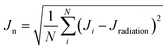
Noise influences the sensitivity and the LDDR of the detector via noise current. There are four types of noise current including shot noise (ishot), thermal noise (ithermal), generation–recombination noise (ig–r) and flicker noise  . The thermal and shot noise are frequency independent and called white noise. Alternatively, the generation–recombination and flicker noise are frequency dependent.52 In addition, it has been reported that large resistivity can reduce the shot noise, and a large band gap leads to low thermal noise.53 Thus, a high resistance and large band gap are criteria for materials that can be used as a detector. The International Union of Pure and Applied Chemistry (IUPAC) declared that the detection limit of the producing signal value is three times the noise54 and the scientific community employs a signal-to-noise ratio (SNR) value of three to describe the limit of detection in radiation detection, especially X-ray detectors.55 The SNR is expressed by eqn (14).56
| |
 | (14) |
| | |
Js = Jradiation − Jdark
| (14a) |
| |
 | (14b) |
where Js, Jn, Jradiation and Jdark indicates the signal current density, noise current density, photo-current density and dark current density, respectively. Two key factors (Jradiation and Jdark) that meaningfully influence the SNR are the introduction of carriers from both contact interfaces and the existence of thermally activated carriers within the intrinsic material.57
2.7. Mobility–lifetime product
The mobility (μ)–lifetime (τ) product of charge carriers is a central and crucial parameter that is employed to assess the quality and performance of extracting charge carriers from deep inside a material. It is directly correlated with the efficient collection of charge carriers produced by incident radiation. μτ can be obtained by fitting the data in the Hecht plot (9). Also, μτ is adopted to estimate the diffusion length of charge carriers using the eqn (15), as follows:| |
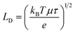 | (15) |
The diffusion length of holes,  (10–50 μm) is typically larger than that of electrons
  (1–5 μm).58 Thus, perovskite-based direct detectors function in hole collection mode. Generally, a longer diffusion length helps the carriers to accumulate at the respective electrode. In the case of radiation detectors, a longer LD is preferable because several millimeter-thick perovskite materials are used for completely absorbing high-energy radiation. Thus, the scientific community has attempted to increase LD by enhancing the bias voltage although it initiates the Idark, which hampers the device performance.59 In this case, by adopting a few modifications including structure design, optimized synthetic process and post-treatment, the μτ can be enhanced without initiating Idark. For an example, W. Pan and team increased the μτ from 3.75 × 10⁻³ cm2 V−1 to 6.3 × 10⁻³ cm2 V−1 for the SC structure of Cs2AgBiBr6 by adopting annealing post-treatment.60
2.8. Response time
The response time is employed to assess how quickly a detector can sense, which is distinguished as the required time for a photo-current rising from 10% to 90% of the saturated photo-current, and then falling from 90% to 10% of the saturated photo-current. Generally, the dropping time is larger than the rising time because it is closely related with the trap state and crystalline quality.61 For an example, Liu and group fabricated a perovskite-based X-ray detector using MA3Bi2I9 SCs and obtained a rising time and dropping time of 266 μs and 417 μs, respectively.62 In the case of an ideal radiation detector, a short response time is required, which lessens the exposure time to radiation and enables its usage in imaging including fluoroscopy.
3. Active layer fabrication techniques
3.1. Single crystal
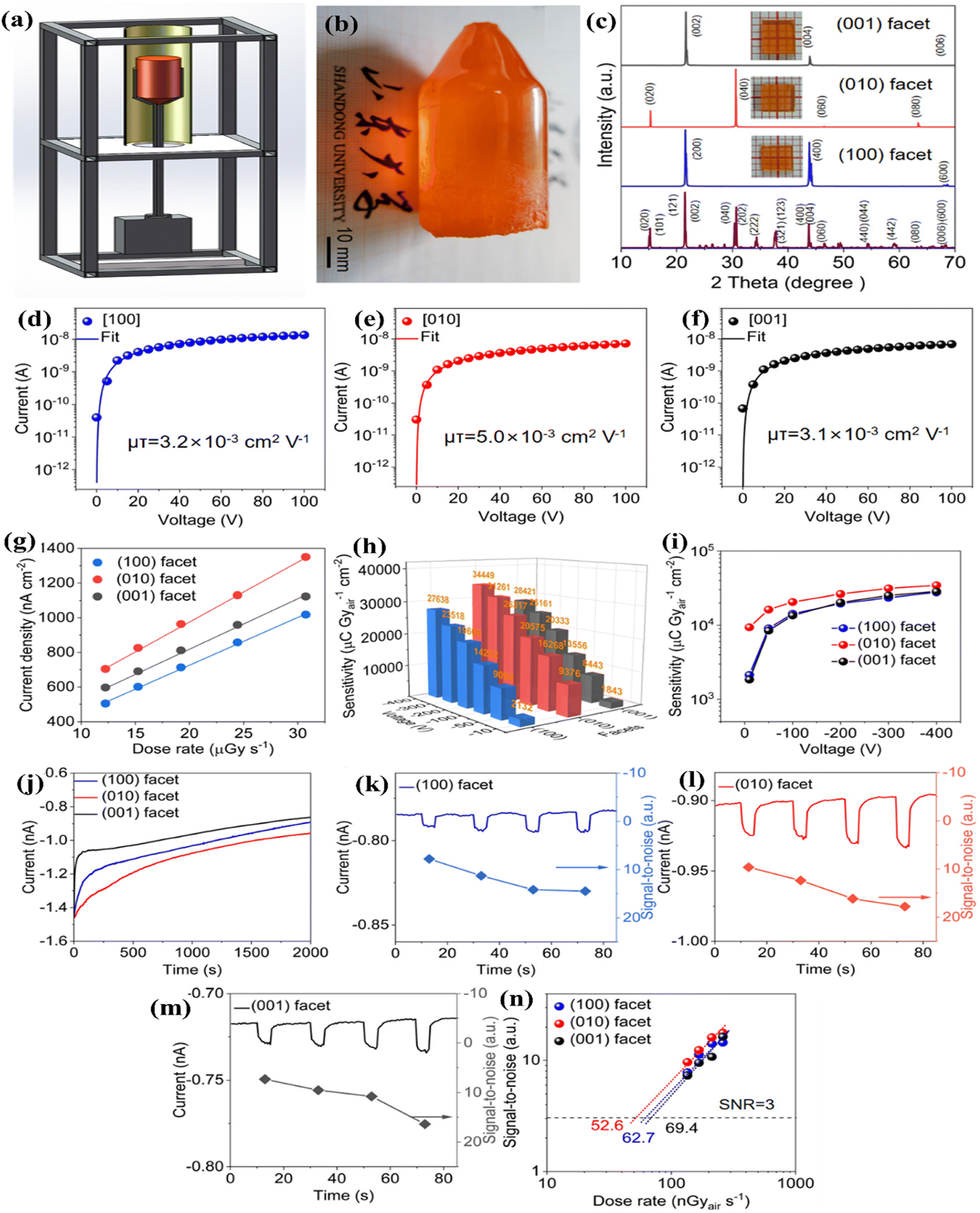
A renowned research team under the leadership of Jiayue Xu conducted a comprehensive overview of the recent progress in the crystal growth of metal halide perovskites.63 Their study discussed the challenges associated with controlling growth defects and improving the crystal quality and provided an understanding of the trap states and defects in the crystals. Their discussion comprehended the advantages of employing perovskite single crystals over polycrystalline thin films in optoelectronic devices. Furthermore, they scrutinized several studies where the authors asserted that perovskite single crystals display fewer defects, lack grain boundaries, and exhibit superior ambient stability in comparison to polycrystalline thin films.64 These attributes make high-quality perovskite single crystals more alluring for exploring their intrinsic physical properties and devising high-performance devices. As an illustration, they provided an example naming a trap density for a crystal (CsPbBr3) that is reported to be 5–6 orders of magnitude lower than that of its polycrystalline film counterparts.65 The majority of researchers used perovskite material-based SC structures for detecting high-energy radiation. Perovskite SCs are more beneficial in many ways such as they exhibit lower defects, lack of grain boundary scattering and offer lower intrinsic carrier concentration.66,67 Specifically, SC-based halide perovskite offers a large mobility–lifetime product, large diffusion length, and minimal Idark.68,69 These properties have a huge significance for rapid and efficient high-energy radiation detection. Since the early 2010s, the fascination has been growing with adopting organic SCs as active semiconducting materials in direct ionizing radiation detection. This attentiveness has been meaningfully boosted by the progress in solution-growth techniques by producing large, high-quality crystals.70,71 For instance, C. C. Stoumpos and team fabricated a perovskite-based radiation detector for the first time, where they obtained a large μτ product for holes, which was ten-times larger than that of the commercially available CZT.72 To date, many fabrication strategies have been adopted to synthesize large-scale perovskite-based SCs. These methods are described in the next subsection together with a schematic diagram.
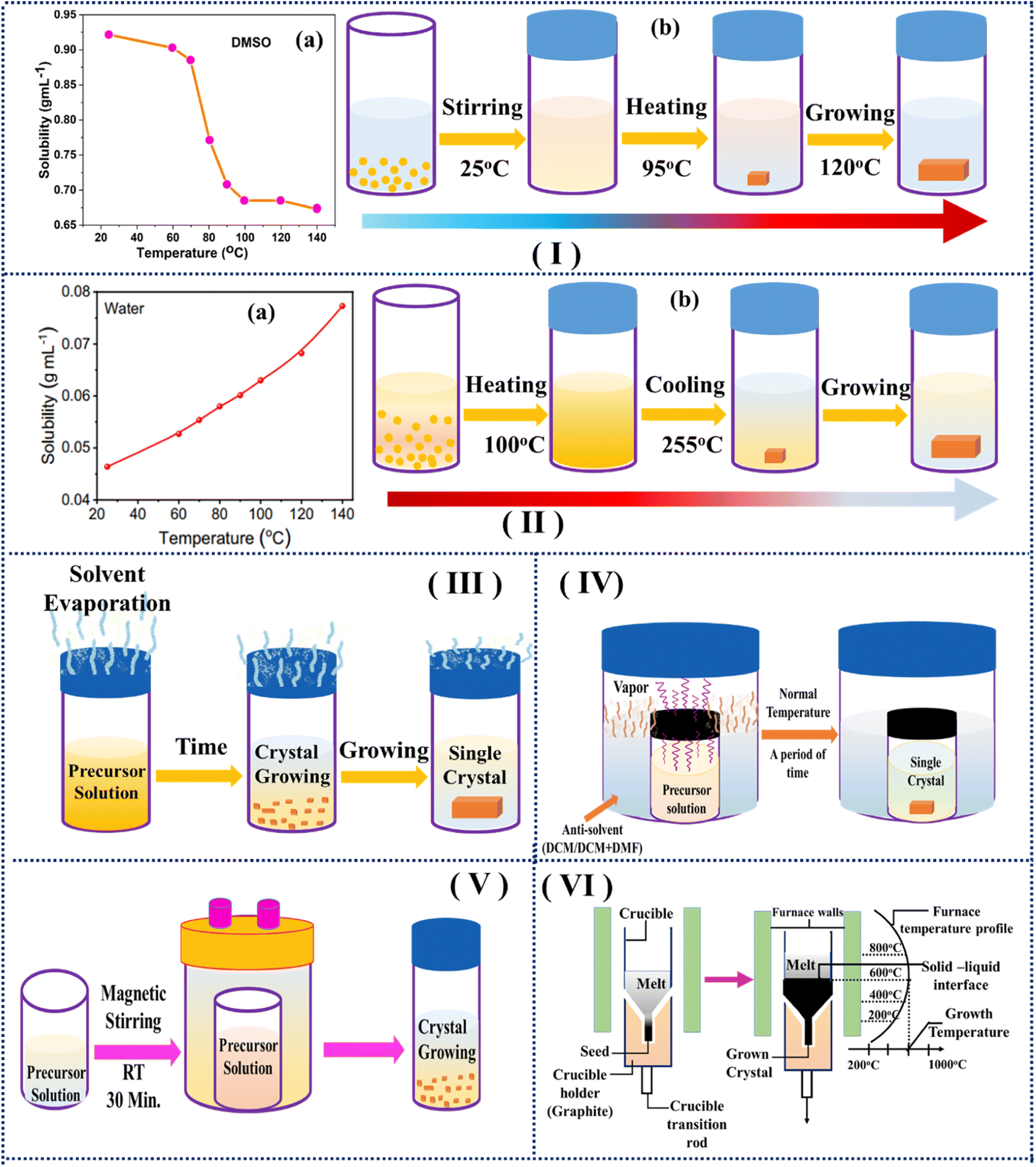
3.1.1. Inverse-temperature crystallization (ITC). ITC is considered a rapid crystal growth technique for obtaining high-quality, large-scale and controlled-shape perovskite SCs. It is also appropriate for materials that have high solubility at room temperature and low solubility at high temperature in particular solvents.73,74 In general, the solubility of a solute in a solvent decreases when the temperature of the solution or melt cools. Consequently, a crystal will be formed after the concentration of the solute exceeds its solubility limit. However, ITC exhibits the reverse scenario. In the ITC method, the solute is dissolved in the solvent at room temperature, and then the solution is gradually heated to reach a saturated state for growing SCs. Many researchers have adopted this ITC method to synthesize OIH perovskites such as MA3Bi2I9 and FAPbX3 (X = Cl, Br, I) and all-inorganic perovskites including Cs3Bi2I9.75,76 In the literature, we found that dimethyl sulfoxide (DMSO), N,N-dimethylformamide (DMF), and γ-butyrolactone (GBL) are used frequently as solvents in the growth of SCs. Recently some researchers used 3-(decyldimethylammonio)propanesulfonate inner salt (DPSI) as an additive to decrease the defect formation rate.77 A schematic illustration of the ITC method is depicted in Fig. 4I(a) and (b).78
 |
| | Fig. 4 Some promising SC growth methods: (I) (a) temperature-dependent solubility of CsPbBr3 in DMSO79 and (b) inverse temperature crystallization. (II) (a) Temperature-dependent solubility of CsPbBr3 in water79 and (b) temperature-lowering crystallization. (III) Solvent evaporation method; (IV) anti-solvent vapor-assisted method; (V) hydrothermal method; and (VI) Bridgman method. | |
3.1.2. Temperature-lowering crystallization (TLC). TLC is a straightforward method employed for the growth of the SC perovskite active layer. In this method, the solution is gradually cooled at a controlled rate, and thus the perovskite solution can be oversaturated, starting to form an SC. Using this TLC method, rubrene SCs were developed with a volume of 1 cm3, which were employed for neutron detection.80 In addition, X. Song and group fabricated large SCs of a metal-free halide perovskite named DABCO–NH4Br3 (DABCO = N-N′-diazabicyclo[2.2.2]octonium) by adopting the TLC technique, where the temperature of the solution was cooled at a rate of 5 °C/15 h in deionized water from 60 °C to 25 °C.81 In another instance, W. Yuan and research team developed PEA-Cs2AgBiBr6 SCs by adopting the TLC method, where they decreased the temperature of the solution firstly from 150 °C to 110 °C at a rate of 2 °C h−1, and then to 60 °C at a rate of 1 °C h−1.82 Additionally, it has been observed that the TLC method is more appropriate for the fabrication of perovskite SCs with low dimensionality due to its straightforward procedure. The crystallization process using this method is shown in Fig. 4II(a) and (b).78
3.1.3. Slow solvent evaporation method (SSE). SSE is a more facile technique to grow SCs in comparison with ITC and TLC. According to the SSE method, a concentrated solution is allowed to evaporate slowly overnight under ambient conditions in an uncovered beaker. Consequently, the solute concentration slowly increases due to the decrease in the amount of solvent, which initiates the formation of growth of crystallites.83,84 Indeed, almost all organic SCs have been fabricated by adopting SSE, which are used for the direct detection of high-energy radiation. For example, the SSE method shows its potentiality by developing SCs including 4-hydroxycyanobenzene (4HCB), 1,5-dinitronaphthalene (DNN), and 1,8-naphthaleneimide (NTI), which were utilized for the real-time detection of a highly energized particle with high accuracy.85–89 In another instance, (CPA)4AgBiBr8 perovskite SCs with the dimension of 5 mm × 4 mm × 2 mm were developed by adopting the slow evaporation process of the HBr solvent under ambient conditions.90 It should be mentioned that it is generally tough to control the process in this SSE method due to its long-term evaporation. The technique of crystallization by this method is depicted in Fig. 4I II.
3.1.4. Anti-solvent vapor-assisted crystallization (AVC). D. Shi and research group developed the AVC technique for fabricating SCs.91 Later, H. Wei and team developed perovskite SCs based on MAPbBr3 for the first time by employing this method for X-ray detection.92 In this method, a compatible anti-solvent is introduced in the crystal precursor solution through slow diffusion, which encourages the formation of high-quality SCs. AVC is appropriate for materials that have high solubility in one solvent, whereas narrow solubility in another solvent. In this case, DMF, GBL, and DMSO are considered compatible solvents for dissolving the perovskite precursors, and chlorobenzene, dichloromethane, diethyl ether and benzene are the representative of anti-solvents.93 However, although high-quality and large-scale perovskite SCs can be achieved using this method, the growth rate is relatively sluggish, which constrains its practical application.94 The entire procedure of crystallization by this technique is shown in Fig. 4IV.
3.1.5. Hydrothermal synthesis. The hydrothermal reaction generally represents heterogeneous reactions at elevated temperatures and pressures within a sealed container, which efficiently shortens the duration for crystal growth.95 During this process, solid materials are dissolved or undergo a reaction with hot and pressurized water to form new crystals. This method also permits the synthesis of intricate perovskite SCs including Yb3+/Er3+/Bi3+ co-doped Cs2Ag0.6Na0.4InCl6 and Cs2Ag0.6Na0.4In0.85Bi0.15Cl6 SCs.96,97 In addition, these crystals have been shown to be outstanding for use in X-ray scintillation applications. The crystallization procedure by this method is depicted in Fig. 4V.
3.1.6. The vapor transport method. This method is a new method for developing high-quality and large-scale SC perovskites. In this process, the precursor solution of the materials is vaporized and transported to a different location along with particular pressure and temperature, and then facilitated to condense and form crystals. Y. He and group successfully fabricated large-size and crack-free anti-perovskite SCs Hg3Q2I2 (Q = S, Se, and Te) for radiation detection applications by utilizing this method.98 Furthermore, the crystal dimensions reached up to 7 mm × 5 mm × 3.5 mm and detector performance increased due to the presence of an organic polymer including polyethylene.99
3.1.7. Bridgman synthesis. The Bridgman technique is one of the different types of melt growth methods, in which crystallization happens from a melt, where cooling a liquid below its freezing point leads to the fusion and subsequent solidification of the pure material.100 During the synthesis of SCs, there is no potential source of impurities besides the contamination of the crucible material and the surroundings. In addition, the crystal growth rate is usually higher than other existing methods. According to this process, the perovskite precursor is melted when the silica ampule tube filled with perovskite precursor passes through the hottest region and the target material nucleates and grows as the ampule moves toward the cold region.101 In early 2013, C. C. Stoumpos and research group developed CsPbBr3 SC ingots with a diameter of 7 mm, which exhibited a promising performance as an X-ray detector.102 This well-known method is shown in Fig. 4VI in detail.
3.2. Thin or thick film growth technique
Besides fabricating perovskite SCs, many researchers have focused on developing thick/thin films with the help of solution-based deposition techniques for the purpose of using them as active materials for detecting high-energy radiation. In this section, we discuss the different deposition processes for synthesizing thick- and thin-layer perovskites for use as radiation-detecting materials.
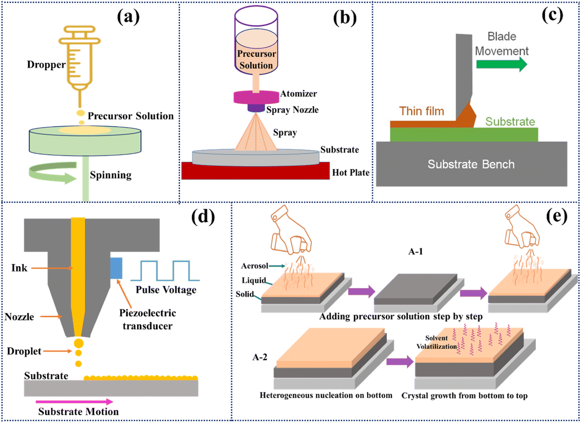
3.2.1. Spin coating process. The spin coating technique is one of the handy and extensively used techniques for fabricating thin films with controlled thickness and uniformity. According to this technique, the precursor solution is dropped onto the substrate, and then put on a spinning plate, which is rotated at a high angular velocity. As the solution spreads and the solvent evaporates, a uniform film is formed. The uniform and homogeneous thickness depends on the concentration of the solution, density and spinning rate of the rotor. In 2015, for the first time, Yakunin and colleagues fabricated a thin film of MAPbI3 by adopting four spin-cast layers with a thickness ranging from 260 nm to 600 nm using the spin-coating process, which was utilized in an X-ray detector. Later, different research groups developed different perovskite films for radiation detection such as organic, hybrid, and inorganic perovskite films.103–105 This process is depicted in Fig. 5(a).
 |
| | Fig. 5 Various methods for developing films: (a) spin coating; (b) spray coating; (c) doctor blade coating; (d) inkjet printing method; and (e) ALS technique. | |
3.2.2. Spray deposition process. The spray deposition technique is a cost-effective and large-scale perovskite film-developing methods. A spray coater is a specialized tool for uniform and controlled spray deposition. It is usually comprised of a nozzle or pump for solution distribution and a control system to move the substrate. In this process, the precursor solution is ejected from the nozzle as a droplet, and then this droplet particle hits the substrate. Over time, the droplets dry rapidly and form homogeneous films, the thickness of which can be adjusted by altering the deposition parameters including pressure, concentration, density and time.106 For the first time, the well-known research group led by S. Yakunin developed a thick MAPbI3 perovskite film (10–100 μm) for X-ray detection application by employing the spray deposition process.107 This technique is pictorially described in Fig. 5(b).
3.2.3. Aerosol-liquid–solid method (ALS). The ALS method is a smooth transition from aerosol to liquid, which has been used for the development of perovskite films. A suite of technical parameters including temperature, aerosol delivery rate and composition can be accurately controlled in the ALS method. The traditional solution-based methods including spin-coating faces a challenge in depositing a thick film on a substrate owing to limitations regarding the surface tension and viscosity. In contrast, the ALS method can successfully develop dense, highly crystalline perovskite films with low defects.108 For example, W. Qian and research team demonstrated the application of the ALS method to facilitate the growth of s uniform CsPbI2Br-based perovskite film for radiation detection and they showed that the thickness and grain size of the film were enhanced steadily with an increment in the growth time.109 Fig. 5(e) pictorially elucidates this process.
3.2.4. Dissolution and recrystallization method. The dissolution and subsequent recrystallization technique is an effective chemical process for developing crystal growth, compound purification and synthesis of materials with specific characteristics. In this technique, the sharp point or spike of the outer surface of the film is dissolved in the original perovskite solution after repeating the process. This dissolved material precipitates and fills the holes on the surface of the film at the appropriate temperature. After repetition of this process, a smooth and dense perovskite film is attained. For instance, in 2019, Z. Gou and colleagues obtained a high-quality film of microcrystalline CsPbBr3 after performing many repetition dissolutions and recrystallizations, providing a good route for attaining a high-performance X-ray detector.110 The SEM image of the film exhibited uneven surface with abundant gaps in the initial phase. However, with the repetition of the process, the CsPbBr3 film transformed into a smoother, microscopically porous structure. This conversion revealed that the sharp portion on the surface of the CsPbBr3 film gradually dissolved in the perovskite solution and filled the voids.
3.2.5. Inkjet printing method. Inkjet printing is a well-established and commonly used method for developing films. This process is advantageous from the aspect of low development costs and simple and flexible process. In addition, no mask plate or lithography is needed. This method involves the ejection of droplets of solution on the substrate from a chamber of solution by piezoelectric or thermal actuators. In 2019, the prominent research group of J. Liu and colleagues developed 20 nm-thick CsPbBr3 perovskite quantum dots for the first time by adopting the inkjet-printing method for the purpose of using them as an X-ray detector.111 Different research groups relied on this method to develop quantum dot-based films.112 It shows potential as an affordable and straightforward approach for the large-scale manufacturing of perovskite-based X-ray detectors with multi-channel arrays. This method is shown in Fig. 5(d).
3.2.6. Doctor blade method. The doctor-blade method is a very simple and facile technique where one blade is used as the tool. In general, it is adopted for the roll-to-roll printing process, where making mass customization is possible. In 2017, Y. C. Kim and research team synthesized an 830 μm-thick polycrystalline MAPbI3 film using a doctor blade as an initial example for the purpose of using it in radiation detection application.113 In 2023, J. Tan and research group manufactured a radiation detector based on the MAPbI3 perovskite with a thickness of 16.5 μm by adopting the doctor blade method.114 They also claimed that the sensitivity of the device was 127 μC Gy−1 cm− 2 under an irradiation dose rate of 0.1584 mGy s− 1 with good stability under ambient conditions for two months. This facile technique is depicted in Fig. 5(c).
3.2.7. Bar-assisted meniscus shearing method. A new and innovative approach named the bar-assisted meniscus shearing approach has been utilized to fabricate perovskite thin-films for application in radiation detection. This method involves the use of a solution of TIPS–pentacene and polystyrene to fabricate the detector. The research group led by I. Temiño showed that the coating speed and blend of bis(triisopropylsilylethynyl)pentacene:polystyrene are key tools to control the film morphology and carrier mobility, providing an enhancement in the detection capability of the device. They claimed that the recorded sensitivity of 1.3 × 10⁴ μC Gy−1 cm−2 and LDDR of 35 μGy s−1 were obtained for organic-based direct X-ray radiation detectors.115
3.3. Wafer
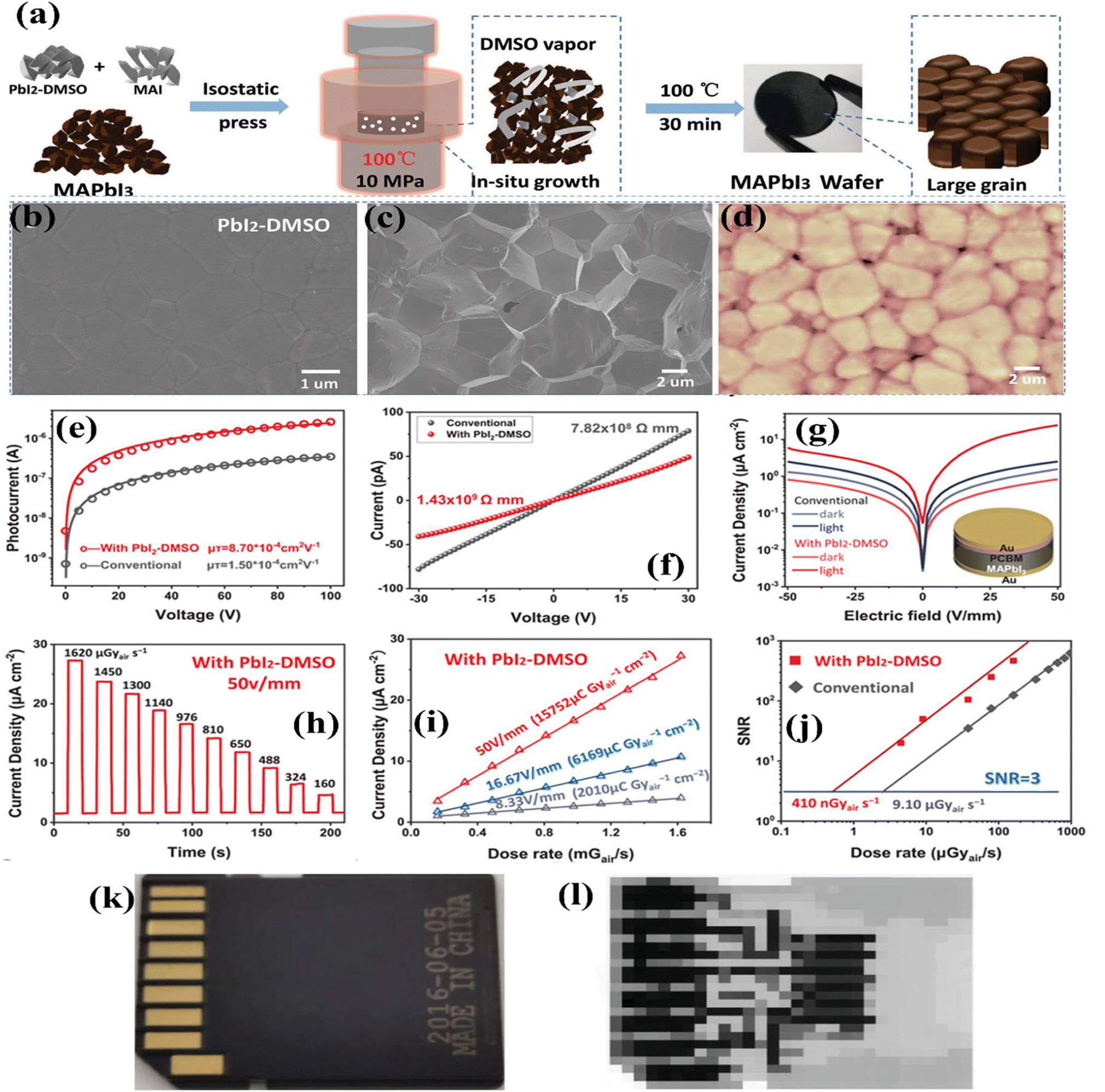
3.3.1. Isostatic-Pressing method. The development of large-area and millimeter-thick perovskite films for radiation sensing and imaging applications remains a major issue. The inevitable solvent evaporation during the solution-based method leaves a large number of pinholes inside the films, which significantly inhibit the charge transportation and reduce the performance of the device. Different research groups prepared perovskite-based wafers, which require no solvent throughout the process and result in a pinhole-free and compact wafers. The isostatic pressing scheme is a well-known method for preparing wafer-like structures. The isostatic pressing method provides an advantage in developing uniform and dense wafer structures, which can be useful in achieving high-quality perovskite wafers with better electrical and optical properties. According to this method, high-quality perovskite powder is prepared with an exact composition and particle size. Subsequently, the perovskite powder is placed in a flexible mold or container. Later, the mold containing the perovskite powder is exposed to high pressure uniformly from all directions by means of a fluid medium. This pressure causes the powder particles to compact and adhere together, forming a solid structure with the desired shape and dimension. After the pressing step, the developed wafer needs to go through additional treatments such as annealing to consolidate the structure and enhance its properties. The entire procedure of this technique is pictorially described in Fig. 6.
 |
| | Fig. 6 Isostatic-pressing method. | |
4. Perovskite material development and devices for X-ray detection
Recently, different researchers have devoted their efforts to applying OIH perovskites, all-inorganic halide perovskites and lead-free halide perovskites in radiation detection besides other applications including photovoltaic applications. Generally, the direct detection and scintillation mechanism are employed for the detection of high-energy radiation and imaging application. However, herein, we only focus on the direct detection of X-rays and imaging applications. There are notable reports on perovskite-based scintillators for high-energy radiation detection, high-resolution imaging, spectroscopy and timing applications.116–118 In addition, researchers have also paid attention to a new structure named anti-perovskite structure as a radiation detector. These materials are usually developed in the form of SCs, films and wafers for radiation detection. All these forms display distinct properties. For instance, SCs display lower defects and a lack of grain boundary. Consequently, this type of crystal possesses beneficial optoelectronic properties with respect to radiation detection. Alternatively, perovskite films are compatible with flexible substrates and large-area wafers can be developed without introducing a solvent.
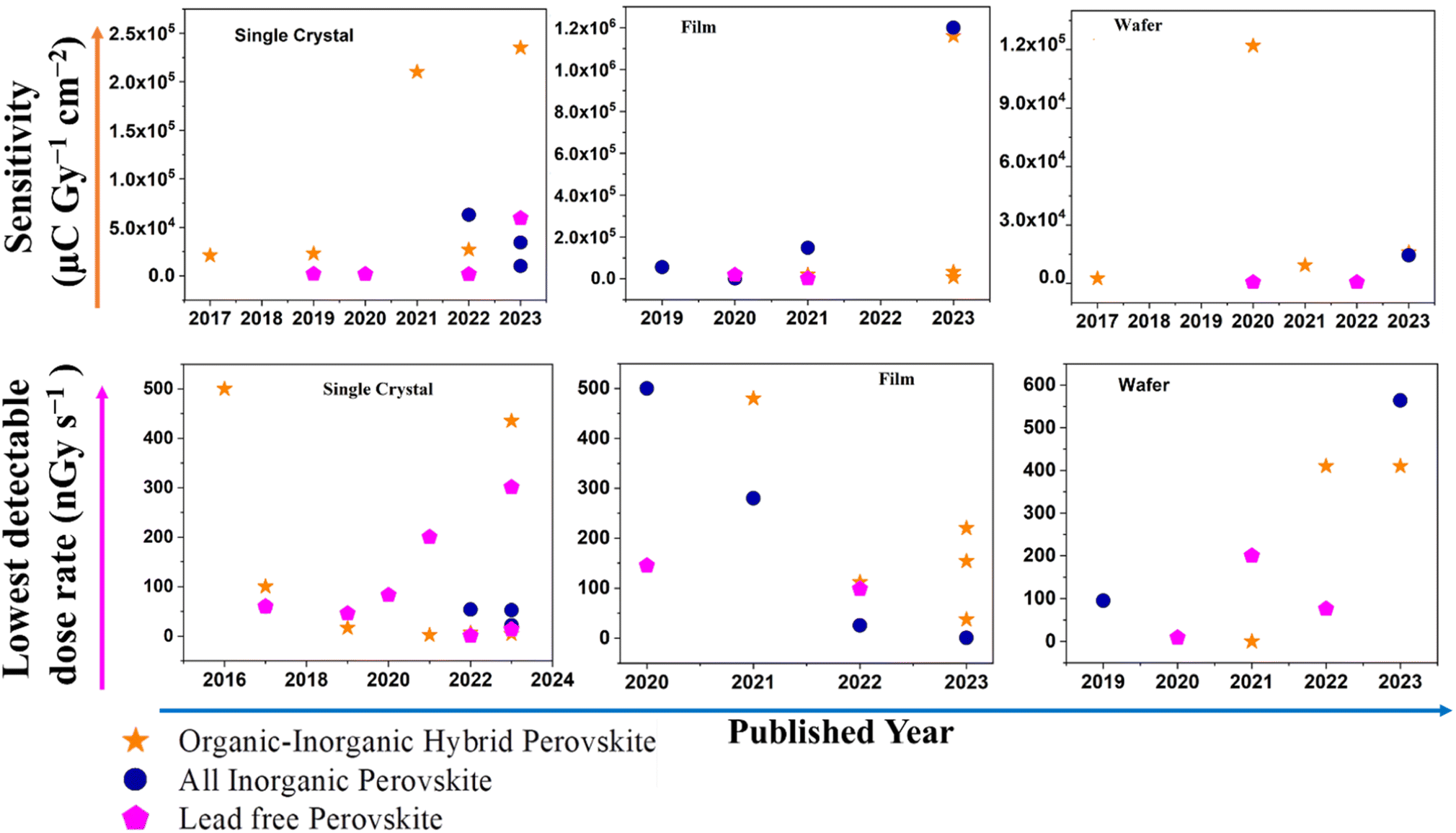
Therefore, in this section, we discuss some rewarding and meaningful research on perovskite-based radiation detection. Fig. 7 displays the sensitivity and LDDR of some representative works on SCs, films and wafers in OIH, all-inorganic and lead-free perovskite-based X-ray detectors. In addition, the performance of some conventional radiation detection devices is displayed in Table 1.
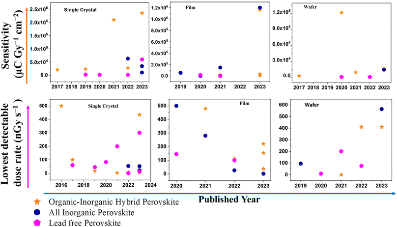 |
| | Fig. 7 Sensitivity and lower detection dose rate (LDDR) of SC-, film- and wafer-based hybrid, all-inorganic and lead-free perovskite-based detectors. | |
Table 1 Some representative works on conventional radiation detection devices
| Materials |
Device structures |
μτ product (cm2 V−1) |
Sensitivity (μC Gy−1 cm−2) |
LDDR (nGy s−1) |
Ref. |
| α-Se |
— |
3 × 10⁻⁷ to 10−5 |
20 |
5500 |
119 and 120 |
| Bi2O3 |
ITO/PEDOT:PSS/P3HT/PC70BM/Bi2O3/BCP/Al |
— |
1712 |
— |
121 |
| Bis-(triisopropylsilylethynyl) pentacene (TIPS) |
Au/TIPS/Au |
— |
77 |
— |
122 |
| TIPS |
Au/TIPS/Au |
— |
1.3 × 10⁴ |
35000 |
123 |
| InSe |
Ag/InSe/Ag |
∼7.12 × 10⁻⁴ |
3.96 |
6350 |
124 |
| CdTe |
— |
— |
318 |
50000 |
125–127 |
4.1. Organic–inorganic hybrid perovskite-based radiation detectors
Organic–inorganic hybrid perovskites display the highest efficiency in solar cell applications to date.128 They also exhibit promising optoelectronic characteristics for X-ray detection, featuring a high average atomic number, high bulk resistivity, substantial band gap ranging from 1.6 to 3.0 eV and high carrier mobility–lifetime product, typically around ∼10−2 cm2 V−1.129 Some meaningful and representative works are tabulated in Table 2.
Table 2 Organic–inorganic hybrid perovskite-based X-ray detectorsa
| |
Materials |
Methods |
Device structures |
μτ product (cm2 V−1) |
Resistivity (Ω cm) |
Sensitivity (μC Gy−1 cm−2) |
LDDR (nGy s−1) |
Spatial resolution (lp mm−1) |
Published year |
Ref. |
| Different layers (ETL, HTL, interfacial layer, electrodes) of the device are deposited onto developed perovskite layers by adopting commonly used techniques including thermal evaporation, sputtering method, spin coating, shadow mask technique, and high vacuum deposition. |
| Single crystal |
MAPbI3 |
Precipitation from a concentrated aqueous solution |
Connecting wire–MAPbI3–connecting wire |
— |
— |
75% of charge collection efficiency under 20–35 keV X-ray energy |
— |
— |
2015 |
130 |
| MAPbBr3 |
Anti-solvent method |
Au/MAPbBr3/C60/BCP/Ag |
1.2 × 10⁻² |
— |
80 |
500 |
— |
2016 |
39 |
| MAPbBr3 |
Low-temperature solution-based molecular bonding |
Au/BCP/C60/MAPbBr3/Si |
692 (lifetime) |
— |
2.1 × 10⁴ |
100 |
10 |
2017 |
131 |
| MAPbI3 |
ITC |
Au//Cr/MAPbI3/Cr/Au |
3.26 × 10⁻³ |
— |
968.9 |
— |
— |
2018 |
132 |
| GA0.16MA0.84PbI3 |
ITC |
Au/Perovskite/Ga |
7.2 × 10⁻³ |
— |
2.3 × 10⁴ |
16.9 |
— |
2019 |
133 |
| MAPbBr3 |
ITC |
Au/MoO3/MAPbBr3/Ag |
3.8 × 10⁻⁵ |
— |
2552 |
1200 |
— |
2020 |
134 |
| MAPbI3 |
ITC |
Cr/BCP/C60/oxysalt/MAPbI3/oxysalt/Cr |
1.3 × 10⁻² |
— |
2.1 × 10⁵ |
2.34 |
— |
2021 |
135 |
| Cs0.1FA0.85GA0.05Pb(I0.9Br0.1)3 doped with Sr2+ |
ITC |
Au/Cs0.1FA0.85GA0.05Pb(I0.9Br0.1)3 doped with Sr2+/Au |
1.29 × 10⁻² |
— |
2.7 × 10⁴ |
7.09 |
8.01 |
2022 |
136 |
| MAPbBr3 |
ITC |
Au/MAPbBr3/Au |
3.3 × 10⁻³ |
— |
2.35 × 10⁵ |
15.7 |
— |
2023 |
137 |
| (R)-(H2MPz)BiI5 (R-MPz = (R)-(−)-2-methylpiperazine) |
Low-temperature solution method |
— |
1.88 × 10⁻⁴ |
9.62 × 10¹⁰ |
263.58 |
435 |
— |
2023 |
138 |
| (1,5-PDA)BiI5 |
Liquid phase diffusion method |
Au/(1,5-PDA)BiI5/Au |
7.49 × 10⁻³ |
— |
8120 |
4.5 |
— |
2023 |
139 |
| Thin/thick film |
MAPbI3 |
Spray coating |
Ag/ZnO/PCBM/MAPbI3/PEDOT:PSS/ITO |
2 × 10⁻⁷ |
— |
25 |
— |
— |
2015 |
140 |
| MAPbI3 |
Spin coating |
ITO/PEDOT:PSS/MAPbI3/PCBM/Al |
— |
— |
12.5 A W−1 (responsivity) |
— |
— |
2016 |
141 |
| MAPbBr3–MAPbI3 |
Printed on thin-film transistor backplane |
ITO/PI-MAPbBr3/MPC/PI-MAPbI3/TFT backplane |
1 × 10⁻⁴ |
— |
11 |
— |
— |
2017 |
142 |
| Cs0.05FA0.79MA0.16Pb(I0.8 Br0.2)3 |
Anti-solvent technique |
FTO/c-TiO2/m-TiO2/perovskite/Spiro-OMeTAD/Au |
2.0 × 10⁻⁵ |
— |
97 |
— |
— |
2019 |
143 |
| MAPbI3−XClX |
Spin coating |
Ag/RhB101–LiF/PCBM/MAPbI3−XClX/PEDOT:PSS/ITO |
— |
— |
67 |
— |
— |
2020 |
144 |
| (PEA)2MA3Pb4I13 as 2D-MAPbI3 as 3D |
Sequential deposition method |
FTO/2D–3D/Carbon |
2.2 × 10⁻⁵ |
3 × 10⁹ |
1.95 × 10⁴ |
480 |
— |
2021 |
145 |
| BA2PbI4 as 2D-MAPbI3 as 3D |
MAPbI3 powder, pure BA2PbI4, and mixtures with a BA2PbI4 to MAPbI3 mass ratio of 1:19, 1:9, and 1:4 were loaded into the mold and further hot-pressed at 150 °C for 1 h to fabricate 3D and 2D materials |
Au/BA2PbI4–MAPbI3/Au |
1.18 × 10⁻³ |
4.34 × 10⁸ |
2.0 × 10³ |
111.76 |
— |
2022 |
146 |
| MA0.42FA0.58PbI3 |
Ultrasound-assisted crystallization with post hot-pressing technique |
Au/MA0.42FA0.58PbI3/FTO |
1.5 × 10⁻⁴ |
— |
1.16 × 10⁶ |
37.4 |
— |
2023 |
147 |
| MAPbI3 |
Ultrasonic spray coating process |
FTO/MAPbI3/C |
5.91 cm2 V−1 s−1 (mobility) |
— |
7304 |
154 |
— |
2023 |
148 |
| MAPbI3 |
Blade-coating method |
ITO/PEDOT:PSS/MAPbI3/PCBM/Au |
2.2 × 10⁻³ |
— |
3.26 × 10⁴ |
220 |
0.43 lp per pixel |
2023 |
149 |
| MAPbI3:Bi |
Spray coating technique |
ITO/n-MAPbI3/p-MAPbI3/Au |
— |
— |
1969.75 |
147 |
3.3 |
2023 |
150 |
| FA0.5MA0.5PbI3 |
Blade-coating method |
ITO/PEDOT:PSS/FA0.5MA0.5PbI3 microcrystalline films/fullerene (C60)/bathocuproine (BCP)/copper (Cu) |
1.1 × 10 −3 |
— |
6.1 × 10⁴ |
1.5 |
— |
2023 |
151 |
| Wafer |
CH3NH3PbI3 |
Ultrathin geometry-defined dynamic-flow reaction scheme |
Au/CH3NH3PbI3/Au |
39.6 cm2 V−1 s−1 (mobility) |
— |
— |
— |
— |
2016 |
152 |
| MAPbI3 |
Room-temperature sintering technique |
Glass/ITO/PEDOT:PSS/MAPbI3/PCBM/ZnO/Ag |
2 × 10⁻⁴ |
— |
2527 |
— |
— |
2017 |
153 |
| MAPbI3 |
The space-confined technique with seed-induced crystallization process |
Au/MAPbI3/Au |
— |
— |
Responsivity of 3.87 AW−1, and detectivity of 1.77 × 10¹³ Jones |
— |
— |
2019 |
154 |
| CH3NH3PbI3 |
One-step heat-assisted high-pressure press scheme |
Au/PCBM/CH3NH3PbI3/Au |
3.84 × 10⁻⁴ |
— |
1.22 × 10⁵ |
— |
— |
2020 |
155 |
| MAPbI3 |
The mechanical sintering of an independent absorber layer and the subsequent incorporation of this layer onto a pixelated backplane |
TFT backplane/pixelelectrode/pixel grid/MAPbI3/Cr |
4 × 10⁻⁴ |
— |
9300 |
0.22 |
6 |
2021 |
156 |
| MAPbI3–Cs3Cu2I5 |
— |
Au/Spiro-OMeTAD/MAPbI3/MAPbI3–Cs3Cu2I5/MAPbI3/C60/BCP/Cr |
— |
5.4 × 10⁷ (30% Cs3Cu2I5) |
885 (30% of Cs3Cu2I5) |
410 (30% of Cs3Cu2I5) |
— |
2022 |
157 |
| MAPbI3 |
Isostatic pressing method |
Au/PCBM/MAPbI3/Au |
8.70 × 10⁻⁴ |
1.43 × 10⁹ |
1.58 × 10⁴ |
410 |
— |
2023 |
158 |
4.1.1. Single crystal. The sensing ability of OIH perovskite SCs was reported by B. Náfrádi and team in 2015 although the first SC perovskite-based high energy radiation detector was developed in 2013 by the renowned research group of C. C. Stoumpos by adopting an all-inorganic perovskite material.130,159 The research group of Náfrádi developed OIH perovskite-based MAPbI3 SCs by adopting a temperature-lowering crystallization method, which were employed for detecting X-ray radiation directly.130 They used the perovskite SC material directly as a radiation detector without using any counter electrode. They observed that the stopping power of these SCs was superior to Si-based radiation detectors. Numerically, they showed that the 110 μm-thick MAPbI3 SC was needed to completely stop about 30 keV soft X-rays, where a one mm-thick Si-based detector is essential. In addition, this device showed a high CCE of 75% under the irradiation of 20–35 keV X-ray energy. They also investigated the device stability against X-rays and found that the photo-current decreased by less than 20% under a dose of 40 Sievert. Moreover, the humidity was responsible for the observed degradation rather than radiation because the device was not encapsulated. Finally, Monte Carlo simulations demonstrated the prospective of these SCs as radiation-shielding materials, where it was displayed that a 1 mm-thick MAPbI3 crystal can stop 2 MeV energy radiation. One year later, in 2016, H. Wei and colleagues fabricated MAPbBr3 perovskite-based SCs with a thickness of 2–3 mm for use as an X-ray radiation detector by utilizing the solution growth method named anti-solvent method.39 The device structure was Au/MAPbBr3/C60/BCP/Au. They claimed that they limited the bulk defects by optimizing the molar ratio of PbBr2/MABr as well as surface traps by UV-O3 treatment. Consequently, a high μτ product of 1.2 × 10⁻² cm2 V−1 and a small surface charge recombination velocity of 64 cm s−1 were observed. They also found that the LDDR was as low as 0.5 μGy s−1 together with a high sensitivity of 80 μC Gy−1 cm−2. This sensitivity was four-times larger than that achieved by using α-Se-based X-ray radiation detectors.119,120 Moreover, this device displayed 16.4% detection efficiency under continuous irradiation of X-ray energy of 50 keV without biasing. Another well-known research group, namely W. Wei et al., fabricated an Si-integrated MAPbBr3 OIH perovskite-based SC radiation detector by adopting the method of low-temperature solution-based molecular bonding with the help of brominated APTES molecules in 2017.131 They adopted the device structure of Au/BCP/C60/MAPbBr3/Si. In addition, they used a passivating layer together with an electrode to efficiently collect the charge carriers. This detector could detect an extremely low X-rays (8 keV) with a dose rate of less than 0.1 μGy s−1 together with high sensitivity of 2.1 × 10⁴ μC Gy−1 cm−2. This device showed 1000-times greater sensitivity than that of α-Se-based radiation detectors towards X-ray radiation. Furthermore, this device was capable of imaging with a (15–120)-fold weaker dose rate to the patient. Finally, they claimed that this detector was several degrees of magnitude better than the commercial α-Se-based X-ray radiation detectors because of these performances. In 2018, F. Ye et al. developed a high-energy radiation detector by adopting two shapes of MAPbI3 structures named d-MAPbI3 (nonrectangular dodecahedrons) and c-MAPbI3 (cuboid shaped) by means of the crystal growth technique ITC.132 The radiation detector structure was Au//Cr/MAPbI3/Cr/Au, where they used a 1 mm-thick perovskite layer for both shapes. According to the material characterization data, they observed a lower trap density in the c-MAPbI3 (1.14 × 109 cm−3) than that in the d-MAPbI3 (1.14 × 1010 cm−3) active layer, which was even six orders of magnitude lower than that of polycrystalline-based perovskite films.160,161 In addition, they also measured the carrier mobility, which was found to be 293 cm2 V−1 s−1 and 164 cm2 V−1 s−1 for c-MAPbI3 and d-MAPbI3, respectively. Moreover, the μτ product of c-MAPbI3 (3.26 × 10⁻³ cm2 V−1) was greater than that of the d-MAPbI3 (1.49 × 10⁻³ cm2 V−1) layer. Finally, the device with c-MAPbI3 showed better sensitivity under −1 V bias and irradiation of 50 keV high energy of X-rays. The sensitivity of the c-MAPbI3-based device was approximately 968.9 μC Gy−1 cm−2, whereas the d-MAPbI3-based device showed a sensitivity as low as 3.4 μC Gy−1 cm−2. Another group of Y. Huang and research team developed three perovskite-based high-energy X-ray radiation detectors by incorporating DMA+ (dimethylammonium) and GA+ (guanidinium) in the original MAPbI3 perovskite in 2019.133 These three actual active layers named MAPbI3, GA0.16MA0.84PbI3 and DMA0.14MA0.86PbI3 were developed by adopting the ITC growth technique. They used two structures named Au/perovskite/Au and Au/perovskite/Ga by adopting symmetric electrodes and asymmetric electrodes. Using asymmetric electrodes, they obtained a much lower Idark for GA0.16MA0.84PbI3 (4.5 nA cm−2) and DMA0.14MA0.86PbI3 (8.7 nA cm−2) than that of the original MAPbI3 (21.4 nA cm−2) SCs. In addition, they also reported that the μτ product (surface recombination velocity) of the GA0.16MA0.84PbI3, DMA0.14MA0.86PbI3 and MAPbI3 structures were 1.3 × 10⁻² cm2 V−1 (86 cm s−1), 7.2 × 10⁻³ cm2 V−1 (663 cm s−1) and 5.3 × 10⁻³ cm2 V−1 (1245 cm s−1), respectively. This indicates that the structure with GA0.16MA0.84PbI3 showed a better performance in terms of μτ and surface recombination velocity. Furthermore, the GA0.16MA0.84PbI3 and DMA0.14MA0.86PbI3 SCs showed a lower LDDR (16.9 nGy s−1) than that of pristine MAPbI3 (80.6 nGy s−1). Finally, the highest sensitivity was also displayed by the structure with GA0.16MA0.84PbI3 SC, which is about 2.3 × 10⁴ μC Gy−1 cm−2. Thus, by performing structural modification, one can achieve desirable structures for detecting X-ray radiation. In 2020, Z. Fan et al. fabricated a high-crystalline MAPbBr3 SC by employing the ITC method to detect ionizing radiation such as X-rays.134 For this purpose, they used two device structures of Au/MAPbBr3/Au and Au/MoO3/MAPbBr3/Ag, where the structure of Au/MoO3/MAPbBr3/Ag showed a better performance in X-ray radiation detection. They reported that the trap density and hole mobility for the MAPbBr3 SC were 2.26 × 109 cm−3 and 89.8 cm2 V−1 s−1, respectively. This larger carrier mobility and low trap density of the MAPbBr3 SC imply that MAPbBr3 is suitable for X-ray radiation detection. They also claimed a higher carrier lifetime and larger diffusion length, which were ∼422.85 ns and ∼10.66 μm, respectively. Finally, they reported the device sensitivity and the lowest detectable dose of radiation, which was observed to be 1.2 μGy s−1. In addition, the highest sensitivity of 2552 μC Gy−1 cm−2 was observed for the Au/MoO3/MAPbBr3/Ag structure. The authors mentioned in their article that due to the insertion of MoO3, the hole extraction increased, resulting in a better performance. The established research group led by Y. Liu fabricated a high-quality SC of MAPbI3 by adding 3-(decyldimethylammonio)-propane-sulfonate inner salt as a ligand with the help of the ITC crystal growth method in 2021.135 Due to the high crystallinity of the structure, the trap density was 7 × 1010 cm−3, which was 23-times smaller than that of the structure without additive.
They stated that the carrier mobility and μτ product were improved due to the addition of the OHIS additive material in the precursor solution of perovskite. The carrier mobility and μτ product improved from 72 cm2 V−1 s−1 to 112 cm2 V−1 s−1 and 8.4 × 10⁻³ cm2 V−1 to 1.3 × 10⁻² cm2 V−1, respectively. Finally, they tested the performance of this structure under X-rays of 8 keV and found the sensitivity of 2.1 × 10⁵ μC Gy−1 cm−2 with LDDR of 2.34 nGy s−1. In the medical sector, high energetic X-rays typically above 60 kVp are required due to their high penetration power. Therefore, X-rays having energy levels of 60 kVp, 100 kVp, and 120 kVp were used to simulate the energy spectrum of the 2.4 mm-thick crystal in this study. The detector exhibited the highest sensitivity of 2.9 × 10⁶ μC Gy−1 cm−2 with LDDR of 5.7 nGy s−1 for 60 kVp X-rays. In 2022, another research group of J. Jiang et al. synthesized three hybrid perovskite layers of MA-free named Cs0.1FA0.9Pb(I0.9Br0.1)3 (CsFA), Cs0.1FA0.85GA0.05Pb(I0.9Br0.1)3 (CsFAGA) and CsFAGA doped with Sr2+ (CsFAGA:Sr) by employing ITC SC growth method.136 Among them, the structure of CsFAGA:Sr showed a better performance for X-ray radiation detection. The incorporation of Sr2+ element modulated the optoelectronic features of the mother structures in favor of X-ray radiation detection. According to their report, the obtained charge mobility for the CsFA, CsFAGA and CsFAGA:Sr structures was 162 cm2 V−1 s−1, 241 cm2 V−1 s−1 and 288 cm2 V−1 s−1, respectively. A higher lifetime was also observed for the CsFAGA:Sr structure, which was 1059 ns. The μτ product and surface recombination velocity of the structure were also improved with respect to the other structures, which were 1.29 × 10⁻² cm2 V−1 and 82 cm s−1, respectively. In addition, promising sensitivity was also observed for the CsFAGA:Sr device under 1 V cm−1, which exhibited the highest sensitivity of 2.7 × 10⁴ μC Gy−1 cm−2, which was almost 33- and 2-times larger than that of the CsFA and CsFAGA structures at a dose rate of 155 nGy s−1, respectively. Moreover, they obtained a stable sensitivity of ∼2.6 × 10⁴ μC Gy−1 cm−2 for the CsFAGA:Sr structures under different dose rates (18–940 nGy s−1). However, the LDDR of 7.09 nGy s−1 was the lowest among the structures. In 2023, the prominent research group led by Q. Xu and colleagues fabricated an MAPbBr3 SC by utilizing a continuous solution growth technique to significantly decrease the formation of defects produced by the repetitive ITC technique.137 The device structure and dimensions were Au/MAPbBr3/Au and (40 × 40 × 2) mm3, respectively. They found a trap density as low as ∼8.22 × 108 cm−3 and high μτ product of 3.3 × 10⁻³ cm2 V−1. In addition, they also conducted studies on the sensitivity and LDDR. The highest X-ray sensitivity of 2.35 × 10⁵ μC Gy−1 cm−2 and LDDR of 15.7 nGy s−1 were recorded. They also performed a stability test by preserving the device in air with 60% humidity and 25 °C temperature. They had found that Idark increased significantly after 7 days. Alternatively, the device in an Ar-filled glove box displayed no change in Idark and photo-current after more than 100 days. Moreover, they developed a pixeled perovskite photoconductor system for imaging applications. The bottom and top electrodes of the device were constructed using a thin Au coating that was thermally evaporated. Then, they recorded the X-ray image of a hex nut with this direct-conversion pixelated device. The pulsed X-ray source (ULTRA 12040Hf Portable X-ray source) had a pulse length of 4 s and energy of 70 keV. The greatest photo-current to Idark ratio was 23.8 at a low dosage rate of 0.45 Gy s−1 and an applied electric field of 20 V mm−1. The X-ray image of the hex nut was developed by employing the photo-current to Idark ratio in each pixel. The spatial resolution was limited by the huge size of the pixels, resulting in a high-contrast picture. Thus, by optimizing the synthesis process, a highly efficient device could be attained. Fig. 8 depicts the crystallization technique, characterization, X-ray detection and imaging.
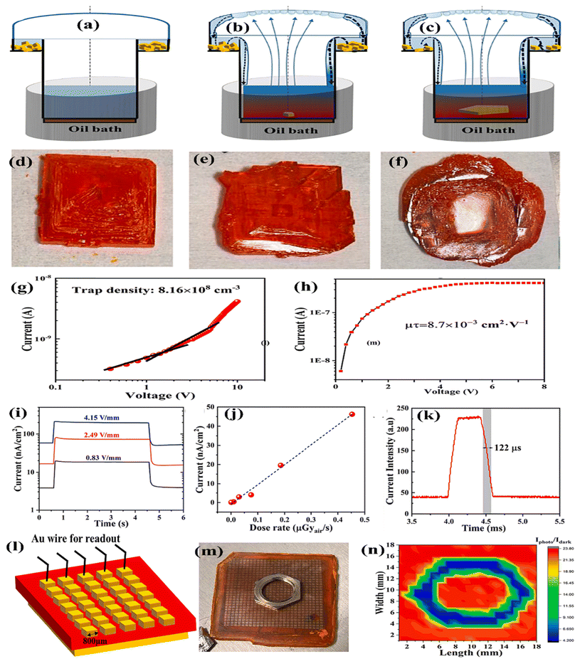 |
| | Fig. 8 (a–c) Continuous solution growth technique; (d–f) images of MAPbBr3 SCs; and (g) Idark curve for the device. (h) Current trace of the device across a bias range; (i) device current response to pulsed X-ray at various biases; (j) current response at various dose rates; (k) temporal photocurrent response for vertical surface detector; (l) schematic illustration of the imaging detector; (m) image of a hex nut on top of pixelated MAPbBr3 X-ray detector; and (n) X-ray image of the hex nut based on the ratio of photo-current (X-ray induced) to Idark. Reprinted with permission from ref. 137. Copyright 2023 Elsevier B.V. | |
4.1.2. Thin/thick film. Perovskite film developing processes are well-established compared to SC growth techniques in the case of solar cell fabrication. Recently, several research groups have been exploring the application of perovskite films in the field high-energy radiation detection. In 2015, for the first time, the research group of S. Yakunin developed a hybrid perovskite film with a large size (more than 250 nm) by adopting spray-coating solutions, where they used the common polar solvent DMF to dissolve MAPbI3.140 High crystallinity and large grain size are essential for efficient charge transportation. They observed a lower mobility–lifetime product of 2 × 10⁻⁷ cm2 V−1. Similarly, they also calculated the mobility and photoluminescence–lifetime, ranging from 4 × 10⁻⁷ cm2 V−1 to 1.3 × 10⁻⁶ cm2 V−1, which is much lower than that of SC-based radiation detectors. This reveals that high crystallinity and large grain size were not achieved for smooth charge transportation. They also investigated the sensitivity of the film under X-ray radiation. The observed sensitivity and responsivity were 25 μC mGy−1 cm−3 and 1.9 × 10⁴ carriers/photon under 37 keV X-ray energy, respectively. One year later, in 2016, C. Chen and research group fabricated a device using a hybrid perovskite film such as MAPbI3 by adopting the spin-coating technique.141 In this device, they used the common solar cell structure. Particularly, they utilized a hole transport and electron transport layer for efficiently collecting the charge carriers. The overall device structure was ITO/PEDOT:PSS/MAPbI3/PCBM/Al. They observed the behavior of the device upon exposure to X-ray irradiation and without X-ray irradiation. They found that the Idark of the device was as low as 2 nA, which was amplified up to 25 nA when the device was exposed to X-ray radiation. In addition, they claimed that the responsivity of their was 12.5 A W−1. Moreover, it has been established that although the performance especially the sensitivity of radiation detectors increases with the biasing voltage, it initiates background noise. In 2017, another well-known research group of Y. C. Kim fabricated a film for application in X-ray detectors by using polycrystalline MAPbI3, which was printed on a thin-film transistor backplane.142 They utilized a two-step solvothermal technique including α-terpineol to develop MAPbI3. Finally, they obtained a dense and viscous mixture, which was printed by employing the doctor blade method. The μτ product of the film was observed to be large with a value of 1 × 10⁻⁴ cm2 V−1. In addition, the sensitivity of the device was observed to vary from 1 to 11 μC mGy−1 cm−2 with a change in the electric field from 0.01 to 0.24 V μm−1. Two years later, in 2019, L. Basiricò and research team synthesized two X-ray radiation detectors with the help of adopting two hybrid perovskite materials including Cs0.05FA0.79MA0.16Pb(I0.8Br0.2)3 and MAPbI3 using the standard anti-solvent technique, where chlorobenzene was used as the anti-solvent.143 In this device architecture, a mesoporous electron transport layer together with a compact transport layer were utilized for elevating the interfacial band alignment with the perovskite material for efficient charge carrier collection. The structure of the device was FTO/c-TiO2/m-TiO2/perovskite/Spiro-OMeTAD/Au. They reported that the μτ product was double for the Cs0.05FA0.79MA0.16Pb(I0.8Br0.2)3 structure (∼2.0 × 10⁻⁵ cm2 V−1) compared to that of MAPbI3 (∼1.0 × 10⁻⁵ cm2 V−1). A similar pattern was also observed in the sensitivity of the structures. They claimed that they attained a self-powered radiation detector using this perovskite-based film. The sensitivity for the structure based on Cs0.05FA0.79MA0.16Pb(I0.8Br0.2)3 was of ∼3.7 μC Gy−1 cm−2 under no biasing. However, under a reverse bias of 0.4 V, the sensitivity of the structure increased to 97 μC Gy−1 cm−2 despite it being a film, which exceeds the values of sensitivity of the commercially available detectors such as poly-CZT and α-Se.119,120,124 In 2020, the research group of X. Liu et al. fabricated a hybrid perovskite-based X-ray radiation detector via the compositional engineering of MAPbI3−xClx through the spin-coating process.144 The structure of the detector was Ag/RhB101–LiF/PCBM/MAPbI3−xClx/PEDOT:PSS/ITO. They investigated the properties to justify the efficiency of device to detect high-energy radiation under 70 keV X-ray energy. They claimed that the sensitivity of their device was up to 67 μC Gy−1 cm−2, which is better than some traditional X-ray detectors. It was also revealed that an appropriate charge carrier transport layer and compositional engineering can help realize a relatively better radiation-detecting device. In addition, they also reported the lower detection ability of the device, which was about 0.2 mGy s−1. The established research group led by X. Xu fabricated an X-ray detection device by employing a 2D–3D double-layer perovskite film, where they utilized (PEA)2MA3Pb4I13 as the 2D layer and MAPbI3 as the 3D layer in the structure of FTO/2D–3D/carbon with help of the sequential deposition method in 2021.145 They claimed that the resistivity of the double-layer film increased from 3.5 × 10⁸ Ω cm to 3 × 10⁹ Ω cm due to the insertion of the 2D perovskite layer. They also reported the μτ product was 2.2 × 10⁻⁵ cm2 V−1. Consequently, this 2D–3D double-layered device displayed a high sensitivity of 1.95 × 10⁴ μC Gy−1 cm−2 as well as an LDDR of 480 nGy s−1. Thus, this is another strategy for the fabrication of efficient detectors by combining low-dimensional materials with 3D materials. In 2022, another research team consisting of Y. Xiao and colleagues synthesized a hybrid perovskite-based X-ray radiation detector by employing a 2D material embedded with a 3D material, where they utilized BA2PbI4 as the 2D material and MAPbI3 as the 3D material.146 The structure of the detector was Au/BA2PbI4–MAPbI3/Au. Their analysis reported that the ion migration and Idark were reduced significantly due to the presence of the 2D material in the structure and the obtained Idark drift was 4.84 × 10⁻⁵ nA cm−1 s−1 V−1. They also confirmed the performance of the device, where the X-ray sensitivity of this bulk 2D/3D heterostructure-based detector was 2.0 × 10³ μC Gy−1cm−2 and the lower detection limit was also as low as 111.76 nGy s−1 under biasing of 10 V. In 2023, the prominent research group of W. G. Li et al. fabricated a device based on an MA0.42FA0.58PbI3 film with the help of ultrasound-assisted crystallization with post hot-pressing technique.147 This film growth technique offers homogeneous nucleation, large grain size, less defects, and quasi-monocrystalline film. After the post-hot-pressing curing, the carrier mobility and μτ product improved from 1.8 cm2 s−1 V−1 to 23.5 cm2 s−1 V−1 and from 8.4 × 10⁻⁶ cm2 V−1 to 1.5 × 10⁻⁴ cm2 V−1, respectively. Accordingly, an efficient MA0.42FA0.58PbI3 quasi-monocrystalline-based X-ray detection device was accomplished with remarkably high sensitivity of 1.16 × 10⁶ μC Gy−1 cm−2 and LDDR of 37.4 nGy s−1. In 2023, another eminent researcher J. Zhao and colleagues synthesized an X-ray-detecting device, which was also employed to image an object.150 They achieved a successful device by fabricating an MAPbI3 active film utilizing the spray-coating method. They adopted a strategy to make a more efficient layer by incorporating Bi3+. They claimed that their 5% Bi3+-doped layer lowered the Idark by
an order of magnitude compared to the pristine film. The device structure was ITO/n-MAPbI3/p-MAPbI3/Au, where pristine MAPbI3 displayed weak p-type characteristics, and n-MAPbI3 indicated 5% Bi3+ doping in MAPbI3. The device was confirmed to exhibit a high sensitivity of 1969.75 μC Gy−1 cm−2 and LDDR of 147 nGy s−1. In addition, the device exhibited outstanding flexibility and durability, where it sustained a high performance after being bent 2000 times or kept at 30–50% RH under environmental conditions for more than a month. For the imaging, they fabricated a flexible X-ray detector with a size of 100 cm2 and verified the homogeneity of the device by measuring the dark and X-ray illumination response currents of a chosen 5 × 5 pixel array. Each pixel was 4 mm2 in size and 1 mm at a distance. The dark and X-ray illumination response currents were estimated to be 267–294 nA and 470–510 nA, respectively. The spatial resolution of the device was about 3.3 lp mm−1 in the flat state and 3.1 lp mm−1 in the bent state. The X-ray images of the letters SEU were recorded in the flat state and bent state, where the letters were clearer for the bent detector than the flat detector. They also took another image of a piece of ham with a nail inside to simulate human body injury, where the hole and nail inside the ham were observed in the X-ray image. Ultimately, they demonstrated the potential of the device in X-ray detection and imaging applications. The entire procedure of film development, characterization, X-ray detection and imaging is depicted in Fig. 9.
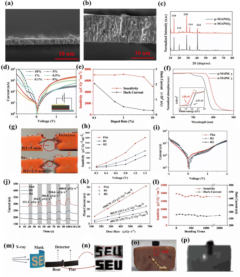 |
| | Fig. 9 (a) Cross-sectional SEM images of the Bi-doped MAPbI3 film; (b) cross-sectional SEM images of the p–n junction; (c) XRD outlining of the original p-MAPbI3 layer, and Bi-doped n-MAPbI3 layer; (d) dark I–V curves of the device with different Bi3+ concentrations; (e) X-ray (40 kV) sensitivity and Idark with respect to different Bi3+ concentrations at a biasing voltage 1 V; (f) absorption spectra of the n-MAPbI3 and p-MAPbI3 layers and curves of (αhν)2 versus photon energy (inset); (g) snapshot of the bent X-ray detector (the bending radius is indicated by the red line in the circle); (h) sensitivity versus biasing voltage under illumination with a 40 kV X-ray source; (i) I–V curves attained under different bending radii; (j) I–T curves and (k) photo-current versus dose rate at 1 V under altering bending radii with respect to different dose rates; (l) sensitivity of the device under flat circumstances after 2000 bends with a 5 mm bending radius; (m) experimental X-ray imaging setup (schematic) during planar and curve X-ray imaging; (n) planar in top and curved in bottom X-ray imaging showing the “SEU” symbol; (o) real object of a ham with a nail and (p) X-ray images of a piece of ham with a nail inside. Reprinted with permission from ref. 150. Copyright 2023 @ The Royal Society of Chemistry. | |
4.1.3. Wafers. Perovskite materials in the form of wafers offer a favorable and simplistic route for scaled-up applications including large and wearable flat panels, making them superior to other types of perovskite-based radiation detectors.162 A perovskite wafer, when fabricated without the introduction of a solution, realizes almost 100% utilization of materials because it directly transforms the initial precursor materials into the desired perovskite structure. In this section, we focus on the optoelectronic properties and performance of wafers for radiation detection. In 2016, Y. Liu and research team developed a wafer of MAPbI3 for radiation detection by employing an ultrathin geometry-defined dynamic-flow reaction scheme.152 The structure of the device was Au/MAPbI3/Au. After the fabrication of the device, they basically investigated the optoelectronic properties for radiation detection. They reported a low trap density of 6 × 108 cm−3, which is extremely low in comparison with the previously reported data, and the carrier mobility was 39.6 cm2 V−1 s−1. Their radiation detector was more responsive towards radiation than that of a microcrystal thin film.152 Particularly, they observed 350-times greater responsivity for the MAPbI3 SC wafer than a thin film under irradiation of 100 mW cm−2 with biasing of 2 V. As part of another initiative in 2017, the research group of S. Shrestha created a series of wafers by using the hybrid perovskite material MAPbI3 adopting a room-temperature sintering technique.153 The size of the wafer was half-inch in diameter and 200 μm to 1 mm in thickness. In addition, the density of the wafer was 3.76 g cm−3, which is close to the density of the MAPbI3 SC (4.15 g cm−3).163,164 Moreover, they have reported the ambipolar μτ product with a value of 2 × 10⁻⁴ cm2 V−1. Consequently, they found the excellent sensitivity of 2527 μC Gy−1 cm−2 under 70 kVp X-ray irradiation with a 0.2 V μm−1 electric field. Two years later, in 2019, J. Gao and colleagues fabricated a wafer-based radiation detector with the help of MAPbI3 by utilizing the combination of the space-confined technique with seed-induced crystallization process.154 Their developed wafers were as large as 10 mm without grain boundaries. The structure of the device was Au/MAPbI3/Au. This radiation detector with outstanding crystal quality demonstrated remarkable performance features. They also claimed that they achieved a lower trap density of 2.36 × 1010 cm−3, which was lower than that of polycrystalline thin films. In addition, the device displayed a light on/off current ratio of 4.3 × 10³, response time of 770 μs, and linear dynamic range of 119 decibels. Moreover, even at very low irradiation levels of 80 nW cm−2, this device demonstrated an exceptional external quantum efficiency of 904%, responsivity of 3.87 A W−1, and detectivity of 1.77 × 10¹³ Jones. Furthermore, they also investigated the stability issue and found more than 80% of the initial photo-current was maintained after 30 days of air storage. The research group comprised of M. Hu and colleagues fabricated an X-ray radiation detection device with the help of an MAPbI3 wafer in 2020.155 They utilized a one-step heat-assisted high-pressure pressing scheme, which enabled the fabrication of large-size wafers. The carrier mobility of the attained wafer was ∼20 cm2 V−1 s−1. Accordingly, the μτ product was as high as 3.84 × 10⁻⁴ cm2 V−1. For the purpose of performance evaluation, the adopted structure of their device was Au/PCBM/MAPbI3/Au. When subjected to an X-ray source with an acceleration voltage of 40 kV, the detector displayed an outstanding X-ray sensitivity as high as 1.22 × 10⁵ μC Gy−1 cm−2 under a biasing voltage of 10 V. This approach provides a convenient technique for developing sizable perovskite wafers with favorable optoelectronic properties for radiation detection. In 2021, S. Deumel and team adopted a two-step fabricating system for the formation of an X-ray flat-panel detector by employing MAPbI3 based on the mechanical sintering of an independent absorber layer and the subsequent incorporation of this layer onto a pixelated backplane.156 The wafer, which was made of freestanding microcrystalline MAPbI3, demonstrated sensitivity of 9300 μC Gy−1 cm−2 together with a μτ product of 4 × 10⁻⁴ cm2 V−1. The resulting X-ray imaging device, featuring 508 pixels per inch, attained an inspiring combination of high spatial resolution at six line pairs per millimeter and an LDDR of 0.22 nGy S−1 per frame. In 2022, the prominent research group of L. Liu et al. developed a device for X-ray detection by adopting a novel direct-indirect hybrid perovskite wafer with the help of a fast-tableting process.157 The device structure was Au/Spiro–OMeTAD/MAPbI3/MAPbI3–Cs3Cu2I5/MAPbI3/C60/BCP/Cr. Because of the fast energy transfer from Cs3Cu2I5 to MAPbI3, the device response time towards X-rays was significantly reduced by almost 30-fold, resulting in a rapid detection capability for a large-area detector array in under 1 s. In addition, the reported resistivity value of the 30% Cs3Cu2I5 wafer was 5.4 × 10⁷ Ω cm, which was 1.21-times higher than that of the MAPbI3 wafer. They also revealed that the sensitivity of the device regularly decreased with an increase in the content of Cs3Cu2I5. The device with 30% of Cs3Cu2I5 had the lowest detection dose rate of 0.41 μGy s−1, which was much lower than the real dose rate of 5.5 μGy s−1 throughout CT imaging. In addition, this value was also 1.5-times and 10-times lower than that of the direct-type MAPbI3 semiconductor and the Cs3Cu2I5 scintillator, respectively.165 Finally, the sensitivity of this hybrid X-ray detector was enhanced by 28 times in comparison with the indirect-type scintillator. Very recently, in 2023, the well-established research group led by W. Liu prepared a high-crystalline MAPbI3-based perovskite wafer with the help of PbI2–DMSO powder as an additive for X-ray detection.158 The white PbI2–DMSO powders were obtained by annealing a complex solution PbI2–DMSO, where DMSO was vaporized during annealing. During the process of isostatic pressing, a mixture of PbI2–DMSO, MAI, and MAPbI3 was combined and compressed on the perovskite wafer. At a relatively lower annealing temperature, the release of DMSO as vapor from PbI2–DMSO led to the spontaneous growth of crystals within the perovskite wafer. This provided a route for increasing the grain size, together with the passivation of grain boundaries as well as reducing the defect densities. Consequently, a dense and compact MAPbI3 wafer was obtained with a lower trap density of 1.22 × 1010 cm−3 and greater carrier mobility of 3.5 cm2 V−1 s−1 with respect to the traditional device (1.63 × 1010 cm−3 and 1.3 cm2 V−1 s−1, respectively).158 In addition, the device displayed a high μτ product with a value of 8.70 × 10⁻⁴ cm2 V−1. Moreover, they claimed that the higher sensitivity and LDDR were 1.58 × 10⁴ μC Gy−1 cm−2 and 410 nGy s−1, respectively. They also performed the imaging test of the device by taking an image of a memory card consisting of a plastic case and metal core. They successfully obtained a clear image of the memory card using this device. Thus, this study demonstrated an efficient strategy for perovskite wafer-based devices for X-ray radiation detection and imaging. The wafer development, characterization, X-ray detection and imaging are depicted in Fig. 10.
 |
| | Fig. 10 (a) Schematic illustration of preparation of PbI2–DMSO-assisted isostatic pressing of MAPbI3 wafer; (b) SEM images (top view); (c) SEM images (cross-sectional); (d) AFM images; (e) photoconductivity; (f) resistivity; (g) J–V characteristics; (h and i) PbI2–DMSO-assisted MAPbI3 device: current densities versus function of dose rate at different electric fields; (j) dose rate dependent SNR of the device; (k) photograph of a memory card and (l) X-ray image of the memory card. Reprinted with permission from ref. 158. Copyright 2023 @ Wiley Online Library. | |
4.2. All-inorganic halide perovskite detectors
Although X-ray radiation detectors based on OIH perovskites have exhibited a noteworthy performance, the stability of these hybrid materials is lacking. Specifically, their extreme sensitivity towards light, heat, oxygen and moisture are the reasons for this low stability.166 All-inorganic perovskites are expected to be the future X-ray detecting materials owing to their comparatively better stability than hybrid perovskites. Some representative works are presented in Table 3.
Table 3 All-inorganic perovskite-based X-ray detectorsa
| |
Materials |
Methods |
Device structures |
μτ product (cm2 V−1) |
Resistivity (Ω cm) |
Sensitivity (μC Gy−1cm−2) |
LDDR (nGy s−1) |
Spatial resolution (lp mm−1) |
Published year |
Ref. |
| Various layers (ETL, HTL, interfacial layer, electrodes) applied to pre-existing perovskite layers using standard techniques such as thermal evaporation, sputtering, spin coating, shadow mask application, and high vacuum deposition. |
| Single crystal |
CsPbBr3 |
Vertical Bridgman technique |
— |
1.7 × 10⁻³ |
3.43 × 10¹¹ |
Distinguished the Kα and Kβ peaks |
— |
— |
2013 |
167 |
| Cs2AgBiBr6 |
ITC |
Au/Cs2AgBiBr6/Au |
6.3 × 10⁻³ |
1.60 × 10¹¹ |
105 |
59.7 |
— |
2017 |
168 |
| Cs2AgBiBr6 |
ITC |
Au/Cs2AgBiBr6/Au |
— |
3.6 × 10¹² |
988 |
|
— |
2018 |
169 |
| PEA–Cs2AgBiBr6 |
Solution-processed uniformly cooling method |
Au/PEA–Cs2AgBiBr6/Au |
1.94 × 10⁻³ |
— |
288.8 |
— |
— |
2019 |
170 |
| CsPbBr3 |
Anti-solvent crystallization process |
Au/CsPbBr3/MoO3/Au |
6.69 × 10⁻⁸ |
— |
619 |
20900 |
— |
2020 |
171 |
| CsPbBr3 |
ITC |
ITO/NiOx/poly-TPD/CsPbBr3 SCs/C70/BCP/Cu |
160 cm2 V−1 s−1 (electron mobility) |
— |
4086 |
— |
— |
2021 |
172 |
| CsPbBr3−nIn |
Bridgman method |
Au/CsPbBr3−nIn/Au |
— |
2.2 × 10¹¹ (CsPbBr2I) |
6.3 × 10⁴ (CsPbBr2.9I0.1) |
54 (CsPbBr2I) |
— |
2022 |
173 |
| CsPbBr3 |
Vertical Bridgman furnace |
EGaIn/CsPbBr3/Au |
5 × 10⁻³ |
— |
34449 |
52.6 |
— |
2023 |
174 |
| CsPbBr3 |
Bridgman growth |
GaIn/CsPbBr3/Au |
1.34 × 10⁻³ |
— |
∼10283 |
22 |
— |
2023 |
175 |
| Thin/thick film |
Cs2TeI6 |
E-spraying procedure |
FTO/c-&m-TiO2 + Cs2TeI6/PTAA/Au |
5.2 × 10⁻⁵ |
4.2 × 10¹⁰ |
19.2 |
|
— |
2018 |
176 |
| CsPbBr3 |
Hot-pressing method |
FTO/CsPbBr3/Au |
1.32 × 10⁻² |
— |
55684 |
— |
— |
2019 |
177 |
| CsPbBr3 |
Scalable melt process |
Ga/CsPbBr3/FTO |
— |
8.5 × 10⁹ |
1450 |
500 |
— |
2020 |
178 |
| CsPbI2Br |
Aerosol-liquid–solid approach |
Carbon/perovskite/FTO |
1.14 cm2 V−1 s−1 (mobility) |
— |
1.48 × 10⁵ |
280 |
— |
2021 |
179 |
| CsPbI2Br |
Vacuum-deposited technique |
ITO/Ca/C60/CsPbI2Br/TAPC/TAPC:MoO3/MoO3/Ag |
18.804 cm2 V−1 s−1 (hole mobility) |
— |
1.2 × 10⁶ |
25.69 |
— |
2022 |
180 |
| CsPbBr3:Sr |
Anti-solvent method |
Au/PCBM/CsPbBr3:Sr/PEDOT:PSS/ITO |
— |
— |
517.02 |
0.955 |
— |
2023 |
181 |
| CsPbBr3 |
Electrospraying procedure |
Au/CsPbBr3/PI |
— |
1.14 × 10⁹ |
823.12 |
14.61 |
— |
2023 |
182 |
| Wafer |
CsPbBr3 |
Hot isostatic pressing technique |
Au/PCBM/CsPbBr3/Au |
5.16 × 10⁻⁴ |
3.16 × 10⁸ |
14430 |
564 |
— |
2023 |
183 |
| CsPbBr3–CsPb2Br5–CsPbIxBr3−x composite |
Water-assisted co-precipitation and spray coating |
Ag/wafer/Ag |
1.01 × 10⁻³ |
1.3 × 10⁹ |
20555.1 |
127.7 |
— |
2023 |
184 |
4.2.1. Single crystals. In 2013, the well-known research group of C. C. Stoumpos and colleagues developed an SC ingot of CsPbBr3 with a diameter of 7 mm and thickness of 2.1 mm by adopting the vertical Bridgman technique for radiation detection.167 They reported that their structure possessed a high carrier mobility and μτ product, which were detected to be 1000 cm2 V−1 s−1 and 1.7 × 10⁻³ cm2 V−1, respectively. In addition, they also reported that their structure attained a resistivity as high as 3.43 × 10¹¹ Ω cm, which is essential to inhibit Idark. Actually, these properties are essential for X-ray radiation sensing and imaging. They also investigated the suitability of the material as a detector by utilizing Ag as the X-ray source with the energy of 21.59 keV. The structure could distinguish the Kα and Kβ peaks. However, the sensitivity of the response was approximately 1% of that of the standard CZT detector. After a few years, in 2017, the research group of W. Pan fabricated a high-crystalline Cs2AgBiBr6 SC by employing the popular ITC method for the detection of X-rays.168 They made a symmetric device utilizing the structure of Au/Cs2AgBiBr6/Au. They extensively investigated and compared the carrier transportation properties with other reported studies. They observed the trap density as low as 1.74 × 109 cm−3 and carrier mobility as high as 11.81 cm2 V−1 s−1. Subsequently, the μτ was observed to be 6.3 × 10⁻³ cm2 V−1, which is comparable to that of MAPbBr3 (1.4 × 10⁻² cm2 V−1), MAPbI3 (1.0 × 10⁻² cm2 V−1) and the best-quality CdZnTe SCs (9.1 × 10⁻³ cm2 V−1). They also reported the highest resistivity of 1.60 × 10¹¹ Ω cm. This higher resistivity is the reason for the lower background current, and accordingly lower noise current. They evaluated the performance of the device under a tungsten anode X-ray tube with X-ray photon energy of up to 50 keV and peak intensity at 30 keV. The device displayed a good sensitivity of 105 μC Gy−1 cm−2 and LDDR of 59.7 nGy s−1. In 2018, as another initiative, the research team of J. A. Steele and colleagues synthesized a device with the structure of Au/Cs2AgBiBr6/Au for radiation detection under different temperature conditions.169 They observed a poorer performance at room temperature than that at liquid-N2 temperature due to the poor charge carrier dynamics. After reducing the temperature from room temperature to liquid-nitrogen for the Cs2AgBiBr6 structure, they observed a substantial improvement in the charge carrier life time from 700 ns to 1500 ns, which indicates the huge reduction in the negative impact of both parasitic recombination paths and Idark. Subsequently, the sensitivity of the device was enhanced from 316 μC Gy−1 cm−2 at room temperature to 988 μC Gy−1 cm−2 at liquid-N2 temperature. One year later, in 2019, W. Yuan et al. prepared two devices for X-ray radiation detection utilizing pristine Cs2AgBiBr6 and PEA–Cs2AgBiBr6 SCs with the structure of Au/perovskite/Au.170 They reported the trap density of 6.04 × 109 cm−3 and 3.43 × 109 cm−3 for the structure of Cs2AgBiBr6 and PEA–Cs2AgBiBr6, respectively. In addition, the observed carrier mobility of the pristine Cs2AgBiBr6 and PEA–Cs2AgBiBr6 SCs was 2.25 cm2 V−1 s−1 and 55.7 cm2 V−1 s−1, respectively. Moreover, the μτ product of Cs2AgBiBr6 and PEA–Cs2AgBiBr6 was observed to be 9.14 × 10⁻⁴ cm2 V−1 and 1.94 × 10⁻³ cm2 V−1, respectively. According to these results, the best sensitivity of these two devices was found to be 165.6 μC Gy−1 cm−2 and 288.8 μC Gy−1 cm−2 under a field of 22.7 V mm−1, respectively. Another research group led by Z. Fan synthesized two radiation detection devices by adopting CsPbBr3 SCs without and with an MoO3 HTL by means of the anti-solvent crystallization process in 2020.171 The structures were Au/perovskite/Au and Au/perovskite/MoO3/Au. The trap density and mobility of the carrier were observed to be 3.87 × 1010 cm3 and 10.7 cm2 V−1 s−1, respectively. In addition, the average lifetime of the carrier was (6.25 ± 1.06) ns. Moreover, they investigated the sensitivity of these two structures under a 50 kV tungsten anode X-ray tube. They observed the highest sensitivity in the case of the structure of Au/perovskite/MoO3/Au compared to that of Au/perovskite/Au. Particularly, the observed values for the structures with MoO3 and without MoO3 were 619 μC Gy−1 cm−2 and 200 μC Gy−1 cm−2 under an electric field of 45 V cm−1, respectively. Basically, this can be attributed to the increase in hole carrier collection by the HTL. In 2021, J. Peng et al. fabricated two devices for X-ray detection with CsPbBr3 SC developed in DMSO and CsPbBr3 SC developed in water.172 The SC grown in DMSO was fabricated by adopting modified ITC, while an SC was grown in water by gradually reducing the temperature of the water solution. The device structures were ITO/NiOx/poly-TPD/perovskite/C70/BCP/Cu. Here, they employed a charge carrier transporting and passivating layer for making the band alignment with the perovskite layer convenient. They observed a better performance in the case of the structure developed in water. Specifically, the mobility for holes and electrons in CsPbBr3 developed in water was 128 cm2 V−1 s−1 and 160 cm2 V−1 s−1, whereas it was 12.8 cm2 V−1 s−1 and 28.5 cm2 V−1 s−1 for CsPbBr3 synthesized in DMSO, respectively. The devices performance was estimated under the spectrum of X-rays from a tungsten anode tube functioning at 60 kVp. They claimed that the device grown in water displayed a high sensitivity of 4086 μC Gy−1 cm−2 towards X-rays, which is almost 200-times superior to that of commercial α-Se detectors (20 μC Gy−1 cm−2).172 In 2022, the prominent research group consisting of P. Zhang and colleagues fabricated a device with a CsPbBr3−nIn SC by incorporating iodine into pristine CsPbBr3.173 The structure of the device was Au/CsPbBr3−nIn/Au. They reported a higher resistivity for the structure with iodine in comparison with the pristine structure, with values of 3.6 × 10⁹ Ω cm (pristine CsPbBr3) and 2.2 × 10¹¹ Ω cm (CsPbBr2I). They also performed a sensitivity test under 120 keV hard X-rays with an electric field of 5000 V cm−1. The champion sensitivity of 6.3 × 10⁴ μC Gy−1 cm−2 was observed for the device with the CsPbBr2.9I0.1 SC and an LDDR of 54 nGy s−1 was obtained for the detector with CsPbBr2I SC. Thus, the incorporation of foreign atoms or doping strategy can be adopted to enhance the optoelectronic features of the devices. Recently, in 2023, the established research team led by Y. Hua fabricated a radiation detector with a CsPbBr3 SC by utilizing a homemade dual-temperature zone vertical Bridgman furnace.174 The temperature of the upper zone and lower zone of the furnace was approximately 640 °C and 300 °C, respectively. The structure of the device was GaIn/CsPbBr3/Au. They investigated the performance of the device and found anisotropic behavior along the [100], [010], and [001] orientations of the bulk CsPbBr3 SC. Among the orientations, the (010) surface of the structure displayed a better performance in terms of reducing defects and enhancing the carrier transportation due to the specific arrangement
of positive and negative charge distribution and the connection between the [PbBr6]4− octahedrons. Furthermore, the (010)-oriented crystal exhibited the lowest ion migration owing to its high active energy (143.77 meV) and ion diffusion barrier (0.361 eV), making it a favorable choice for improving the X-ray response. The device with the (010) orientation demonstrated the champion sensitivity of 34449 μC Gy−1 cm−2 under a biasing of −400 V and the LDDR of 52.6 nGy s−1 in comparison with the other two orientations. The entire procedure of the crystal development technique, characterization, and X-ray detection is depicted in Fig. 11.
 |
| | Fig. 11 (a) Schematic diagram of the vertical Bridgman furnace. (b) Photograph of an as-grown CsPbBr3 SCs. (c) XRD patterns of the (100), (010), and (001) facets of processed and polished wafers. (d–f) Photo-current fitting curves of the [100], [010], and [001] facets, respectively. (g) Photo-current response versus dose rates at −400 V. (h and i) X-ray sensitivities of the (100), (010), and (001) facet devices under various voltages. (j) Comparison of Idark drifts for the (100), (010), and (001) facet devices under a biasing voltage of −10 V. (k–m) Responses and SNR values dependent on the dose rate from 135 nGy s−1 to 260 nGy s−1 for the (100), (010), and (001) facet devices, respectively. (n) Detection limits (derived from the fitting line with an SNR of 3). Reprinted with permission from ref. 174. Copyright 2023@ The Royal Society of Chemistry. | |
4.2.2. Thin/thick films. In 2018, the eminent research group led by Y. Xu fabricated a device for the direct conversion of X-ray photons to current by utilizing an all-inorganic perovskite film.176 The film was developed with the help of a one-step coating technique (E-spraying procedure). The device structure was FTO/c-&m-TiO2 + Cs2TeI6/PTAA/Au. Their extensive investigation revealed that the film resistivity was 4.2 × 10¹⁰ Ω cm and the electron drift-length was 200 μm under 400 V cm−1. In addition, the μτ product for electrons was assessed to be 5.2 × 10⁻⁵ cm2 V−1. Furthermore, the sensitivity test of the device was accomplished under the irradiation from an Ag X-ray cathode with photon energy of 40 kVp. The sensitivity of 19.2 μC Gy−1 cm−2 was observed under an electric field of 250 V cm−1. Another research group of W. Pan et al. fabricated an inorganic perovskite CsPbBr3 film via the hot-pressing method for the detection of X-ray photons.177 The structure of the detector was FTO/perovskite/Au. The carrier mobility for the film of a gradually cooled perovskite film was greater (average 70 cm2 V−1 s−1) than that of the faster cooled perovskite film (12.3 cm2 V−1 s−1). Consequently, the μτ was better (1.32 × 10⁻² cm2 V−1) for the slowly cooled perovskite film than the faster cooled perovskite film (5.12 × 10⁻³ cm2 V−1). This was attributed to the formation of less defects during the slow cooling process. For the evaluation of the device performance, it was exposed to a tungsten anode X-ray source with a photon energy of 50 keV. The champion performance was recorded to be 55684 μC Gy−1 cm−2 under the applied electric field of 5 V mm−1. One year later, in 2020, G. J. Matt and research team developed a device for X-ray detection by adopting CsPbBr3 as an active layer.178 The film of CsPbBr3 with a thickness of 100 μm was obtained by a scalable melt process. The structure of the detector was Ga/perovskite/FTO. The attained resistivity and hole mobility were 8.5 × 10⁹ Ω cm and 18 cm2 V−1 s−1, respectively. The performance of the device was tested under an X-ray source operating at 70 keV filtered with 2 mm Al. The sensitivity of the device was estimated to be 1450 μC Gy−1 cm−2 under a biasing electric field of 1.2 × 10⁴ V cm−1 and the LDDR was around 500 nGy s−1. In 2021, the prominent research group of W. Qian fabricated a CsPbI2Br film having an area of 100 cm2 through an aerosol-liquid–solid approach.179 The structure of the detection device was carbon/perovskite/FTO. The trap density and electron mobility of the CsPbI2Br films were about 6.71 × 1013 cm−3 and 1.14 cm2 V−1 s−1, respectively. The traps density was relatively high in this film compared to other type of structures. However, the attained sensitivity of the device was as high as 1.48 × 10⁵ μC Gy−1 cm−2 and the LDDR was 280 nGy s−1 under the biasing of 0.125 V mm−1 electric field. One year later, in 2022, P. T. Lai et al. synthesized a highly sensitive CsPbI2Br film with different thicknesses by employing the vacuum-deposition technique.180 The device structure was ITO/Ca/C60/CsPbI2Br/4,4′-cyclohexylidenebis[N,N-bis(4-methylphenyl)benzenamine] (TAPC)/TAPC:MoO3/MoO3/Ag, where they used a 1000 nm-thick perovskite film. They observed that the hole mobility of 18.804 cm2 V−1 s−1 is higher than the electron mobility of 8.968 cm2 V−1 s−1. Most importantly, they reported that their device was self-powered. In addition, the sensitivity of the device was observed at 1.2 C Gy−1 cm−3 without a biasing voltage, which is the highest sensitivity among the presented research articles in this review paper. In addition, the LDDR was determined to be 25.69 nGy s−1 with no biasing voltage. Moreover, they recorded an X-ray image of a battery box. The different materials of the box were remarked as various shades of color. The plastic shell looked slightly bright; the copper electrode displayed an intermediate brightness and the button battery exhibited the highest brightest. This confirms that their device with CsPbI2Br is appropriate for application in X-ray imaging. Finally, the device maintained outstanding stability even after being subjected to more than 3000 times the cumulative radiation dose of a chest X-ray image. The entire procedure of film development, characterization, X-ray detection and imaging is depicted in Fig. 12.
 |
| | Fig. 12 Surface appearance of perovskite films with different thicknesses: (a) 400 nm, (b) 600 nm, and (c) 1000 nm CsPbI2Br on glass substrates and (d and e) AFM images in 10 μm scale for 400 nm and 600 nm, respectively. (f–k) X-ray detection by using the 1 μm CsPbI2Br device. (f) Current densities were measured in the dark and under AM 1.5 G conditions (voltage range of −2 V to 2 V). (g) Photo-current density versus time for X-ray dose rates in the range of 1.02 μGy s−1 to 12.59 μGy s−1. (h) Extracted photo-current densities produced from the respective dose rates. (i) SNRs estimated at dose rates in the range of 9.34 nGy s−1 to 74.75 nGy s−1. (j) Photo-current density versus time measured at 25.69 nGy s−1 dose rate (SNR = 3). (k) Normalized sensitivity of the device checked after 10 months. (l) Transient photo-current curve of the device measured by using a 635 nm pulsed diode laser (the light source). (m) Frequency response of the device. (n) Stability test of the device with illumination at a constant dose rate. (o) Battery box under closed and open conditions. (p) X-ray image of the object. Reprinted with permission from ref. 180. Copyright 2023@ the American Chemical Society. | |
Very recently, in 2023, C. Liu and research group fabricated a compact and homogeneous perovskite film by incorporating Sr2+ in CsPbBr3 through the anti-solvent method.181 They scrutinized the impact of introducing Sr2+ in the perovskite material. They claimed that due to the incorporation of Sr2+, the density and uniformity of the film significantly increased. For the purpose of performance evaluation, the adopted device structure was Au/PCBM/perovskite/PEDOT:PSS/ITO. The device performance was investigated under an X-ray source of 60 kV and a tube current of 0.3 mA. The sensitivity of the pristine CsPbBr3 film-based detector was 288.11 μC Gy−1 cm−2, whereas that of the device based on the structure of the CsPbBr3:Sr film was as high as 517.02 μC Gy−1 cm−3 under no bias, indicating that the device was self-powered. In addition, the LDDR was 0.955 nGy s−1. These outstanding features specify that the substitution of Pb2+ by the alkali metal Sr2+ has immense potential for usage in Pb-free self-powered X-ray detectors. Finally, in 2023, another well-known research group led by S. Chen devised a strategy for developing a large-scale and flexible CsPbBr3 film composed of extremely crystalline grains with no pinholes or micro-cracks by adopting an electro-spraying procedure.182 Film deposition took 180 min under ambient conditions. After electro-spraying deposition, to further increase the crystal quality of the perovskite films, the thin films were annealed at a succession of temperatures for 15 min. Subsequently, they characterized the material. The UV-Vis-NIR transmission spectrum-fitted band gap of the CsPbBr3 film was 2.27 eV. In addition, the assembled inter-digital detector presented a resistivity of 1.14 × 10⁹ Ω cm. They also conducted a performance test under an X-ray source of 20 kVp for the Au/CsPbBr3/PI device. The X-ray sensitivity of 823.12 μC Gy−1 cm−2 and the LDDR of 14.61 nGy s−1 were measured. Although some parameters including the resistivity and sensitivity were lower than that of the SC-based detectors, the LDDR of the film-based detectors was prominent. The fabrication technique, characterization and performance of the device are shown in Fig. 13.
 |
| | Fig. 13 (a and b) Photographs of a CsPbBr3 film; (c and d) top view and cross-sectional SEM images of the film; (e) UV-Vis-NIR transmission spectrum; (f) band gap of CsPbBr3 film fitted by a Tauc plot; (g) I–V curves of the detector without and with X-ray at a biasing voltage of 1 V; (h) attenuation efficiency of various materials with a thickness in the range of 0–400 μm; (i) I–T curves of the device under biasing 9 V irradiated by 20 kVp X-rays; (j) sensitivity of the device with respect to different voltages; (k) I–T curves of the detector under a biasing voltage of 7 V and illuminated by X-rays of various dose rates; and (l) SNR of the CsPbBr3 detector under different biasing voltages and dose rates. Reprinted with permission from ref. 182. Copyright 2023 @ The Royal Society of Chemistry. | |
4.2.3. Wafers. Although significant progress has been attained in the development of perovskite SCs and films, the conventional methods including spin coating, blade coating, inkjet printing and vacuum deposition face challenges in the production of large-area and thick perovskite films. Thus, to resolve these issues, researchers introduced wafer-like-shape perovskite to balance the thickness and surface area. However, sensitivity is inhibited due to the unavoidable introduction of voids, which reduces the effective interaction with radiation, consequently reducing the performance of the device. In 2019, B. Yang and colleagues developed a radiation detection device based on the Cs2AgBiBr6–BiOBr wafer.185 Their adopted device structure was symmetric type with Au/perovskite/Au. To improve the wafer quality and reduce pinholes, they implemented an innovative substitution of the raw precursor materials (CsBr, AgBi, and BiBr3) with perovskite powder (Cs2AgBiBr6). In addition, they also applied an isostatic pressing technique to produce a large-area Cs2AgBiBr6 wafer. Furthermore, they integrated this wafer with a wide band-gap semiconducting material named bismuth oxybromide, BiOBr, through hetero-epitaxial growth to passivate grain boundaries, minimize dangling bonds, and hinder ionic migration. Consequently, the Cs2AgBiBr6–BiOBr wafer displayed a substantially increased ionic migration energy of 360 meV compared to the pristine Cs2AgBiBr6 wafer with 203 meV. Eventually, the optimized device showed a moderate sensitivity of 250 μC Gy−1 cm−3 under the biasing electric field of 0.5 V mm−1. In 2023, the eminent research team comprised of Y. Ba and colleagues developed an efficient CsPbBr3–CsPb2Br5–CsPbIxBr3−x composite wafer-based X-ray radiation detector,184 adopting the water-assisted co-precipitation and spray coating techniques. Particularly, the pressure-induced aggregation of the CsPbBr3–CsPb2Br5 powder formed by co-precipitation using an H2O/MeOH mixed solvent in the CsPbBr3–CsPb2Br5 wafer was followed by spraying a CsI/H2O solution onto the wafer surface to extend it into a CsPbBr3–CsPb2Br5–CsPbIxBr3−x composite wafer. Using this approach, they avoided precursor wastage and formed larger grain sizes wafers. In addition, they achieved wafers with a uniform distribution, higher crystallinity, and fewer defects. Moreover, they investigated the optoelectronic properties of the wafer, where they had found a high μτ product of 1.01 × 10⁻³ cm2 V−1 and resistivity of 1.3 × 10⁹ Ω cm. Finally, they fabricated a symmetric device with the structure of Ag/wafer/Ag for the performance test under an X-ray tube of Ag target material (Mini X-ray, AMETEK) with an acceleration voltage of 45 kV. The sensitivity of the device was estimated to be as high as 20555.1 μC Gy−1 cm−2, which is superior to certain SC-based perovskite detectors and unquestionably many times larger than some commercial detectors.119–121,124,186. In addition, they calibrated the LDDR, which was about 127.7 nGy s−1. Finally, they performed a stability test, where they found no observable change in performance after 30 days. These exciting findings indicate that wafers, typically made of materials such as the CsPbBr3–CsPb2Br5–CsPbIxBr3−x composite hold great promise as X-ray radiation detectors. The whole process including fabrication, characterization and detection is described in Fig. 14.
 |
| | Fig. 14 (a) Schematic technique for the fabrication of CsPbBr3–CsPb2Br5 powder by coprecipitation using H2O/methanol (MeOH) mixed solvent. (b) Schematic method for the preparation of CsPbBr3–CsPb2Br5–CsPbIxBr3−x wafer by spray coating by using CsI/H2O solution. (c) Image of CsPbBr3–CsPb2Br5–CsPbIxBr3−x composite wafers. (d–g) SEM images of CsPbBr3–CsPb2Br5–CsPbIxBr3−x wafers produced from (d) 0.0 M, (e) 1.0 M, (f) 1.5 M, and (g) 2.0 M CsI/H2O solution. (h) XRD patterns; (i) UV-Vis reflection spectra; (j) μτ product curves; (k) resistivity (ρ) versus voltage (V) curves; (l) J–V curves recorded under the Idark condition; (m) J–V curves with X-ray illumination; and (n) sensitivity plots for the CsPbBr3–CsPb2Br5 wafer and the CsPbBr3–CsPb2Br5–CsPbIxBr3−x composite wafer. (o) LDDR for the CsPbBr3–CsPb2Br5 wafer and CsPbBr3–CsPb2Br5–CsPbIxBr3−x wafer. (p and q) Current density versus time curves of X-ray detectors (p) without and (q) with X-ray irradiation; (r and s) current density versus time curves under different (r) radiation doses and (s) bias voltages for the detector and (t) long-term sensitivity test results. Reprinted with permission from ref. 184. Copyright@2023, Elsevier B.V. All rights reserved. | |
4.3. Lead-free perovskite detectors
The outstanding optoelectronic features and diverse optoelectronic applications of perovskites have attracted interest from the scientific research community. They showed record performances in an optoelectronic devices including solar cells, LEDs, and radiation detectors in comparison with traditional devices. However, the high-performance devices contain the toxic element lead, which has adverse effects on the environment due to its harmful nature. In this section, we discuss lead-free perovskite-based X-ray radiation detectors. Table 4 presents a compilation of the notable studies on lead-free perovskite-based X-ray detectors.
Table 4 Lead-free perovskite-based X-ray detectorsa
| |
Materials |
Methods |
Device structures |
μτ product (cm2 V−1) |
Resistivity (Ω cm) |
Sensitivity (μC Gy−1 cm−2) |
LDDR (nGy s−1) |
Spatial resolution (lp mm−1) |
Published year |
Ref. |
| Various layers (ETL, HTL, interfacial layer, electrodes) of the device are applied to pre-existing perovskite layers using conventional techniques such as thermal evaporation, sputtering, spin coating, shadow mask application, and high vacuum deposition. |
| Single crystal |
Cs2AgBiBr6 |
ITC |
Au/Cs2AgBiBr6/Au |
6.3 × 10⁻³ |
1.6 × 10¹¹ |
105 |
59.7 |
— |
2017 |
187 |
| Cs3Bi2I9 |
Vertical Bridgman scheme |
Au/Cs3Bi2I9/Au |
2.03 × 10⁻⁵ |
∼1012 |
111.9 |
— |
— |
2018 |
188 |
| Cs2AgBiBr6 |
Natural cooling and controlled cooling scheme |
Au/Cs2AgBiBr6/Au |
5.95 × 10⁻³ |
3.31 × 10¹⁰ |
1974 |
45.7 |
— |
2019 |
189 |
| (CH3NH3)3Bi2I9 |
Precursor refinement strategy to diminish extraneous nucleation seeds |
Au/MA3Bi2I9/Au |
2.87 × 10⁻³ |
— |
1947 |
83 |
— |
2020 |
190 |
| FA3Bi2I9 |
A nucleation-controlled secondary solution constant-temperature evaporation approach |
Au/FA3Bi2I9/Au |
1.3 × 10⁻⁴ |
7.8 × 10¹⁰ |
598.1 |
200 |
— |
2021 |
191 |
| Cs3Bi2Br9 |
Bridgman method |
Au/Cs3Bi2Br9/Au |
8.32 × 10⁻⁴ |
1.41 × 10¹² |
1705 |
0.58 |
— |
2022 |
37 |
| Cs3Bi2I9 |
Solution evaporation process |
Au/Cs3Bi2Br9/Au |
6.08 × 10⁻³ |
4.27 × 10¹² |
59464.4 |
13.5 |
— |
2023 |
192 |
| Cs3Bi2I6Br3 |
Melt method with solvent-synthesized polycrystalline |
Au/Cs3Bi2I6Br3/Au |
— |
2.39 × 10¹⁰ |
55.62 |
301 (SNR) |
— |
2023 |
193 |
| (DPA)2BiI9 (DPA = 1,5-diaminopentane) |
Solvothermal reaction |
Au/(DPA)2BiI9/Au |
1.2 × 10⁻³ |
5.0 × 10¹⁰ |
20570 |
0.98 |
— |
2023 |
194 |
| CsCu2I3 |
Saturated precursor cyclic crystallization method |
Ag/CsCu2I3/Ag |
1.847 × 10⁻² |
— |
424 |
0.93 |
— |
2023 |
186 |
| AG3Bi2I9 (AG: aminoguanidinium) |
Controlled low-temperature solution method |
Au/AG3Bi2I9/Au |
7.94 × 10⁻³ |
— |
5791 |
2.6 |
— |
2023 |
195 |
| Thin/thick film |
Cs2AgBiBr6 |
A mixture of CsBr, AgBr and BiBr3 and polymers containing hydroxyl functional groups into DMSO. And dehydrated by a vacuum oven at 150 °C for 12 h |
Au/Cs2AgBiBr6/Au |
|
2 × 10¹¹ |
40 |
— |
— |
2018 |
196 |
| Cs2AgBiBr6 |
Spin coating technique |
SiO2/Au/Cs2AgBiBr6/Au |
∼750 ns (lifetime) |
— |
1.8 × 10⁴ |
145.2 |
— |
2020 |
197 |
| Cs2AgBiBr6 |
Mist deposition scheme (one type of ultrasonic-assisted spray deposition scheme) |
W/Cs2AgBiBr6/Pt |
— |
1 × 10¹⁰ |
487 |
— |
— |
2021 |
198 |
| MA3Bi2I9 |
Doctor blade coating process |
Au/MA3Bi2I9/ITO |
1.17 × 10⁻⁶ |
3 × 10¹¹ |
100.16 |
98.4 |
— |
2022 |
38 |
| Cs2AgBiBr6 |
Spin-coating |
SiO2–Ti–Au/Cs2AgBiBr6/PI |
— |
— |
7.5 × 10⁴ |
47 |
— |
2023 |
199 |
| Wafer |
Cs2AgBiBr6 |
Isostatic pressing scheme |
Au/Cs2AgBiBr6/Au |
5.51 × 10⁻³ |
1.6 × 10¹⁰ |
250 |
95.3 |
4.9 |
2019 |
185 |
| MA3Bi2I9 |
Isostatic pressing scheme |
Au/MA3Bi2I9–PPs/Au |
4.6 × 10⁻⁵ |
2.28 × 10¹¹ |
563 |
9.3 |
— |
2020 |
200 |
| Cs2AgBiBr6–(C38H34P2)MnBr4 |
Fast tableting processes |
Cr/BCP/C60/perovskite/Au |
8.5 × 10⁻⁵ |
8 × 10¹¹ |
114 |
200 |
— |
2021 |
201 |
| Cs3Bi2I9 |
Anti-solvent treatment |
Au/Cs3Bi2I9/Au |
— |
2.21 × 10⁹ |
588 |
76 |
— |
2022 |
202 |
4.3.1. Single crystals. In 2017, W. Pan and research group fabricated a lead-free perovskite X-ray radiation detection device with the help of a Cs2AgBiBr6 SC.187 The crystal growth was accomplished via a modified ITC method and the device structure was Au/Cs2AgBiBr6/Au. In addition, they employed a strategy to remove the toxic element lead from the structure of CsPbBr3. For this purpose, they incorporated one Ag+ and one Bi3+ to substitute two Pb2+ in CsPbBr3. They found an improved quality crystal structure, as evidenced by the lower trap density with the value of 1.74 × 109 cm−3. In addition, the high resistivity of 1.6 × 10¹¹ Ω cm and high carrier mobility of 11.81 cm2 V−1 s−1 were obtained, which are desirable for radiation detection. Consequently, the observed μτ of the crystal was 6.3 × 10⁻³ cm2 V−1. Furthermore, they accomplished the detection performance by using a tungsten anode X-ray tube with photon-energy of up to 50 keV. The sensitivity and LDDR of the device were estimated to be 105 μC Gy−1 cm−3 and 59.7 nGy s−1 under a biasing electric field of 25 V mm−1, respectively. One year later, in 2018, the research group of Q. Sun fabricated a perovskite Cs3Bi2I9 SC by employing the modified vertical Bridgman scheme for developing a radiation detector.188 Their utilized device structure was Au/perovskite/Au. They investigated the anisotropy behavior of the crystal and found a large resistivity of ∼1012 Ω cm for the crystallographic [001] direction compared to ∼1010 Ω cm for the crystallographic100 direction. This indicates that the device with the [001] crystallographic direction displayed better optoelectronic properties. As evidence, the mobility and μτ of the crystal were 6.10 cm2 V−1 s−1 and 2.03 × 10⁻⁵ cm2 V−1, respectively. The performance test of the device was carried out under a tungsten target X-ray tube with an operating voltage under 80 kVp. The sensitivity of the device was estimated to be 111.9 μC Gy−1 cm−3 under a biasing electric field of 450 V cm−1. In another endeavor, in 2019, the prominent research team of L. Yin and colleagues fabricated two SCs from Cs2AgBiBr6 by utilizing natural cooling and a controlled cooling scheme.189 They found that the crystal from the controlled cooling technique exhibited better crystal quality than that of the crystal from the natural cooling technique. In addition, the Cs2AgBiBr6 SC from the controlled cooling scheme displayed higher resistivity (with a narrow distribution of 6.10 × 10⁹ Ω cm to 3.31 × 10¹⁰ Ω cm) than Cs2AgBiBr6 SC from the natural cooling scheme (ranging from 6.04 × 10⁷ Ω cm to 5.61 × 10⁹ Ω cm). Moreover, the controlled cooling crystal structure attained a larger carrier mobility of 10.81 cm2 V−1 s−1 than that of the natural cooling crystal structure of 1.70 cm2 V−1 s−1. Subsequently, the μτ product of the controlled cooling sample was 5.95 × 10⁻³ cm2 V−1, which was larger than that of the natural cooling sample (1.36 × 10⁻⁴ cm2 V−1). They also conducted the performance evaluation by adopting the structure of Au/Cs2AgBiBr6/Au under a tungsten anode with X-ray photon-energy of up to 50 keV. The sensitivity of the fabricated X-ray detection device was recorded to be 1974 μC Gy−1 cm−3 under a biasing electric field of 50 V mm−1. In addition, the LDDR was 45.7 nGy s−1. In 2020, the research group led by Y. Liu et al. synthesized a 0D-structured MA3Bi2I9 SC perovskite by employing a precursor refinement approach to diminish extraneous nucleation seeds.190 They claimed that they obtained a crystal structure with lower ion-migration, reduced dark-current, and better environmental stability in comparison with other perovskites. The reported electron-trap and the hole-trap density values were 1.2 × 1010 cm−3 and 7.5 × 1010 cm−3, respectively. In addition, the μτ product was determined to be 2.87 × 10⁻³ cm2 V−1. The performance analysis was carried using the structure of Au/MA3Bi2I9/Au under the irradiation of X-rays from a tungsten anode X-ray tube with a constant 40 kV accelerating voltage. The reported sensitivity of the device was as high as 1947 μC Gy−1 cm−3 under the biasing electric field of 60 V mm−1. In addition, they also observed an LDDR of 83 nGy s−1 and a short response time of 23.3 ms. Moreover, a stability test was conducted, where they found that 98% efficiency was retained after 55 days of exposure to ambient condition. Another endeavor was launched in 2021 for fabricating radiation detectors by W. Li and research group. They developed a centimeter-sized zero-dimensional FA3Bi2I9 SC with the help of a nucleation-controlled secondary solution constant-temperature evaporation approach.191 They found a low defect density and high resistivity as evidence of the good-quality crystal structure. Specifically, the trap density and resistivity of the structure were 9.48 × 109 cm−3 and 7.8 × 10¹⁰ Ω cm, respectively. In addition, the electron and hole mobility was 0.016–0.034 cm2 V−1 s−1 and 0.013–0.025 cm2 V−1 s−1, respectively. Moreover, the μτ products for holes and electrons were 2.4 × 10⁻⁵ cm2 V−1 and 1.3 × 10⁻⁴ cm2 V−1, respectively. Furthermore, they investigated the performance of the device structure under the illumination of X-rays with a photon energy of 45 keV. The sensitivity of the detector was 598.1 μC Gy−1 cm−2 under the biasing voltage of 500 V. Finally, the detector displayed an LDDR of 0.2 μGy s−1. In 2022, research team of X. Li and colleagues fabricated a device by utilizing an SC of Cs3Bi2Br9 grown through the Bridgman method.37 They obtained improved crystal quality by removing the CsBr-rich inclusions and reducing the trap-state density, resulting in a large resistivity of 1.41 × 10¹² Ω cm and μτ product of 8.32 × 10⁻⁴ cm2 V−1. The device with a structure of Au/Cs3Bi2Br9/Au exhibited a high sensitivity of 1705 μC Gy−1 cm−2 and a very low LDDR of 0.58 nGy s−1 under 120 keV hard X-rays. Recently, in 2023, M. Yang et al. fabricated two X-ray detection devices using a Cs3Bi2I9 SC with a size of 18 × 20.5 × 3 mm3.192 The two devices were vertical and co-planar type. The μτ product of the co-planar structure (6.08 × 10⁻³ cm2 V−1) was higher than the vertical structure (5.53 × 10⁻⁴ cm2 V−1) due to its anisotropic nature. The coplanar device demonstrated higher sensitivity with the value of 59464.4 μC Gy−1 cm−2 than that of the vertical device with the value of 49155.8 μC Gy−1 cm−2 under a biasing voltage of 150 V. In addition, the opposite scenario was observed for the LDDR, where the vertical devices displayed a better performance. The LDDR was 1.27 nGy s−1 and 13.5 nGy s−1 for the vertical and co-planar structure at a biasing voltage of 5 V, respectively. As part of another initiative, the well-known research group led by Y. Wang devised a strategy to fabricate zero-dimensional lead-free SC-based X-ray radiation detector.194 For this purpose, they prepared a black bulk SC with (DPA)2BiI9 (DPA = 1,5-diaminopentane) by means of a solvothermal reaction of hydrogen peroxide DMP and Bi2O3. The (DPA)2BiI9 SC displayed resistivity of 5 × 10¹⁰ Ω cm, which is meaningfully greater than the necessity for a commercial X-ray detector (109 Ω cm), and even
larger than that of a CZT detector (1010 Ω cm).197 In addition, they inspected the charge carrier μτ product in (DPA)2BiI9 and found it to be anisotropic in nature. The vertical (c-axis) μτ product of (DPA)2BiI9 was ∼1.2 × 10⁻³ cm2 V−1, which was greater than the lateral μτ product (∼4 × 10⁻⁴ cm2 V−1). Moreover, they scrutinized the reason behind this anisotropic behaviour. They speculated that this was owing to the I3− ion providing smooth charge carrier transport in the vertical direction, but the organic spacers separating the [BiI6]3− octahedron in the lateral direction resulted in inferior charge carrier mobility. Furthermore, they prepared a detector along the c-axis (vertical axis) of the (DPA)2BiI9 SC and tested the performance of the device by adopting a tungsten anode X-ray with 70 keV photon energy. The device demonstrated an outstanding X-ray detection performance, including high X-ray sensitivity of 20570 μC Gy−1 cm−2, LDDR of 0.98 nGy s−1 and fast response time (154/162 ns). Finally, they evaluated the stability of the device under a high dose rate (about 100 μGy s−1) and low dose rate (about 20 nGy s−1). The findings demonstrated that the detector could withstand and endure the strong dose rate for over 300 min and continuous exposure to low dose rates for up to 150 h. Notably, there was no visible attenuation in the photo-current, indicating a sustained, non-fatiguing state. These results indicate that the (DPA)2BiI9 SC has high potential for use in X-ray detection. The significant results are depicted in Fig. 15.
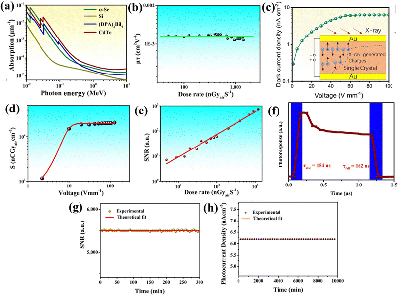 |
| | Fig. 15 (a) Comparison of absorption coefficients of (DPA)2BiI9 with Si, CdTe and α-Se as photon energy functions and (b) μτ product of (DPA)2BiI9 along the c-axis. (c) Idark density versus voltage (inset: vertical structure of the X-ray device); (d) X-ray sensitivities versus voltage; (e) SNR value with respect to dose rates; (f) response time of the on and off states; (g) SNR value from stability test and (h) long-term X-ray photocurrent stability test. Reprinted with permission from ref. 194. Copyright 2023 @ The Royal Society of Chemistry. | |
4.3.2. Thin/thick films. In 2018, renowned research group of H. Li and colleagues developed a composite film of Cs2AgBiBr6 for the purpose of X-ray detection.196 They synthesized the film by adopting a facile method, where a mixture of CsBr, AgBr and BiBr3 and polymers containing hydroxyl functional groups were dissolved in DMSO. Subsequently, the solution was poured onto a glass substrate and dehydrated in a vacuum oven at 150 °C for h. They claimed that the film could be bent up to a radius of 2 mm without degrading its performance. The high resistivity of the composite film was observed to be 2 × 10¹¹ Ω cm. In addition, they conducted a sensitivity test for the Au/perovskite film/Au device under X-ray irradiation from a copper X-ray tube at 45 kV. The sensitivity of the radiation sensor was determined to be 40 μC Gy−1 cm−2, which is greater than that of conventional detectors such as α-Se. Two years later, in 2020, the research group of H. Zhang synthesized an all-inorganic Cs2AgBiBr6 film via the spin-coating technique.197 To obtain the best-quality film, they optimized the dripping time of the anti-solvent isopropanol during spin coating, which was 60 s. Subsequently, a high-film quality was attained with a large electron–hole diffusion length of ∼700 nm and a long carrier lifetime of ∼750 ns. They also carried out a performance test under the illumination of Bremsstrahlung radiation from a tungsten anode X-ray tube with a photon energy of up to 100 keV. The sensitivity and LDDR of the device were 1.8 × 10⁴ μC Gy−1 cm−2 and 145.2 nGy s−1 under a biasing voltage of 5 V, respectively. The research group claimed that their encapsulated device demonstrated a better performance even after two months. As a part of another endeavor, in 2021, Y. Haruta and research team fabricated a 92 μm-thick Cs2AgBiBr6 film with columnar grains via a mist deposition method, which is an ultrasonic-assisted spray deposition method.198 They also revealed the secret formula for columnar growth, which is the redissolution capability of the precursor solution. In addition, the resistivity of the film was assessed to be 1 × 10¹⁰ Ω cm as expected for high-energy radiation sensing. The configuration of X-ray detector was of W/Cs2AgBiBr6/Pt. They also performed a sensitivity test and the obtained sensitivity of the device was 487 μC Gy−1 cm−2 under the biasing electric field of 109 V mm−1. In 2022, another initiative, led by S. Dong, was conducted for synthesizing X-ray detectors by adopting an OIH lead-free perovskite material. They fabricated a perovskite film of MA3Bi2I9 by adopting a very facile technique named the doctor blade coating process for direct conversion X-ray energy.38 They also added MACl as an additive to make the crystal growth rate sluggish to reduce the unexpected formation of pinholes within the film. Consequently, they obtained the best μτ with the addition of 10% MACl with values of 1.62 × 10⁻⁶ cm2 V−1 and 1.17 × 10⁻⁶ cm2 V−1 for holes and electrons, respectively. In addition, the resistivity of the film was observed to be 3.38 × 10¹¹ Ω cm. Moreover, the sensitivity and LDDR of the device were 100.16 μC Gy−1 cm−2 and 98.4 nGy s−1, respectively under the biasing electric field of −3000 V cm−1. Finally, in 2023, the prominent research group led by K. Qin prepared two lead-free films of Cs2AgBiBr6 by means of spin coating utilizing the conventional annealing method and polyimide (PI) tape-assisted annealing method.199 Present, most post-treatments rely on non-contact treatments, which may limit the benefit because the impact on the perovskites induced by direct contact is considerably more straightforward. Due to the strong heat resistance and low glue residual of the PI tape, they offered an annealing method with straightforward manipulation in a solvent environment with the support of PI tape for the perovskite layer post-treatment. It directly influences the perovskite, demonstrating the possibility of direct manipulation by operators, stimulating the recrystallization of the perovskite grains, and eliminating impurity substances. They performed the space-charge-limited current measurements on the two perovskite layers to estimate the trap density. They found that the trap density by the PI method was approximately 20% less than the conventional one, which proved the better crystallinity. In addition, they also observed a greater X-ray absorption coefficient for Cs2AgBiBr6 in comparison with commercial X-ray detectors such as Si, CdTe, and α-Se. Their implemented device structure was SiO2–Ti–Au/Cs2AgBiBr6/PI with an effective area of 0.0021 cm−2. The device with the PI-assisted Cs2AgBiBr6 film exhibited a high X-ray sensitivity of 7.5 × 10⁴ μC Gy−1 cm−2 and LDDR of 47 nGy s−1, which are comparable to all commercial and advanced Pb-based perovskite X-ray detectors. The entire procedure of film development, characterization, and X-ray detection is depicted in Fig. 16.
 |
| | Fig. 16 (a and b) Top-view SEM images of Cs2AgBiBr6 films with different scales: films were fabricated via traditional annealing and PI tape-assisted annealing methods; (c) cross-sectional SEM images of the films; (d) statistics for the distribution of the perovskite crystal grain size with different annealing techniques; (e) AFM image of the PI-assisted film with the RMS (schematic diagram of annealing in inset); (f) comparison of AFM images prepared by PI-assisted techniques (upper) and conventional methods (lower) with their RMS; (g and h) I–V relation of different films and the matching result (schematic illustration of the device in inset); (i) absorption coefficient for various X-ray energies of different materials; (j) current change with different dose rates of X-rays; (k) sensitivity and SNR of the PI-assisted film at different dose rates of X-rays; (l and m) I–T response of the detector under 47 nGy s−1 and 470 nGy s−1, respectively; and (n) comparison of numerous X-ray detectors such as commercial ones and other perovskites. Reprinted with permission from ref. 199. Copyright 2023 @ the American Chemical Society. | |
4.3.3. Wafers. In 2020, the renowned research group of S. Tie and colleagues fabricated a wafer pellet for X-ray radiation detection using green MA3Bi2I9 perovskite with the help of the cold isostatic-pressing technique.200 The pellet displayed a high resistivity of 2.28 × 10¹¹ Ω cm and high balanced mobility of ∼2 cm2 V−1 s−1 for electrons and holes, which are crucial for low noise and weak X-ray detection by X-ray detectors. Subsequently, a high μτ product of the wafer was obtained with a value of 4.6 × 10⁻⁵ cm2 V−1. Finally, they conducted the performance analysis for the configuration of Au/MA3Bi2I9/Au. The LDDR of the device was 9.3 nGy s−1. In addition, the sensitivity towards X-rays reached 563 μC Gy−1 cm−3 under a 2100 V cm−1 bias field, which was 28-times larger than that of the α-Se radiation sensor functioning at a high biasing field of 100000 V cm−1. The prominent research group led by W. Li adopted an approach to build a wafer-type radiation detector by combining Cs2AgBiBr6 perovskite with the (C38H34P2)MnBr4 scintillator through a fast tableting processes in 2021.201 Basically, (C38H34P2)MnBr4 decreased the Idark and noise of the device and enhanced its operating stability by blocking the migration routes of the Cs2AgBiBr6 ions at the grain boundaries. They also provided a path for the functioning of the device while avoiding undesirable light scattering, self-absorption, and even afterglow effects of scintillators. Particularly, the majority of the charges produced by (C38H34P2)MnBr4 were transported to the nearby Cs2AgBiBr6, and then recombined to emit light through scintillation. This light was then again absorbed by the neighboring Cs2AgBiBr6 structure and further induced collectable charge carriers for indirect X-ray detection. The resistivity and μτ product of the hybrid wafer were 8 × 10¹¹ Ω cm and 8.5 × 10⁻⁵ cm2 V−1, respectively. With an LDDR of 0.2 μGy s−1 and a high sensitivity of 114 μC Gy−1 cm−2 under hard X-rays (120 keV), the hybrid X-ray radiation detector exhibited a 75-times lower LDDR than the (C38H34P2)MnBr4 scintillator. In 2022, another research team of C. Zhang developed two X-ray radiation sensors with the configuration of vertical Au/Cs3Bi2I9/Au.202 To fabricate the Cs3Bi2I9 wafer, they utilized two methods. In the first method, DMSO and DMF component solvents (DMSO:DMF = 7:3) were used to dissolve CsI and BiI3 at a mole ratio of 3:2. This mixture was immediately stirred and left at room temperature for 12 h. Then the clear saturated solution was filtered through a PVDF filter (0.8 μm) into the anti-solvent isopropyl IPA. Later, they centrifuged the orange turbid liquid and removed the supernatant liquid and added the necessary amount of IPA to the centrifuge tube. The sediment was then dried for 12 h under a vacuum. According to process two, CsI and BiI3 were combined in an agate jar with agate balls using the same mole ratio and milled for 8 h. The powders were also made using the aforementioned technique. The Cs3Bi2I9 wafer with the first method exhibited higher resistivity (2.21 × 10⁹ Ω cm) than that of the Cs3Bi2I9 wafer obtained with the second method (5.13 × 10⁸ Ω cm). Consequently, the X-ray radiation detector based on the anti-solvent-treated Cs3Bi2I9 wafer displayed better sensitivity and lower detection limit (sensitivity of 588 μC Gy s−1 cm−2 and LDDR of 76 nGy s−1) than that of the HEBM (second method)-based Cs3Bi2I9 wafer (sensitivity of 543 μC Gy s−1 cm−2 and LDDR of 155 nGy s−1) under a biasing electric field of 28.8 V mm−1.Our investigation of the literature indicated that many researchers have suggested substituting conventional X-ray detectors including α-Se, CdTe, Bi2O3, InSe, and TIPS with X-ray detectors based on perovskite materials.119–122,124,126,127,131,133 This shift is motivated by the superior X-ray attenuation ratio, heightened defect tolerance, extended carrier lifetime, and increased electron–hole drift length displayed by perovskite materials.203 Furthermore, the usage of emerging perovskite materials in X-ray detectors has confirmed the enhanced X-ray detection capabilities at a reduced cost and with minimal environmental influence.
In the initial phase of our investigation on organic–inorganic-based X-ray detectors, our focus on SCs, films, and wafers revealed their superior performance in X-ray detection. Various research groups have emphasized the advantages of employing SC perovskite-based detectors as substitutions for conventional detectors such as α-Se and CdTe in X-ray detection systems. These SC-based detectors displayed overall heightened responsiveness to X-ray irradiation, which is attributed to their exceptional crystalline quality, smooth morphology, high bulk resistivity, low trap density, and adequate thickness for effective X-ray attenuation. In addition to SCs, polycrystalline perovskite-based X-ray detectors, including films and wafers, have also established their enhanced performance in comparison with the widely used detectors such as α-Se and CdTe.147,158. This improvement is attributed to advancements in synthesis methodologies and optimization of materials and device architectures. Our literature review disclosed that the ITC method is a popular route that is being employed by researchers for the fabrication of SCs. Notably, the highest performance was attained by the X-ray detector with an MAPbBr3 SC formed via this approach, displaying a sensitivity of 2.35 × 10⁵ μC Gy−1 cm−2 and LDDR of 15.7 nGy s−1.137 In addition, a successful X-ray image of a hex nut was recorded with this direct-conversion pixelated device. However, the device with the SC of MAPbI3, developed by using the ITC method, exhibited the minimal LDDR, measuring at 2.34 nGy s−1.135 Conversely, for the film-based detectors, ultrasound-assisted crystallization combined with post-hot-pressing technique was employed to fabricate a quasi-monocrystalline thick film of MA0.42FA0.58PbI3, and the device with this film displayed a superior performance with a sensitivity of 1.16 × 10⁶ μC Gy−1 cm−2 and the LDDR of the device was recorded to be 37.4 nGy s−1.147 Notably, the film of FA0.5MA0.5PbI3 made up through the blade-coating method exhibited the minimal LDDR with the value of 1.5 nGy s−1.151 On the contrary, in the case of wafer-based detectors, our study highlighted that the X-ray detector with a wafer of MAPbI3 grown through a one-step heat-assisted high-pressure press scheme displayed a better performance than other wafer-based X-ray detectors, achieving a sensitivity of 1.22 × 10⁵ μC Gy−1 cm−2.155 Nevertheless, the device of the MAPbI3 wafer with the minimal LDDR of 0.22 nGy s−1 was prepared through the mechanical sintering of an independent absorber layer and subsequent incorporation onto a pixelated backplane.156
Alternatively, regarding all-inorganic perovskite-based detectors, X-ray detectors with an SC of CsPbBr2.9I0.1, synthesized using the Bridgman method, which is another popular method for fabrication of SCs, exhibited the highest sensitivity of 6.3 × 10⁴ μC Gy−1 cm−2 among the all-inorganic perovskite-based X-ray detectors and the minimal LDDR of 22 nGy s−1 was recorded for the device by utilizing the SC of CsPbBr3 prepared through the same method.173,175 Conversely, the device with a film of CsPbI2Br, manufactured via the vacuum-deposition technique, demonstrated the highest sensitivity of 1.2 × 10⁶ μC Gy−1 cm−2.180 However, the X-ray detector derived from the film of CsPbBr3:Sr, grown by adopting the anti-solvent method, displayed the minimal LDDR of 0.955 nGy s−1.181 On the contrary, regarding wafer-based X-ray detectors, the device with the CsPbBr3–CsPb2Br5–CsPbIxBr3-x composite wafer, developed through water-assisted co-precipitation and spray coating, unveiled the best sensitivity of 20555.1 μC Gy−1 cm−2 among the wafer-based X-ray detectors.184 However, the device from the wafer of Cs2AgBiBr6–BiOBr, synthesized by employing isostatic pressing, recorded a minimal LDDR of 95.3 nGy s−1.185
In the concluding segment of our review on lead-free perovskite-based detectors, the X-ray detector employing an SC of Cs3Bi2I9, developed using a solution evaporation process, demonstrated an outstanding performance, attaining a sensitivity of 59464.4 μC Gy−1 cm−2 and the LDDR was recorded to be 13.5 nGy s−1.192 However, another SC-based detector utilizing CsCu2I3 exhibited the minimal LDDR of 0.93 nGy s−1.186 Conversely, among the lead-free film-based detectors, the X-ray detector utilizing a film of Cs2AgBiBr6, grown through spin-coating, displayed the best performance with a sensitivity of 7.5 × 10⁴ μC Gy−1 cm−2 and the minimal LDDR also was observed at 47 nGy s−1 by the same device.199 On the contrary, in the field of lead-free perovskite wafer-based detectors, the device with the Cs3Bi2I9 wafer prepared through anti-solvent treatment and pressing (24 tons) showed the best sensitivity of 588 μC Gy−1 cm−2 among the lead-free wafer-based detectors, while the MA3Bi2I9-based detector displayed the minimal LDDR of 9.3 nGy s−1.200,202
Our data analysis specified that organic–inorganic X-ray radiation detectors exhibited superior performances in terms of sensitivity, LDDR, and imaging compared to all-inorganic and lead-free perovskite-based X-ray detectors. Alternatively, very few studies suggested that film-based X-ray detectors demonstrated the highest sensitivity in the case of organic–inorganic, all-inorganic, and lead-free perovskite detectors. However, most researchers reported that SC perovskite-based detectors displayed the best performance. Interestingly, wafer-based detectors exhibited poor performances, particularly in the case of lead-free perovskite materials. The superiority of single crystallization techniques lies in the fact that devices based on SCs display a lower trap density, higher resistivity, increased carrier mobility, and longer carrier lifetime in comparison with film and wafer-based X-ray detectors. Consequently, SC-based devices revealed exceptional sensitivity and LDDR. These outcomes exceeded the performance of some conventional commercial X-ray radiation detectors such as amorphous selenium and CZT-based X-ray detectors. Alternatively, the limited performance of film-based devices is attributed to the formation of defects in the bulk film, surfaces, and grain boundaries. Conversely, the wafer-based devices unveiled the poorest performances due to the creation of voids, which inhibit the movement of charge carriers. It is worth noting that various research groups achieved high-performance devices with enhanced stability through the modification of synthesis methods, compositional engineering, and device architectures. However, although the removal of lead addresses environmental concerns, lead-free perovskite based detectors demonstrated relatively inferior performances compared to other types of perovskite-based detectors. Thus, further investigation is essential to comprehend why lead-free perovskite materials demonstrated relatively poorer performances.
Halide perovskites have shown promising developments in X-ray detection, but several challenges remain that must be addressed for their wide-ranging commercial applications. Addressing these challenges should focus on enhancing the stability of materials, improving fabrication methods to attain a uniform perovskite layer with reduced trap density and cost-effectiveness. In addition, it is necessary to explore large-area flexible X-ray detection technology, aiming to improve the sensitivity and lower detection limits. Tackling these challenges is crucial for motivating the future advancements in this field. Some measures may be executed to boost the overall performance of the devices. These include fabricating low-dimensional perovskite materials, incorporating passivated layers or interfacial design to mitigate the impact of ionic migration, developing X-ray radiation detectors based on inorganic perovskites for relatively high stability, optimizing structural design and fabrication methods, adopting low-dimensional perovskite resources in conjunction with 0D/1D/2D materials, optimizing perovskite materials with a high atomic number, and improving film deposition techniques. Additionally, fabricating perovskite SCs requires careful attention to the challenges associated with perovskite films and wafers. Although some studies have addressed these aspects, further research is necessary before implementing these strategies on a broad scale in the field of X-ray detection. A comparative study in tabular form among single crystals, thin/thick film, and wafer-based devices is provided in Table 5.
Table 5 Summary of various parameters in the development of different types of perovskite-based radiation sensors
| |
Device fabricated with |
| Single crystal |
Thin/thick film |
Wafer |
| Fabrication method |
This type of perovskite material was fabricated using some established methods such as inverse-temperature crystallization75,76 temperature-lowering crystallization,82 slow solvent evaporation method,90 anti-solvent vapor-assisted crystallization,92 and Bridgman synthesis method102 |
Thin/thick film-type perovskite materials were fabricated using several conventional methods including the spin coating process,103–105 spray deposition process,107 inkjet printing method,111 and doctor blade method114 |
It is a limited fabrication technique. The common technique is an isostatic-pressing method182 |
| Size and cost |
Forming large-size single crystals of perovskite poses challenges including controlling the crystal growth rate, time-consuming preparation, and incapability for realizing flexible devices81,204 |
Fabricating large-scale films is comparatively straightforward, involving shorter preparation times and yielding sizable, wearable devices205 |
Developing large-sized wafers is also a challenging task |
| Quality |
Achieving single crystals with minimal cracks has been successful64 |
Film quality surpasses that of wafers, but fewer single crystals are observed64 |
The perovskite layer quality is relatively poor |
| Trap density |
Crystals with relatively low trap density have been observed. The lowest trap density was 8.22 × 108 cm−3 (ref. 134) |
Trap density in film is lower than in wafers but higher than in single crystals. The trap density reached its minimum at 1.5 × 1010 cm−3 (ref. 206) |
The perovskite layers exhibit the highest trap density. The exceptional result has also been observed such as one research group reported the lowest trap density of 6 × 108 cm−3 (ref. 149) |
| Mobility–lifetime product |
Relatively high mobility–lifetime products (μτ) have been witnessed. In addition, the observed highest μτ was 1.847 × 10⁻² cm2 V−1 (ref. 183) |
A high mobility–lifetime product has been attained. Furthermore, the recorded highest μτ was 1.32 × 10⁻² cm2 V−1 (ref. 174) |
A relatively poor mobility–lifetime product has been reported. Furthermore, the highest observed μτ was 5.51 × 10⁻³ cm2 V−1 (ref. 182) |
| Sensitivity |
The average sensitivity of the devices has been observed as the highest. Individually, one research group has attained as high as 2.35 × 10⁵ μC Gy−1 cm−2 (ref. 134) |
The average sensitivity in film lies between wafers and single crystal-based devices, with a level higher than that of wafers but lower than that of single crystals. Few exceptional results were also observed in the case of film-based devices such as one research group achieved the highest sensitivity of 1.2 × 10⁶ μC Gy−1 cm−2 (ref. 177) |
Relatively poor sensitivity has been achieved. Individually, one research group accomplished as high as 1.22 × 10⁵ μC Gy−1 cm−2 (ref. 152) |
| LDDR |
Overall, a reduced LDDR has been noted. In addition, one research team reported an LDDR as low as 0.93 nGy s−1 (ref. 183) |
Overall, a lower LDDR has been achieved. In addition, one research team stated an LDDR as low as 0.955 nGy s−1 (ref. 178) |
A relatively high LDDR has been achieved. In addition, exceptional results were also observed. One research team stated an LDDR as low as 0.22 nGy s−1 (ref. 153) |
| Image |
Very few studies conducted the image recording performance |
Only a handful of studies evaluated the performance of image recording |
Only a few studies assessed the performance of image recording |
| Spatial resolution |
A few studies provided information of the spatial resolution of the images. The highest reported spatial resolution was 10 line pairs per millimeter128 |
Only a few studies offered insights into the spatial resolution of the images. The highest stated spatial resolution was 3.3 line pairs per millimeter147 |
Several studies furnished information regarding the spatial resolution of the images. The highest reported spatial resolution was of 6 line pairs per millimeter153 |
| Stability |
Very few studies conducted a stability test. Stability is not up to the mark for commercialization.187 However, they showed relatively better stability than their film and wafer counterparts64 |
The stability tests were conducted infrequently. The stability does not meet the standards required for commercialization.114 However, the results indicate a higher level of stability compared to wafers and lower than that of crystals64 |
Stability tests seldomly conducted. The stability falls short of the standards required for commercialization.151 However, in general, it shows lower stability than that crystals and films |
5. Anti-perovskite-based radiation detectors
The anti-perovskite material is explained with the stoichiometry formula of M3BA, where, M denotes a cation, and A and B represent different-sized anions.207 Specifically, the B anions are positioned in the center of 6-fold-coordinated octahedra and the A anions are 12-fold coordinated with the M cations. The 3D skeleton structure is made up of corner-sharing BM6 octahedra. Ca3AsN and Ba3BiN are examples of anti-perovskites. In comparison with conventional perovskites, the cations replace anions in the octahedra, and these numerous M site cations form anti-perovskites with unusual physical and chemical features linked to d-spin states/the band structure or ion transportation.208 The conventional perovskites frequently display deficiencies or non-stoichiometry, resulting in intriguing structural types and noteworthy optoelectronic features. Oxygen-deficient brownmillerite CaFeO2.5 and LaNiO2.5, as well as ReO3-type compounds (A site unoccupied), are common examples. Similarly, in 2017, the well-known research group led by Y. He reported the vapor transport synthesis of Hg3Q2I2 (Q = S, Se, and Te) SCs with an anti-perovskite structure.207 The Hg3Q2I2 SC structure was defective an anti-perovskite with the stoichiometry formula of Hg6Q2X2, where 50% of the Hg atoms were absent to give the Hg3Q2X2 composition.209 These compounds have a high density (>7 g cm−3) and broad bandgaps (>1.9 eV), resulting in excellent hard radiation-stopping power and a high inherent electrical resistivity of over 1011 Ω cm. In addition, the μτ product for Hg3Q2I2 detectors was achieved in the range of 10−5 cm2 V−1 to 10−6 cm2 V−1. These intriguing characteristics are required in high-energy radiation detection and imaging. As a part of another initiative, the research group led by W. Lin prepared centimeter-size TlSn2I5 2D SCs by the Bridgman method for use in radiation detection devices. In comparison with MAPbX3 (X = Br, I), the anti-perovskite TlSn2I5 showed higher long-term stability, higher photon stopping power (average atomic number of 55), higher resistivity (∼1010 Ω cm), and robust mechanical properties. In addition, the device μτ product was estimated to be 1.1 × 10⁻³ cm2 V−1. Moreover, the device detected the radiation of Kα from Ag X-rays (22 keV), γ from 57Co (122 keV), and α-particles from 241Am (5.5 MeV). These features indicate that anti-perovskite materials are prospective candidates for radiation detection.
6. Conclusion
Perovskite materials have been extensively explored as X-ray radiation detectors for a wide range of applications in the fields of medical imaging, non-destructive industrial inspection, and safety screening. Chronologically, we conducted an extensive review to infer the current scenario of X-ray detection by OIH, all-inorganic and lead-free perovskite-based SCs, films, and wafers. Particularly, we investigated the innovation and modification of a cost-effective synthesis process, the material evolution, and the device architectural modification. It has been observed that the improvement in crystallization techniques dominated the film and wafer growth techniques. The reason for this superiority of the crystallization techniques is that crystal-based especially SC-based devices display a lower trap density, higher resistivity, large carrier mobility and lifetime compared to film and wafer-based devices. Eventually, the devices with SCs showed outstanding sensitivity and LDDR. These results are much better than that of some traditional commercial X-ray radiation detectors such as amorphous selenium- and CZT-based X-ray radiation detectors. In addition, the reasons for the limited device performance of film-based devices include defect formation in the bulk film, surfaces, and grain boundaries. However, wafer-based devices show a lower performance because of the formation of voids, which impede the transportation of charge carriers. We also observed that by performing structural modification, various research groups achieved high-performance devices together with stability. However, although the advancements in perovskite materials and devices for X-ray radiation detection have displayed promising performances, they still face critical challenges for real-world applications. These problems can be resolved by increasing the material stability, improving the fabrication techniques to obtain uniform, lower trap density and cost-effective perovskite layers, and investigating large-area flexible X-ray detection technology with improved sensitivity and lower detection limits. Thus, addressing these challenges is essential for future innovations in this field. Some measures may be executed to boost the overall performance of the devices including preparing low-dimensional perovskite materials, using passivated layers or interfacial design to reduce the effect of ion migration, producing inorganic perovskite-based X-ray radiation detectors, optimizing structural design and fabrication methods, using low-dimensional perovskite resources in conjunction with 0D/1D/2D materials, optimizing perovskites with a high atomic number and improving film deposition methods, and fabricating perovskite SCs by paying closer attention to the hurdles regarding perovskite films and perovskite wafers. However, although there have been some studies on this matter, much more study is required before it can be adopted in X-ray detection. We should maintain an optimistic mindset as well as devise distinctive strategies to bring them to market.
Consent for publication
All authors of this work have agreed and are ready to sign the Transfer of Copyright which empowers the Publisher to protect the work against unauthorized use and to maintain the integrity of the work from a bibliographical and archival standpoint.
Data availability
All data are available in the manuscript.
Author contributions
M. H. M. developed the concept and wrote the main manuscript, M. U. K., M. A. I., M. N. A., H. O. and M. H. U. reviewed the manuscript, M. U. K. Supported the theoretical methodology and computational packages, M. U. K., M. A. I., M. N. A., H. O. and M. H. U. provided technical, theoretical and conceptual reviews.
Conflicts of interest
The authors declare that they have no known competing financial interests or personal relationships that could have appeared to influence the work reported in this paper.
Acknowledgements
Mr. Md. Helal Miah expresses gratitude to Sunway University for generously awarding him a fully funded scholarship to pursue his Ph.D. studies.
References
- S. O. Kasap, M. Zahangir Kabir and J. A. Rowlands, Recent advances in X-ray photoconductors for direct conversion X-ray image detectors, Curr. Appl. Phys., 2006, 6(3), 288–292, DOI:10.1016/J.CAP.2005.11.001.
- Y. Yang, Y. Su, W. Ma and Y. M. Yang, Perovskite semiconductors for direct X-ray detection and imaging, J. Semicond., 2020, 41(5), 051204, DOI:10.1088/1674-4926/41/5/051204.
- A. Bernheim, et al., Chest CT findings in coronavirus disease 2019 (COVID-19): Relationship to duration of infection, Radiology, 2020, 295(3), 685–691, DOI:10.1148/RADIOL.2020200463/ASSET/IMAGES/LARGE/RADIOL.2020200463.FIG5B.JPEG.
- H. Hu, L. Shen, Q. Guan, X. Li, Q. Zhou and S. Ruan, Deep co-supervision and attention fusion strategy for automatic COVID-19 lung infection segmentation on CT images, Pattern Recognit., 2022, 124, 108452, DOI:10.1016/J.PATCOG.2021.108452.
- F. Y. Zhang, Y. Qiao and H. Zhang, CT imaging of the COVID-19, J. Formosan Med. Assoc., 2020, 119(5), 990–992, DOI:10.1016/J.JFMA.2020.04.006.
- A. T. Chen, G. B. Coura-Filho and M. H. Rehder, Clinical Characteristics of Covid-19 in China, N. Engl. J. Med., 2020, 382(19), 1859–1862, DOI:10.1056/NEJMC2005203.
- M. R. Squillante, J. F. Christian and G. Entine, Solid State Radiation Detectors, Wiley Encycl. Electr. Electron. Eng., 2016, 1–18, DOI:10.1002/047134608X.W5214.PUB2.
- R. C. Alig and S. Bloom, Electron-Hole-Pair Creation Energies in Semiconductors, Phys. Rev. Lett., 1975, 35(22), 1522–1525, DOI:10.1103/PHYSREVLETT.35.1522.
- J. Iguaz, et al., Energy resolution of alpha particles in a Micromegas detector at high pressure, J. Phys.: Conf. Ser., 2009, 179(1), 012007, DOI:10.1088/1742-6596/179/1/012007.
- D. S. McGregor, Z. He, H. A. Seifert, D. K. Wehe and R. A. Rojeski, Single charge carrier type sensing with a parallel strip pseudo-Frisch-grid CdZnTe semiconductor radiation detector, Appl. Phys. Lett., 1998, 72(7), 792–794, DOI:10.1063/1.120895.
- C. Sun, et al., Highly luminescent, stable, transparent and flexible perovskite quantum dot gels towards light-emitting diodes, Nanotechnology, 2017, 28(36), 365601, DOI:10.1088/1361-6528/AA7C86.
- H. Hu, G. Niu, Z. Zheng, L. Xu, L. Liu and J. Tang, Perovskite semiconductors for ionizing radiation detection, EcoMat, 2022, 4(6), e12258, DOI:10.1002/EOM2.12258.
- W. Wang, Y. Ma and L. Qi, High-Performance Photodetectors Based on Organometal Halide Perovskite Nanonets, Adv. Funct. Mater., 2017, 27(12), 1603653, DOI:10.1002/ADFM.201603653.
- Y. Eisen and A. Shor, CdTe and CdZnTe materials for room-temperature X-ray and gamma ray detectors, J. Cryst. Growth, 1998, 184–185, 1302–1312, DOI:10.1016/S0022-0248(98)80270-4.
- M. B. Rahman, N.-E. Ashrafi, M. H. Miah, M. U. Khandaker and M. A. Islam, Selection of a compatible electron transport layer and hole transport layer for the mixed perovskite FA0.85Cs0.15Pb (I0.85Br0.15)3, towards achieving novel structure and high-efficiency perovskite solar cells: a detailed numerical study by SCAPS-1D, RSC Adv., 2023, 13(25), 17130–17142, 10.1039/D3RA02170J.
- R. Kumar Singh, N. Jain, S. Som, S. Dutta, J. Singh and R. Kumar, Lead-Free Hybrid Perovskite Light-Harvesting Material for QD-LED Application, Perovskite Materials, Devices and Integration, IntechOpen, 2020, DOI:10.5772/intechopen.86836.
- M. Helal Miah, et al., Optimization and detail analysis of novel structure Pb-free CsGeI3-based all-inorganic perovskite solar cells by SCAPS-1D, Optik, 2023, 281, 170819, DOI:10.1016/J.IJLEO.2023.170819.
- M. Houari, et al., Semiconductor behavior of halide perovskites AGeX3 (A = K, Rb and Cs; X = F, Cl and Br): first-principles calculations, Indian J. Phys., 2020, 94(4), 455–467, DOI:10.1007/S12648-019-01480-0/METRICS.
- Y. Fang, Q. Dong, Y. Shao, Y. Yuan and J. Huang, Highly narrowband perovskite single-crystal photodetectors enabled by surface-charge recombination, Nat. Photonics, 2015, 9(10), 679–686, DOI:10.1038/nphoton.2015.156.
- Q. Chen, et al., Under the spotlight: The organic–inorganic hybrid halide perovskite for optoelectronic applications, Nano Today, 2015, 10(3), 355–396, DOI:10.1016/J.NANTOD.2015.04.009.
- D. W. DeQuilettes, et al., Impact of microstructure on local carrier lifetime in perovskite solar cells, Science, 2015, 348(6235), 683–686, DOI:10.1126/SCIENCE.AAA5333/SUPPL_FILE/AAA5333-DEQUILETTES-SM.PDF.
- M. Liu, M. B. Johnston and H. J. Snaith, Efficient planar heterojunction perovskite solar cells by vapour deposition, Nature, 2013, 501(7467), 395–398, DOI:10.1038/nature12509.
- A. Kojima, K. Teshima, Y. Shirai and T. Miyasaka, Organometal halide perovskites as visible-light sensitizers for photovoltaic cells, J. Am. Chem. Soc., 2009, 131(17), 6050–6051, DOI:10.1021/JA809598R/SUPPL_FILE/JA809598R_SI_001.PDF.
- H. Min, et al., Perovskite solar cells with atomically coherent interlayers on SnO2 electrodes, Nature, 2021, 598(7881), 444–450, DOI:10.1038/s41586-021-03964-8.
- Q. Hu, et al., X-ray scintillation in lead-free double perovskite crystals, Sci. China: Chem., 2018, 61(12), 1581–1586, DOI:10.1007/S11426-018-9308-2/METRICS.
- D. N. Jeong, J. M. Yang and N. G. Park, Roadmap on halide perovskite and related devices, Nanotechnology, 2020, 31(15), 152001, DOI:10.1088/1361-6528/AB59ED.
- L. Gao and Q. Yan, Recent Advances in Lead Halide Perovskites for Radiation Detectors, Sol. RRL, 2020, 4(2), 1900210, DOI:10.1002/SOLR.201900210.
- H. Wei and J. Huang, Halide lead perovskites for ionizing radiation detection, Nat. Commun., 2019, 10(1), 1–12, DOI:10.1038/s41467-019-08981-w.
- P. Büchele, et al., X-ray imaging with scintillator-sensitized hybrid organic photodetectors, Nat. Photonics, 2015, 9(12), 843–848, DOI:10.1038/nphoton.2015.216.
- Y. Haruta, et al., Scalable Fabrication of Metal Halide Perovskites for Direct X-ray Flat-Panel Detectors: A Perspective, Chem. Mater., 2022, 34(12), 5323–5333, DOI:10.1021/ACS.CHEMMATER.2C00764/ASSET/IMAGES/MEDIUM/CM2C00764_0009.GIF.
- Z. Luo, J. G. Moch, S. S. Johnson and C. C. Chen, A Review on X-ray Detection Using Nanomaterials, Curr. Nanosci., 2017, 13(4), 364–372, DOI:10.2174/1573413713666170329164615.
- A. Owens, Semiconductor materials and radiation detection, J. Synchrotron Radiat., 2006, 13(2), 143–150, DOI:10.1107/S0909049505033339.
- R. Bellazzini, G. Spandre, A. Brez, M. Minuti, M. Pinchera and P. Mozzo, Chromatic X-ray imaging with a fine pitch CdTe sensor coupled to a large area photon counting pixel ASIC, J. Instrum., 2013, 8(02), C02028, DOI:10.1088/1748-0221/8/02/C02028.
- J. Guo, et al., Morphology of X-ray detector Cs2TeI6 perovskite thick films grown by electrospray method, J. Mater. Chem. C, 2019, 7(28), 8712–8719, 10.1039/C9TC02022E.
- M. Z. Kabir and S. Kasap, Photoconductors for x-ray image detectors, Springer Handbooks, 2017, p. 1, DOI:10.1007/978-3-319-48933-9_45/COVER.
- G. J. Matt, et al., Sensitive Direct Converting X-Ray Detectors Utilizing Crystalline CsPbBr3 Perovskite Films Fabricated via Scalable Melt Processing, Adv. Mater. Interfaces, 2020, 7(4), 1901575, DOI:10.1002/ADMI.201901575.
- X. Li, et al., Ultralow Detection Limit and Robust Hard X-ray Imaging Detector Based on Inch-Sized Lead-Free Perovskite Cs3Bi2Br9 Single Crystals, ACS Appl. Mater. Interfaces, 2022, 14(7), 9340–9351, DOI:10.1021/ACSAMI.1C24086/SUPPL_FILE/AM1C24086_SI_001.PDF.
- S. Dong, et al., Green solvent blade-coated MA3Bi2I9 for direct-conversion X-ray detectors, J. Mater. Chem. C, 2022, 10(16), 6236–6242, 10.1039/D2TC00522K.
- H. Wei, et al., Sensitive X-ray detectors made of methylammonium lead tribromide perovskite single crystals, Nat. Photonics, 2016, 10(5), 333–339, DOI:10.1038/nphoton.2016.41.
- S. Wu, et al., A Photoconductive X-ray Detector with a High Figure of Merit Based on an Open-Framework Chalcogenide Semiconductor, Angew. Chem., Int. Ed., 2020, 59(42), 18605–18610, DOI:10.1002/ANIE.202010290.
- Z. Li, F. Zhou, H. H. Yao, Z. Ci, Z. Yang and Z. Jin, Halide perovskites for high-performance X-ray detector, Mater. Today, 2021, 48, 155–175, DOI:10.1016/J.MATTOD.2021.01.028.
- W. Shockley, Problems related to p–n junctions in silicon, Czech. J. Phys., 1961, 11(2), 81–121, DOI:10.1007/BF01688613/METRICS.
- W. Pan, et al., Hot-Pressed CsPbBr3 Quasi-Monocrystalline Film for Sensitive Direct X-ray Detection, Adv. Mater., 2019, 31(44), 1904405, DOI:10.1002/ADMA.201904405.
- G. Kakavelakis, M. Gedda, A. Panagiotopoulos, E. Kymakis, T. D. Anthopoulos and K. Petridis, Metal Halide Perovskites for High-Energy Radiation Detection, Adv. Sci., 2020, 7(22), 2002098, DOI:10.1002/ADVS.202002098.
- Š. Uxa, R. Grill and E. Belas, Evaluation of the mobility-lifetime product in CdTe and CdZnTe detectors by the transient-current technique, J. Appl. Phys., 2013, 114(9), 094511, DOI:10.1063/1.4819891/372176.
- J. Ghosh, P. J. Sellin and P. K. Giri, Recent advances in lead-free double perovskites for x-ray and photodetection, Nanotechnology, 2022, 33(31), 312001, DOI:10.1088/1361-6528/AC6884.
- L. Basiricò, A. Ciavatti, B. Fraboni, L. Basiricò, A. Ciavatti and B. Fraboni, Solution-Grown Organic and Perovskite X-Ray Detectors: A New Paradigm for the Direct Detection of Ionizing Radiation, Adv. Mater. Technol., 2021, 6(1), 2000475, DOI:10.1002/ADMT.202000475.
- H. Wei and J. Huang, Halide lead perovskites for ionizing radiation detection, Nat. Commun., 2019, 10(1), 1–12, DOI:10.1038/s41467-019-08981-w.
- L. Basiricò, A. Ciavatti, B. Fraboni, L. Basiricò, A. Ciavatti and B. Fraboni, Solution-Grown Organic and Perovskite X-Ray Detectors: A New Paradigm for the Direct Detection of Ionizing Radiation, Adv. Mater. Technol., 2021, 6(1), 2000475, DOI:10.1002/ADMT.202000475.
- T. Yang, F. Li and R. Zheng, Recent advances in radiation detection technologies enabled by metal-halide perovskites, Mater. Adv., 2021, 2(21), 6744–6767, 10.1039/D1MA00569C.
- C. F. Lin, K. W. Huang, Y. T. Chen, S. L. Hsueh, M. H. Li and P. Chen, Perovskite-Based X-ray Detectors, Nanomaterials, 2023, 13(13), 2024, DOI:10.3390/NANO13132024.
- Y. Fang, A. Armin, P. Meredith and J. Huang, Accurate characterization of next-generation thin-film photodetectors, Nat. Photonics, 2018, 13(1), 1–4, DOI:10.1038/s41566-018-0288-z.
- W. Pan, et al., Cs2AgBiBr6 single-crystal X-ray detectors with a low detection limit, Nat. Photonics, 2017, 11(11), 726–732, DOI:10.1038/s41566-017-0012-4.
- M. Thompson, S. L. R. Ellison and R. Wood, Harmonized guidelines for single-laboratory validation of methods of analysis (IUPAC Technical Report), Pure Appl. Chem., 2002, 74(5), 835–855, DOI:10.1351/PAC200274050835/MACHINEREADABLECITATION/RIS.
- R. Zhuang, et al., Highly sensitive X-ray detector made of layered perovskite-like (NH4)3Bi2I9 single crystal with anisotropic response, Nat. Photonics, 2019, 13(9), 602–608, DOI:10.1038/s41566-019-0466-7.
- X. Zheng, et al., Ultrasensitive and stable X-ray detection using zero-dimensional lead-free perovskites, J. Energy Chem., 2020, 49, 299–306, DOI:10.1016/J.JECHEM.2020.02.049.
- Y. Yang, Y. Su, W. Ma and Y. M. Yang, Perovskite semiconductors for direct X-ray detection and imaging, J. Semicond., 2020, 41(5), 051204, DOI:10.1088/1674-4926/41/5/051204.
- G. A. Elbaz, et al., Unbalanced Hole and Electron Diffusion in Lead Bromide Perovskites, Nano Lett., 2017, 17(3), 1727–1732, DOI:10.1021/ACS.NANOLETT.6B05022/SUPPL_FILE/NL6B05022_SI_003.CIF.
- W. Heiss and C. Brabec, Perovskites target X-ray detection, Nat. Photonics, 2016, 10(5), 288–289, DOI:10.1038/nphoton.2016.54.
- W. Pan, et al., Cs2AgBiBr6 single-crystal X-ray detectors with a low detection limit, Nat. Photonics, 2017, 11(11), 726–732, DOI:10.1038/s41566-017-0012-4.
- L. Li, et al., An Electrically Modulated Single-Color/Dual-Color Imaging Photodetector, Adv. Mater., 2020, 32(24), 1907257, DOI:10.1002/ADMA.201907257.
- Y. Liu, et al., Large Lead-Free Perovskite Single Crystal for High-Performance Coplanar X-Ray Imaging Applications, Adv. Opt. Mater., 2020, 8(19), 2000814, DOI:10.1002/ADOM.202000814.
- J. Xu, et al., Progress of Metal Halide Perovskite Crystals from a Crystal Growth Point of View, Cryst. Res. Technol., 2023, 58(1), 2200128, DOI:10.1002/CRAT.202200128.
- J. Yu, et al., Perovskite CsPbBr3 crystals: growth and applications, J. Mater. Chem. C, 2020, 8(19), 6326–6341, 10.1039/D0TC00922A.
- J. Yin, Q. Lei, Y. Han, O. M. Bakr and O. F. Mohammed, Luminescent Copper(I) Halides for Optoelectronic Applications, Phys. Status Solidi RRL, 2021, 15(12), 2100138, DOI:10.1002/PSSR.202100138.
- X. Wang, et al., Solution-Processed Halide Perovskite Single Crystals with Intrinsic Compositional Gradients for X-ray Detection, Chem. Mater., 2020, 32(12), 4973–4983, DOI:10.1021/ACS.CHEMMATER.9B05000/SUPPL_FILE/CM9B05000_SI_001.PDF.
- C. C. Stoumpos, et al., Crystal growth of the perovskite semiconductor CsPbBr3: A new material for high-energy radiation detection, Cryst. Growth Des., 2013, 13(7), 2722–2727, DOI:10.1021/CG400645T.
- X. Qin, Y. Yao, H. Dong, Y. Zhen, L. Jiang and W. Hu, Perovskite Photodetectors based on CH3NH3PbI3 Single Crystals, Chem.–Asian J., 2016, 11(19), 2675–2679, DOI:10.1002/ASIA.201600430.
- H. Wang and D. H. Kim, Perovskite-based photodetectors: materials and devices, Chem. Soc. Rev., 2017, 46(17), 5204–5236, 10.1039/C6CS00896H.
- B. Fraboni, A. Fraleoni-Morgera and N. Zaitseva, Ionizing Radiation Detectors Based on Solution-Grown Organic Single Crystals, Adv. Funct. Mater., 2016, 26(14), 2276–2291, DOI:10.1002/ADFM.201502669.
- Y. Li, H. Sun, Y. Shi and K. Tsukagoshi, Patterning technology for solution-processed organic crystal field-effect transistors, Sci. Technol. Adv. Mater., 2014, 15(2), 024203, DOI:10.1088/1468-6996/15/2/024203.
- C. C. Stoumpos, et al., Crystal growth of the perovskite semiconductor CsPbBr3: A new material for high-energy radiation detection, Cryst. Growth Des., 2013, 13(7), 2722–2727, DOI:10.1021/CG400645T/SUPPL_FILE/CG400645T_SI_002.CIF.
- Y. Dang, D. Ju, L. Wang and X. Tao, Recent progress in the synthesis of hybrid halide perovskite single crystals, CrystEngComm, 2016, 18(24), 4476–4484, 10.1039/C6CE00655H.
- L. Basiricò, A. Ciavatti, B. Fraboni, L. Basiricò, A. Ciavatti and B. Fraboni, Solution-Grown Organic and Perovskite X-Ray Detectors: A New Paradigm for the Direct Detection of Ionizing Radiation, Adv. Mater. Technol., 2021, 6(1), 2000475, DOI:10.1002/ADMT.202000475.
- S. Yakunin, et al., Detection of gamma photons using solution-grown single crystals of hybrid lead halide perovskites, Nat. Photonics, 2016, 10(9), 585–589, DOI:10.1038/nphoton.2016.139.
- Y. Liu, et al., Inch-Size 0D-Structured Lead-Free Perovskite Single Crystals for Highly Sensitive Stable X-Ray Imaging, Matter, 2020, 3(1), 180–196, DOI:10.1016/J.MATT.2020.04.017.
- Y. Liu, et al., Ligand assisted growth of perovskite single crystals with low defect density, Nat. Commun., 2021, 12(1), 1–8, DOI:10.1038/s41467-021-21934-6.
- J. Peng, et al., Crystallization
of CsPbBr3 single crystals in water for X-ray detection, Nat. Commun., 2021, 12(1), 1–10, DOI:10.1038/s41467-021-21805-0.
- J. Peng, et al., Crystallization of CsPbBr3 single crystals in water for X-ray detection, Nat. Commun., 2021, 12(1), 1–10, DOI:10.1038/s41467-021-21805-0.
- L. Carman, et al., Solution-Grown Rubrene Crystals as Radiation Detecting Devices, IEEE Trans. Nucl. Sci., 2017, 64(2), 781–788, DOI:10.1109/TNS.2017.2652139.
- X. Song, et al., Metal-Free Halide Perovskite Single Crystals with Very Long Charge Lifetimes for Efficient X-ray Imaging, Adv. Mater., 2020, 32(42), 2003353, DOI:10.1002/ADMA.202003353.
- W. Yuan, et al., In Situ Regulating the Order–Disorder Phase Transition in Cs2AgBiBr6 Single Crystal toward the Application in an X-Ray Detector, Adv. Funct. Mater., 2019, 29(20), 1900234, DOI:10.1002/ADFM.201900234.
- A. Fraleoni-Morgera, L. Benevoli and B. Fraboni, Solution growth of single crystals of 4-hydroxycyanobenzene (4HCB) suitable for electronic applications, J. Cryst. Growth, 2010, 312(23), 3466–3472, DOI:10.1016/J.JCRYSGRO.2010.08.057.
- W. Nie, et al., High-efficiency solution-processed perovskite solar cells with millimeter-scale grains, Science, 2015, 347(6221), 522–525, DOI:10.1126/SCIENCE.AAA0472/SUPPL_FILE/NIE.SM.PDF.
- L. Basirico, et al., Solid State Organic X-Ray Detectors Based on Rubrene Single Crystals, IEEE Trans. Nucl. Sci., 2015, 62(4), 1791–1797, DOI:10.1109/TNS.2015.2456418.
- B. Fraboni, et al., Organic Semiconducting Single Crystals as Next Generation of Low-Cost, Room-Temperature Electrical X-ray Detectors, Adv. Mater., 2012, 24, 2289–2293, DOI:10.1002/adma.201200283.
- B. Fraboni, A. Ciavatti, L. Basiricò and A. Fraleoni-Morgera, Organic semiconducting single crystals as solid-state sensors for ionizing radiation, Faraday Discuss., 2014, 174, 219–234, 10.1039/C4FD00102H.
- A. Ciavatti, et al., Toward Low-Voltage and Bendable X-Ray Direct Detectors Based on Organic Semiconducting Single Crystals, Adv. Mater., 2015, 27(44), 7213–7220, DOI:10.1002/ADMA.201503090.
- A. Ciavatti, P. J. Sellin, L. Basiricò, A. Fraleoni-Morgera and B. Fraboni, Charged-particle spectroscopy in organic semiconducting single crystals, Appl. Phys. Lett., 2016, 108(15), 153301, DOI:10.1063/1.4945597/30693.
- W. Guo, et al., Room-Temperature Ferroelectric Material Composed of a Two-Dimensional Metal Halide Double Perovskite for X-ray Detection, Angew. Chem., Int. Ed., 2020, 59(33), 13879–13884, DOI:10.1002/ANIE.202004235.
- D. Shi, et al., Low trap-state density and long carrier diffusion in organolead trihalide perovskite single crystals, Science, 2015, 347(6221), 519–522, DOI:10.1126/SCIENCE.AAA2725/SUPPL_FILE/SHI.SM.PDF.
- H. Wei, et al., Sensitive X-ray detectors made of methylammonium lead tribromide perovskite single crystals, Nat. Photonics, 2016, 10(5), 333–339, DOI:10.1038/nphoton.2016.41.
- Q. Chen, et al., All-inorganic perovskite nanocrystal scintillators, Nature, 2018, 561(7721), 88–93, DOI:10.1038/s41586-018-0451-1.
- Y. Dang, D. Ju, L. Wang and X. Tao, Recent progress in the synthesis of hybrid halide perovskite single crystals, CrystEngComm, 2016, 18(24), 4476–4484, 10.1039/C6CE00655H.
- C. W. Ahn, et al., Highly ordered lead-free double perovskite halides by design, J. Mater., 2020, 6(4), 651–660, DOI:10.1016/J.JMAT.2020.05.008.
- Z. Zeng, et al., Multimodal Luminescent Yb3+/Er3+/Bi3+-Doped Perovskite Single Crystals for X-ray Detection and Anti-Counterfeiting, Adv. Mater., 2020, 32(43), 2004506, DOI:10.1002/ADMA.202004506.
- W. Zhu, et al., Low-dose real-time X-ray imaging with nontoxic double perovskite scintillators, Light: Sci. Appl., 2020, 9(1), 1–10, DOI:10.1038/s41377-020-00353-0.
- Y. He, et al., Defect Antiperovskite Compounds Hg3Q2I2 (Q = S, Se, and Te) for Room-Temperature Hard Radiation Detection, J. Am. Chem. Soc., 2017, 139(23), 7939–7951, DOI:10.1021/JACS.7B03174/SUPPL_FILE/JA7B03174_SI_001.PDF.
- Y. He, et al., Controlling the Vapor Transport Crystal Growth of Hg3Se2I2 Hard Radiation Detector Using Organic Polymer, Cryst. Growth Des., 2019, 19(4), 2074–2080, DOI:10.1021/ACS.CGD.8B01646/SUPPL_FILE/CG8B01646_SI_001.PDF.
- T. Sorgenfrei, F. Hofherr, T. Jauß and A. Cröll, Synthesis and single crystal growth of SnS by the Bridgman-Stockbarger technique, Cryst. Res. Technol., 2013, 48(4), 193–199, DOI:10.1002/CRAT.201200484.
- Q. Chen, et al., All-inorganic perovskite nanocrystal scintillators, Nature, 2018, 561(7721), 88–93, DOI:10.1038/s41586-018-0451-1.
- C. C. Stoumpos, et al., Crystal growth of the perovskite semiconductor CsPbBr3: A new material for high-energy radiation detection, Cryst. Growth Des., 2013, 13(7), 2722–2727, DOI:10.1021/CG400645T.
- L. Basiricò, S. P. Senanayak, A. Ciavatti, M. Abdi-Jalebi, B. Fraboni and H. Sirringhaus, Detection of X-Rays by Solution-Processed Cesium-Containing Mixed Triple Cation Perovskite Thin Films, Adv. Funct. Mater., 2019, 29(34), 1902346, DOI:10.1002/ADFM.201902346.
- A. Ciavatti, et al., Dynamics of direct X-ray detection processes in high-Z Bi2O3 nanoparticles-loaded PFO polymer-based diodes, Appl. Phys. Lett., 2017, 111(18), 183301, DOI:10.1063/1.4986345/34242.
- A. Intaniwet, J. L. Keddie, M. Shkunov and P. J. Sellin, High charge-carrier mobilities in blends of poly(triarylamine) and TIPS-pentacene leading to better performing X-ray sensors, Org. Electron., 2011, 12(11), 1903–1908, DOI:10.1016/J.ORGEL.2011.08.003.
- Y. Diao, L. Shaw, Z. Bao and S. C. B. Mannsfeld, Morphology control strategies for solution-processed organic semiconductor thin films, Energy Environ. Sci., 2014, 7(7), 2145–2159, 10.1039/C4EE00688G.
- S. Yakunin, et al., Detection of X-ray photons by solution-processed lead halide perovskites, Nat. Photonics, 2015, 9(7), 444–449, DOI:10.1038/nphoton.2015.82.
- Y. Tan, G. Mu, M. Chen and X. Tang, X-ray Detectors Based on Halide Perovskite Materials, Coatings, 2023, 13(1), 211, DOI:10.3390/COATINGS13010211.
- W. Qian, et al., An aerosol-liquid-solid process for the general synthesis of halide perovskite thick films for direct-conversion X-ray detectors, Matter, 2021, 4(3), 942–954, DOI:10.1016/J.MATT.2021.01.020.
- Z. Gou, et al., Self-Powered X-Ray Detector Based on All-Inorganic Perovskite Thick Film with High Sensitivity Under Low Dose Rate, Phys. Status Solidi RRL, 2019, 13(8), 1900094, DOI:10.1002/PSSR.201900094.
- J. Liu, et al., Flexible, Printable Soft-X-Ray Detectors Based on All-Inorganic Perovskite Quantum Dots, Adv. Mater., 2019, 31(30), 1901644, DOI:10.1002/ADMA.201901644.
- M. Duan, et al., Inkjet-Printed Micrometer-Thick Patterned Perovskite Quantum Dot Films for Efficient Blue-to-Green Photoconversion, Adv. Mater. Technol., 2019, 4(12), 1900779, DOI:10.1002/ADMT.201900779.
- Y. C. Kim, et al., Printable organometallic perovskite enables large-area, low-dose X-ray imaging, Nature, 2017, 550(7674), 87–91, DOI:10.1038/nature24032.
- J. Tan, et al., Self-powered X-ray detector based on lead halide perovskites under electric field poling effect, J. Mater. Sci.: Mater. Electron., 2023, 34(15), 1–11, DOI:10.1007/S10854-023-10627-Z.
- I. Temiño, et al., Morphology and mobility as tools to control and unprecedentedly enhance X-ray sensitivity in organic thin-films, Nat. Commun., 2020, 11(1), 1–10, DOI:10.1038/s41467-020-15974-7.
- X. Xu, et al., Light Management of Metal Halide Scintillators for High-Resolution X-Ray Imaging, Adv. Mater., 2024, 36(3), 2303738, DOI:10.1002/ADMA.202303738.
- Y. Wang, M. Li, Z. Chai, Y. Wang and S. Wang, Perovskite Scintillators for Improved X-ray Detection and Imaging, Angew. Chem., Int. Ed., 2023, 62(38), e202304638, DOI:10.1002/ANIE.202304638.
- A. Wibowo, et al., Development and challenges in perovskite scintillators for high-resolution imaging and timing applications, Commun. Mater., 2023, 4(1), 1–10, DOI:10.1038/s43246-023-00348-5.
- S. O. Kasap, X-ray sensitivity of photoconductors: application to stabilized a-Se, J. Phys. D Appl. Phys., 2000, 33(21), 2853, DOI:10.1088/0022-3727/33/21/326.
- S. Kasap, et al., Amorphous and Polycrystalline Photoconductors for Direct Conversion Flat Panel X-Ray Image Sensors, Sensors, 2011, 11(5), 5112–5157, DOI:10.3390/S110505112.
- H. M. Thirimanne, et al., High sensitivity organic inorganic hybrid X-ray detectors with direct transduction and broadband response, Nat. Commun., 2018, 9(1), 2926, DOI:10.1038/s41467-018-05301-6.
- L. Basiricò, A. Ciavatti, T. Cramer, P. Cosseddu, A. Bonfiglio and B. Fraboni, Direct X-ray photoconversion in flexible organic thin film devices operated below 1 V, Nat. Commun., 2016, 7, 13063, DOI:10.1038/ncomms13063.
- I. Temiño, et al., Morphology and mobility as tools to control and unprecedentedly enhance X-ray sensitivity in organic thin-films, Nat. Commun., 2020, 11(1), 2136, DOI:10.1038/s41467-020-15974-7.
- S. Wu, et al., A Photoconductive X-ray Detector with a High Figure of Merit Based on an Open-Framework Chalcogenide Semiconductor, Angew. Chem., Int. Ed., 2020, 59(42), 18605–18610, DOI:10.1002/ANIE.202010290.
- Y. Huang, et al., A-site Cation Engineering for Highly Efficient MAPbI3 Single-Crystal X-ray Detector, Angew. Chem., Int. Ed., 2019, 58(49), 17834–17842, DOI:10.1002/ANIE.201911281.
- R. Bellazzini, G. Spandre, A. Brez, M. Minuti, M. Pinchera and P. Mozzo, Chromatic X-ray imaging with a fine pitch CdTe sensor coupled to a large area photon counting pixel ASIC, J. Instrum., 2013, 8(02), C02028, DOI:10.1088/1748-0221/8/02/C02028.
- Y. M. Ivanov, et al., The possibilities of using semi-insulating CdTe crystals as detecting material for X-ray imaging radiography, Phys. Status Solidi, 2003,(3), 840–844, DOI:10.1002/PSSC.200306258.
- H. Min, et al., Perovskite solar cells with atomically coherent interlayers on SnO2 electrodes, Nature, 2021, 598(7881), 444–450, DOI:10.1038/s41586-021-03964-8.
- W. Wei, et al., Monolithic integration of hybrid perovskite single crystals with heterogenous substrate for highly sensitive X-ray imaging, Nat. Photonics, 2017, 11(5), 315–321, DOI:10.1038/nphoton.2017.43.
- B. Náfrádi, G. Náfrádi, L. Forró and E. Horváth, Methylammonium Lead Iodide for Efficient X-ray Energy Conversion, J. Phys. Chem. C, 2015, 119(45), 25204–25208, DOI:10.1021/ACS.JPCC.5B07876/ASSET/IMAGES/MEDIUM/JP-2015-078769_0005.GIF.
- W. Wei, et al., Monolithic integration of hybrid perovskite single crystals with heterogenous substrate for highly sensitive X-ray imaging, Nat. Photonics, 2017, 11(5), 315–321, DOI:10.1038/nphoton.2017.43.
- F. Ye, et al., High-Quality Cuboid CH3NH3PbI3 Single Crystals for High Performance X-Ray and Photon Detectors, Adv. Funct. Mater., 2019, 29(6), 1806984, DOI:10.1002/ADFM.201806984.
- Y. Huang, et al., A-site Cation Engineering for Highly Efficient MAPbI3 Single-Crystal X-ray Detector, Angew. Chem., Int. Ed., 2019, 58(49), 17834–17842, DOI:10.1002/ANIE.201911281.
- Z. Fan, et al., Solution-Processed MAPbBr3 and CsPbBr3 Single-Crystal Detectors with Improved X-Ray Sensitivity via Interfacial Engineering, Phys. Status Solidi, 2020, 217(9), 2000104, DOI:10.1002/PSSA.202000104.
- Y. Liu, et al., Ligand assisted growth of perovskite single crystals with low defect density, Nat. Commun., 2021, 12(1), 1–8, DOI:10.1038/s41467-021-21934-6.
- J. Jiang, et al., Synergistic strain engineering of perovskite single crystals for highly stable and sensitive X-ray detectors with low-bias imaging and monitoring, Nat. Photonics, 2022, 16(8), 575–581, DOI:10.1038/s41566-022-01024-9.
- Q. Xu, A. Datta, K. Becla, P. Becla and S. Motakef, Development of continuous solution growth method for growth of large and high-quality perovskite single crystals, Chem. Eng. J., 2023, 475, 146155, DOI:10.1016/J.CEJ.2023.146155.
- X. Dong, et al., Exploring centimeter-sized crystals of bismuth-iodide perovskite toward highly sensitive X-ray detection, Chin. Chem. Lett., 2023, 108708, DOI:10.1016/J.CCLET.2023.108708.
- C. F. Wang, et al., One-dimensional lead-free perovskite single crystals with high X-ray response grown by liquid phase diffusion, J. Mater. Chem. C, 2022, 11(1), 134–140, 10.1039/D2TC04481A.
- S. Yakunin, et al., Detection of X-ray photons by solution-processed lead halide perovskites, Nat. Photonics, 2015, 9(7), 444–449, DOI:10.1038/nphoton.2015.82.
- C. Chen, C. Li, H. Zhang, Q. Dai and H. Zhou, Solution-processed perovskite for direct X-ray detection, 16th Int. Conf. Nanotechnol. - IEEE NANO 2016, 2016, pp. 101–104, DOI:10.1109/NANO.2016.7751377.
- Y. C. Kim, et al., Printable organometallic perovskite enables large-area, low-dose X-ray imaging, Nature, 2017, 550(7674), 87–91, DOI:10.1038/nature24032.
- L. Basiricò, S. P. Senanayak, A. Ciavatti, M. Abdi-Jalebi, B. Fraboni and H. Sirringhaus, Detection of X-Rays by Solution-Processed Cesium-Containing Mixed Triple Cation Perovskite Thin Films, Adv. Funct. Mater., 2019, 29(34), 1902346, DOI:10.1002/ADFM.201902346.
- X. Liu, et al., High-Performance Photodetectors with X-Ray Responsivity Based on Interface Modified Perovskite Film, IEEE Electron Device Lett., 2020, 41(7), 1044–1047, DOI:10.1109/LED.2020.2995165.
- X. Xu, et al., Sequential Growth of 2D/3D Double-Layer Perovskite Films with Superior X-Ray Detection Performance, Adv. Sci., 2021, 8(21), 2102730, DOI:10.1002/ADVS.202102730.
- Y. Xiao, C. Xue, X. Wang, Y. Liu, Z. Yang and S. Liu, Bulk Heterostructure BA2PbI4/MAPbI3 Perovskites for Suppressed Ion Migration to Achieve Sensitive X-ray Detection Performance, ACS Appl. Mater. Interfaces, 2022, 14(49), 54867–54875, DOI:10.1021/ACSAMI.2C17715/SUPPL_FILE/AM2C17715_SI_001.PDF.
- W. G. Li, X. D. Wang, Y. H. Huang and D. Bin Kuang, Ultrasound-Assisted Crystallization Enables Large-Area Perovskite Quasi-Monocrystalline Film for High-Sensitive X-ray Detection and Imaging, Adv. Mater., 2023, 35(31), 2210878, DOI:10.1002/ADMA.202210878.
- W. Qian, et al., Solvent engineering of MAPbI3 perovskite thick film for a direct X-ray detector, Nanoscale, 2023, 15(14), 6664–6672, 10.1039/D2NR07016B.
- Y. Chai, et al., Homogeneous Bridging Induces Compact and Scalable Perovskite Thick Films for X-Ray Flat-Panel Detectors, Small, 2023, 2305357, DOI:10.1002/SMLL.202305357.
- J. Zhao, et al., A flexible perovskite homojunction with metallic ion doping for large-scale and high sensitivity X-ray detection, J. Mater. Chem. A, 2023, 11(16), 9049–9056, 10.1039/D3TA00138E.
- N. Li, et al., High-Performance and Self-Powered X-Ray Detectors Made of Smooth Perovskite Microcrystalline Films with 100 μm Grains, Angew. Chem., Int. Ed., 2023, 62(19), e202302435, DOI:10.1002/ANIE.202302435.
- Y. Liu, et al., Thinness- and Shape-Controlled Growth for Ultrathin Single-Crystalline Perovskite Wafers for Mass Production of Superior Photoelectronic Devices, Adv. Mater., 2016, 28(41), 9204–9209, DOI:10.1002/ADMA.201601995.
- S. Shrestha, et al., High-performance direct conversion X-ray detectors based on sintered hybrid lead triiodide perovskite wafers, Nat. Photonics, 2017, 11(7), 436–440, DOI:10.1038/nphoton.2017.94.
- J. Gao, et al., Single-crystalline lead halide perovskite wafers for high performance photodetectors, J. Mater. Chem. C, 2019, 7(27), 8357–8363, 10.1039/C9TC01309A.
- M. Hu, et al., Large and Dense Organic-Inorganic Hybrid Perovskite CH3NH3PbI3 Wafer Fabricated by One-Step Reactive Direct Wafer Production with High X-ray Sensitivity, ACS Appl. Mater. Interfaces, 2020, 12(14), 16592–16600, DOI:10.1021/ACSAMI.9B23158.
- S. Deumel, et al., High-sensitivity high-resolution X-ray imaging with soft-sintered metal halide perovskites, Nat. Electron., 2021, 4(9), 681–688, DOI:10.1038/s41928-021-00644-3.
- L. Liu, et al., Energy Transfer Assisted Fast X-ray Detection in Direct/Indirect Hybrid Perovskite Wafer, Adv. Sci., 2022, 9(15), 2103735, DOI:10.1002/ADVS.202103735.
- W. Liu, et al., PbI2-DMSO Assisted In Situ Growth of Perovskite Wafers for Sensitive Direct X-Ray Detection, Adv. Sci., 2023, 10(1), 2204512, DOI:10.1002/ADVS.202204512.
- C. C. Stoumpos, et al., Crystal growth of the perovskite semiconductor CsPbBr3: A new material for high-energy radiation detection, Cryst. Growth Des., 2013, 13(7), 2722–2727, DOI:10.1021/CG400645T/SUPPL_FILE/CG400645T_SI_002.CIF.
- Q. Dong, et al.,
Electron-hole diffusion lengths > 175 μm in solution-grown CH3NH3PbI3 single crystals, Science, 2015, 347(6225), 967–970, DOI:10.1126/SCIENCE.AAA5760/SUPPL_FILE/PAPV2.PDF.
- M. I. Saidaminov, et al., High-quality bulk hybrid perovskite single crystals within minutes by inverse temperature crystallization, Nat. Commun., 2015, 6(1), 1–6, DOI:10.1038/ncomms8586.
- S. Demchyshyn, et al., Designing Ultraflexible Perovskite X-Ray Detectors through Interface Engineering, Adv. Sci., 2020, 7(24), 2002586, DOI:10.1002/ADVS.202002586.
- C. C. Stoumpos, C. D. Malliakas and M. G. Kanatzidis, Semiconducting tin and lead iodide perovskites with organic cations: Phase transitions, high mobilities, and near-infrared photoluminescent properties, Inorg. Chem., 2013, 52(15), 9019–9038, DOI:10.1021/IC401215X/SUPPL_FILE/IC401215X_SI_004.CIF.
- A. Poglitsch and D. Weber, Dynamic disorder in methylammoniumtrihalogenoplumbates(II) observed by millimeter-wave spectroscopy, J. Chem. Phys., 1987, 87(11), 6373–6378, DOI:10.1063/1.453467.
- I. Clairand, et al., Use of active personal dosemeters in interventional radiology and cardiology: Tests in laboratory conditions and recommendations - ORAMED project, Radiat. Meas., 2011, 46(11), 1252–1257, DOI:10.1016/J.RADMEAS.2011.07.008.
- M. H. Miah, et al., Understanding the Degradation Factors, Mechanism and Initiatives for Highly Efficient Perovskite Solar Cells, ChemNanoMat, 2023, 9(3), e202200471, DOI:10.1002/CNMA.202200471.
- C. C. Stoumpos, et al., Crystal growth of the perovskite semiconductor CsPbBr3: A new material for high-energy radiation detection, Cryst. Growth Des., 2013, 13(7), 2722–2727, DOI:10.1021/CG400645T/SUPPL_FILE/CG400645T_SI_002.CIF.
- W. Pan, et al., Cs2AgBiBr6 single-crystal X-ray detectors with a low detection limit, Nat. Photonics, 2017, 11(11), 726–732, DOI:10.1038/s41566-017-0012-4.
- J. A. Steele, et al., Photophysical Pathways in Highly Sensitive Cs2AgBiBr6 Double-Perovskite Single-Crystal X-Ray Detectors, Adv. Mater., 2018, 30(46), 1804450, DOI:10.1002/ADMA.201804450.
- W. Yuan, et al., In Situ Regulating the Order–Disorder Phase Transition in Cs2AgBiBr6 Single Crystal toward the Application in an X-Ray Detector, Adv. Funct. Mater., 2019, 29(20), 1900234, DOI:10.1002/ADFM.201900234.
- Z. Fan, et al., Solution-Processed MAPbBr3 and CsPbBr3 Single-Crystal Detectors with Improved X-Ray Sensitivity via Interfacial Engineering, Phys. Status Solidi, 2020, 217(9), 2000104, DOI:10.1002/PSSA.202000104.
- J. Peng, et al., Crystallization of CsPbBr3 single crystals in water for X-ray detection, Nat. Commun., 2021, 12(1), 1–10, DOI:10.1038/s41467-021-21805-0.
- P. Zhang, et al., Ultrasensitive and Robust 120 keV Hard X-Ray Imaging Detector based on Mixed-Halide Perovskite CsPbBr3−nIn Single Crystals, Adv. Mater., 2022, 34(12), 2106562, DOI:10.1002/ADMA.202106562.
- Y. Hua, et al., Anisotropic X-ray detection performance of melt-grown CsPbBr3 single crystals, J. Mater. Chem. C, 2023, 11(27), 9153–9160, 10.1039/D3TC01085F.
- L. Pan, et al., Ultrahigh-Flux X-ray Detection by a Solution-Grown Perovskite CsPbBr3 Single-Crystal Semiconductor Detector, Adv. Mater., 2023, 35(25), 2211840, DOI:10.1002/ADMA.202211840.
- Y. Xu, et al., Zero-Dimensional Cs2TeI6 Perovskite: Solution-Processed Thick Films with High X-ray Sensitivity, ACS Photonics, 2019, 6(1), 196–203, DOI:10.1021/ACSPHOTONICS.8B01425/SUPPL_FILE/PH8B01425_SI_002.MP4.
- W. Pan, et al., Hot-Pressed CsPbBr3 Quasi-Monocrystalline Film for Sensitive Direct X-ray Detection, Adv. Mater., 2019, 31(44), 1904405, DOI:10.1002/ADMA.201904405.
- G. J. Matt, et al., Sensitive Direct Converting X-Ray Detectors Utilizing Crystalline CsPbBr3 Perovskite Films Fabricated via Scalable Melt Processing, Adv. Mater. Interfaces, 2020, 7(4), 1901575, DOI:10.1002/ADMI.201901575.
- W. Qian, et al., An aerosol-liquid-solid process for the general synthesis of halide perovskite thick films for direct-conversion X-ray detectors, Matter, 2021, 4(3), 942–954, DOI:10.1016/j.matt.2021.01.020.
- P. T. Lai, et al., All-Vacuum-Deposited Perovskite X-ray Detector with a Record-High Self-Powered Sensitivity of 1.2 C Gy−1 cm−3, ACS Appl. Mater. Interfaces, 2022, 14(17), 19795–19805, DOI:10.1021/ACSAMI.2C03114/SUPPL_FILE/AM2C03114_SI_001.PDF.
- C. Liu, W. Zhang, D. Yang, H. Tian and J. Zhu, Sr-Doping All-Inorganic CsPbBr3 Perovskite Thick Film for Self-Powered X-ray Detectors, Materials, 2023, 16(5), 1783, DOI:10.3390/MA16051783/S1.
- S. Chen, W. Liu, M. Xu, P. Shi and M. Zhu, Electrospray prepared flexible CsPbBr3 perovskite film for efficient X-ray detection, J. Mater. Chem. C, 2023, 11(25), 8431–8437, 10.1039/D3TC01347B.
- T. Shi, et al., CsPbBr3-DMSO merged perovskite micro-bricks for efficient X-ray detection, Nano Res., 2023, 16(7), 9983–9989, DOI:10.1007/S12274-023-5487-3/METRICS.
- Y. Ba, et al., Water-assisted mass preparation of CsPbBr3-CsPb2Br5-CsPbIxBr3−x composite wafers for high-performance X-ray detection, Chem. Eng. J., 2024, 479, 147726, DOI:10.1016/J.CEJ.2023.147726.
- B. Yang, et al., Heteroepitaxial passivation of Cs2AgBiBr6 wafers with suppressed ionic migration for X-ray imaging, Nat. Commun., 2019, 10(1), 1–10, DOI:10.1038/s41467-019-09968-3.
- B. Wang, et al., One-Dimensional CsCu2I3 Single-Crystal X-ray Detectors, ACS Energy Lett., 2023, 4406–4413, DOI:10.1021/ACSENERGYLETT.3C01581/SUPPL_FILE/NZ3C01581_SI_001.PDF.
- W. Pan, et al., Cs2AgBiBr6 single-crystal X-ray detectors with a low detection limit, Nat. Photonics, 2017, 11(11), 726–732, DOI:10.1038/s41566-017-0012-4.
- Q. Sun, et al., Optical and electronic anisotropies in perovskitoid crystals of Cs3Bi2I9 studies of nuclear radiation detection, J. Mater. Chem. A, 2018, 6(46), 23388–23395, 10.1039/C8TA09525F.
- L. Yin, et al., Controlled Cooling for Synthesis of Cs2AgBiBr6 Single Crystals and Its Application for X-Ray Detection, Adv. Opt. Mater., 2019, 7(19), 1900491, DOI:10.1002/ADOM.201900491.
- Y. Liu, et al., Inch-size 0D-structured lead-free perovskite single crystals for highly sensitive stable X-ray imaging, Matter, 2020, 3(1), 180–196, DOI:10.1016/j.matt.2020.04.017.
- W. Li, et al., Zero-Dimensional Lead-Free FA3Bi2I9 Single Crystals for High-Performance X-ray Detection, J. Phys. Chem. Lett., 2021, 12(7), 1778–1785, DOI:10.1021/ACS.JPCLETT.1C00090/SUPPL_FILE/JZ1C00090_SI_001.PDF.
- M. Yang, et al., Highly Sensitive X-Ray Detector Made of Large Lead-Free Perovskite Cs3Bi2I9 Single Crystals with Anisotropic Response, Adv. Opt. Mater., 2023, 11(15), 2203066, DOI:10.1002/ADOM.202203066.
- W. Chen, H. Sun, Y. Jin, H. Yang, Y. He and X. Zhu, Preparation of bismuth-based perovskite Cs3Bi2I6Br3 single crystal for X-ray detector application, J. Mater. Sci.: Mater. Electron., 2023, 34(6), 1–9, DOI:10.1007/S10854-023-09897-4/METRICS.
- Y. Wang, et al., 0D triiodide hybrid halide perovskite for X-ray detection, Chem. Commun., 2023, 59(60), 9239–9242, 10.1039/D3CC01183F.
- M. Chen, et al., Interlayer-Spacing Engineering of Lead-Free Perovskite Single Crystal for High-Performance X-Ray Imaging, Adv. Mater., 2023, 35(18), 2211977, DOI:10.1002/ADMA.202211977.
- H. Li, et al., Lead-free halide double perovskite-polymer composites for flexible X-ray imaging, J. Mater. Chem. C, 2018, 6(44), 11961–11967, 10.1039/C8TC01564C.
- H. Zhang, et al., Encapsulated X-Ray Detector Enabled by All-Inorganic Lead-Free Perovskite Film with High Sensitivity and Low Detection Limit, IEEE Trans. Electron Devices, 2020, 67(8), 3191–3198, DOI:10.1109/TED.2020.2998763.
- Y. Haruta, S. Wada, T. Ikenoue, M. Miyake and T. Hirato, Columnar Grain Growth of Lead-Free Double Perovskite Using Mist Deposition Method for Sensitive X-ray Detectors, Cryst. Growth Des., 2021, 21(7), 4030–4037, DOI:10.1021/ACS.CGD.1C00331/SUPPL_FILE/CG1C00331_SI_001.PDF.
- K. Qin, et al., Straight Manipulation Annealing in a Solvent Atmosphere for Quality-Improved Cs2AgBiBr6 Perovskites, ACS Appl. Mater. Interfaces, 2023, 15(31), 37640–37648, DOI:10.1021/ACSAMI.3C05221/SUPPL_FILE/AM3C05221_SI_001.PDF.
- S. Tie, et al., Robust Fabrication of Hybrid Lead-Free Perovskite Pellets for Stable X-ray Detectors with Low Detection Limit, Adv. Mater., 2020, 32(31), 2001981, DOI:10.1002/ADMA.202001981.
- W. Li, et al., Low-Cost and Large-Area Hybrid X-Ray Detectors Combining Direct Perovskite Semiconductor and Indirect Scintillator, Adv. Funct. Mater., 2021, 31(51), 2107843, DOI:10.1002/ADFM.202107843.
- C. Zhang and C. Zhang, Direct Conversion X-Ray Detectors with High Sensitivity at Low Dose Rate Based on All-Inorganic Lead-Free Perovskite Wafers, Detection, 2022, 9(2), 13–27, DOI:10.4236/DETECTION.2022.92002.
- C. F. Lin, K. W. Huang, Y. T. Chen, S. L. Hsueh, M. H. Li and P. Chen, Perovskite-Based X-ray Detectors, Nanomaterials, 2023, 13(13), 2024, DOI:10.3390/NANO13132024.
- J. Zhao, et al., Perovskite-filled membranes for flexible and large-area direct-conversion X-ray detector arrays, Nat. Photonics, 2020, 14(10), 612–617, DOI:10.1038/s41566-020-0678-x.
- S. Demchyshyn, et al., Designing Ultraflexible Perovskite X-Ray Detectors through Interface Engineering, Adv. Sci., 2020, 7(24), 2002586, DOI:10.1002/ADVS.202002586.
- W. Pan, et al., Hot-Pressed CsPbBr3 Quasi-Monocrystalline Film for Sensitive Direct X-ray Detection, Adv. Mater., 2019, 31(44), 1904405, DOI:10.1002/ADMA.201904405.
- Y. He, et al., Defect Antiperovskite Compounds Hg3Q2I2 (Q = S, Se, and Te) for Room-Temperature Hard Radiation Detection, J. Am. Chem. Soc., 2017, 139(23), 7939–7951, DOI:10.1021/JACS.7B03174/SUPPL_FILE/JA7B03174_SI_001.PDF.
- Y. Wang, et al., Antiperovskites with Exceptional Functionalities, Adv. Mater., 2020, 32(7), 1905007, DOI:10.1002/ADMA.201905007.
- J. Beck and S. Hedderich, Synthesis and Crystal Structure of Hg3S2I2 and Hg3Se2I2, New Members of the Hg3E2X2 Family, J. Solid State Chem., 2000, 151(1), 73–76, DOI:10.1006/JSSC.1999.8624.
|
| This journal is © The Royal Society of Chemistry 2024 |

 Open Access Article
 This Open Access Article is licensed under a Creative Commons Attribution-Non Commercial 3.0 Unported Licence
 ab,
Mayeen Uddin Khandaker
ab,
Mayeen Uddin Khandaker

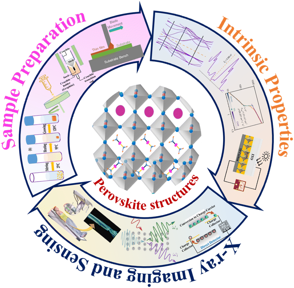
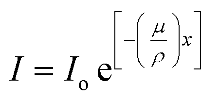
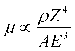


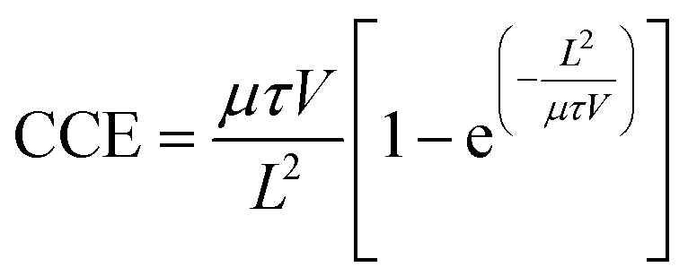


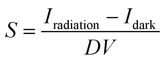
 . The thermal and shot noise are frequency independent and called white noise. Alternatively, the generation–recombination and flicker noise are frequency dependent.52 In addition, it has been reported that large resistivity can reduce the shot noise, and a large band gap leads to low thermal noise.53 Thus, a high resistance and large band gap are criteria for materials that can be used as a detector. The International Union of Pure and Applied Chemistry (IUPAC) declared that the detection limit of the producing signal value is three times the noise54 and the scientific community employs a signal-to-noise ratio (SNR) value of three to describe the limit of detection in radiation detection, especially X-ray detectors.55 The SNR is expressed by eqn (14).56
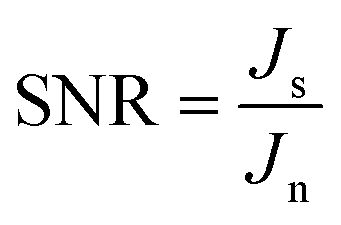
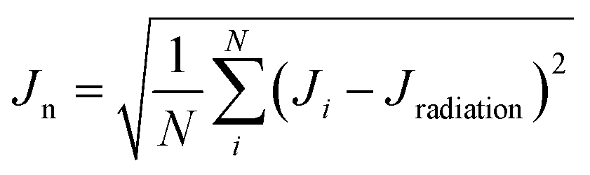
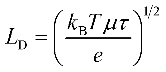
 (10–50 μm) is typically larger than that of electrons
  (1–5 μm).58 Thus, perovskite-based direct detectors function in hole collection mode. Generally, a longer diffusion length helps the carriers to accumulate at the respective electrode. In the case of radiation detectors, a longer LD is preferable because several millimeter-thick perovskite materials are used for completely absorbing high-energy radiation. Thus, the scientific community has attempted to increase LD by enhancing the bias voltage although it initiates the Idark, which hampers the device performance.59 In this case, by adopting a few modifications including structure design, optimized synthetic process and post-treatment, the μτ can be enhanced without initiating Idark. For an example, W. Pan and team increased the μτ from 3.75 × 10⁻³ cm2 V−1 to 6.3 × 10⁻³ cm2 V−1 for the SC structure of Cs2AgBiBr6 by adopting annealing post-treatment.60