 Open Access Article
Impact of selenization with NaCl treatment on the physical properties and solar cell performance of crack-free Cu(In,Ga)Se2 microcrystal absorbers†
Latha Marasamy *a,
Aruna-Devi Rasu Chettiar
 a,
Ravichandran Manisekaranb,
Evangeline Lindaa,
Md Ferdous Rahman
 c,
M. Khalid Hossain
 d,
Claudia Elena Pérez Garcíaa,
José Santos-Cruza,
Velumani Subramaniame and
Francisco de Moure Floresa
aFacultad de Química, Materiales-Energía, Universidad Autónoma de Querétaro (UAQ), Santiago de Querétaro, Querétaro C.P. 76010, Mexico. E-mail: latha.marasamy@uaq.mx
bInterdisciplinary Research Laboratory (LII), Nanostructures and Biomaterials Area, Escuela Nacional de Estudios Superiores Unidad León, Universidad Nacional Autónoma de México (UNAM), Predio el Saucillo y el Potrero, Comunidad de los Tepetates, León, C.P. 37684, Mexico
cDepartment of Electrical and Electronic Engineering, Advanced Energy Materials and Solar Cell Research Laboratory, Begum Rokeya University, Rangpur 5400, Bangladesh
dInstitute of Electronics, Atomic Energy Research Establishment, Bangladesh Atomic Energy Commission, Dhaka 1349, Bangladesh
eJ. Mike Walker '66 Department of Mechanical Engineering, Texas A&M University, Texas, 77843, USA
First published on 2nd February 2024
Abstract
In this study, we developed an ink using hexanethiol and Cu(In,Ga)Se2 microcrystals (CIGSe MCs) to make thin films via doctor blade coating. Besides, crack-free thin films were obtained by optimizing CIGSe MC powder concentration and annealing temperature. Subsequently, single-step selenization was performed with and without sodium chloride (NaCl) surface treatment by carefully tuning the temperature. A crack-free surface with densely packed grains was obtained at 500 °C after NaCl treatment. Moreover, the structural parameters of the thin film (annealed at 350 °C) were significantly modified via selenization with NaCl at 500 °C. For instance, the FWHM of the prominent (112) plane reduced from 1.44° to 0.47°, the dislocation density minimized from 13.10 to 1.40 × 10¹⁵ lines per m2, and the microstrain decreased from 4.14 to 1.35 × 10⁻³. Remarkably, these thin films exhibited a high mobility of 26.7 cm2 V−1 s−1 and a low resistivity of 0.03 Ω cm. As a proof of concept, solar cells were engineered with a device structure of SLG/Mo/CIGSe/CdS/i-ZnO/Al–ZnO/Ag, wherein a power conversion efficiency (PCE) of 5.74% was achieved with exceptional reproducibility. Consequently, the outcomes of this investigation revealed the impact of selenization temperature and NaCl treatment on the physical properties and PCE of hexanethiol-based crack-free CIGSe MC ink-coated absorbers, providing new insights into the groundwork of cost-effective solar cells.
1. Introduction
In thin-film photovoltaic technology, Cu-based chalcogenides, especially CIGSe semiconductors, have gained great interest owing to their direct and tunable bandgap, high optical absorption coefficient, long-term excitation stability, high quantum efficiency, and a PCE exceeding 23%.1 High PCE CIGSe solar cells have been fabricated using vacuum techniques such as co-evaporation and sputtering.1,2 However, vacuum techniques have persistent hurdles in commercializing CIGSe owing to complications in controlling its composition over a large area and high production costs.3,4 As an alternative, the solution process has attracted massive attention because of its cost-effectiveness, low material wastage, and applicability to large-scale deposition with controlled composition.5,6 One of the most promising approaches is the fabrication of low-cost solar cells via absorber layer coating using pre-synthesized quaternary CIGSe nanocrystal powder with a single-phase and targeted composition.7,8 Therefore, ink is commonly formulated by dispersing CIGSe nanocrystal powder in organic or inorganic solvents and subsequently coated as thin films onto a substrate via spin coating,9 blade coating,10 spray casting,11 drop-casting,7 and other methods.It is challenging to establish high-quality thin films such as crack-free dense layers using colloidal CIGSe nanocrystal ink as it develops cracks and voids during solvent evaporation. Typically, the nature of the solvent combined with ink formulation and coating conditions plays a vital role in realizing a crack-free uniform CIGSe nanocrystal layer. To date, the formulation of CIGSe nanocrystal inks has been demonstrated using tetrachloroethylene, hexane, dimethyl sulfoxide, and toluene.5,8,12,13 However, Guo et al. formulated sulfur-based CIGS nanocrystal ink using hexanethiol.6,10 However, information concerning the advancement of ink formation and coating conditions is scarce in the above-mentioned works. Harvey et al. recently reported a crack-free spray coating method for CIGSe nanocrystal ink using toluene, which helped attain uniform selenization.14 To our knowledge, no other reports are available on the elevation of CIGSe nanocrystal ink coatings using other solvents and coating processes, which provides numerous opportunities to explore them in detail.
In addition, the electrical conductivity of CIGSe nanocrystal-based thin films is constantly restricted due to the presence of residues from the solvents used during synthesis and ink formulation.15–17 Similarly, solar cell performance is firmly limited by nanosized grains.11,17–20 Therefore, CIGSe nanocrystal ink-coated thin films are subjected to high-temperature annealing under a Se/Ar atmosphere, known as the selenization process, to eliminate residues and obtain microsized grains. Several researchers have demonstrated enhancement in the selenization process by performing surface treatment (1 M NaCl), which leads to the formation of polyselenide phases that act as additional Se sources.6,10,14 Nonetheless, pre-selenization annealing for a long time (∼1 h), multiple ink coatings, and multistep selenization are required to obtain microsized grains, which are complex and time-consuming.14,19
Therefore, we were inspired to develop a facile single-step selenization process in the present work. In addition, we herein demonstrate the formulation of the ink using a CIGSe MC powder and a high-boiling point solvent of hexanethiol. The primary purpose of exploring the hexanethiol-based ink is to minimize the formation of cracks as it retains the nature of slow evaporation compared to low-boiling point solvents. As a result, we entrenched a crack-free coating by carefully optimizing the CIGSe MC powder concentration with the annealing temperature. Moreover, selenization temperature was carefully altered with and without NaCl treatment, and its impact on the physical properties of CIGSe was explored in detail. Consequently, crack-free thin films and densely packed grains were obtained after selenization. As a proof of concept, low-cost solar cells were fabricated with a PCE as high as 5.74%. Thus, the meaningful outcomes strongly reveal the establishment of a hexanethiol-based CIGSe MC ink-coated absorber and highlight its importance in enhancing the physical properties of CIGSe, which boosts solar cell performance.
2. Experimental details
2.1. Doctor blade coating of thin films using a CIGSe MC ink
First, a Cu0.9(In0.7Ga0.3)Se2 MC powder was synthesized following an experimental procedure similar to that reported in our previous work.17 Next, the ink was formulated by dispersing 100 mg of the synthesized CIGSe MC powder in 1000 μL of hexanethiol solvent, which was subsequently ultrasonicated at room temperature (RT) for 1 h. The soda-lime glass (SLG) substrates were cleaned in an ultrasonic bath with ethanol, acetone, and deionized water. Before doctor blade coating, the SLG substrate was dried under nitrogen gas. Then, an adhesive scotch tape was attached to the SLG substrate's two sides, acting as a spacer that offered uniform film coating and controlled thickness. Afterward, 15 μL of the formulated hexanethiol-based CIGSe MC ink was dropped onto one substrate edge, which was then swept around the substrate using a quartz glass rod (5 mm diameter) and left to dry naturally at RT. Subsequently, one more coating was applied in the opposite direction to obtain a uniform film with a thickness of ∼1 μm.The CIGSe MC powder concentrations of 100, 75, and 50 mg were tuned with a fixed hexanethiol volume of 1000 μL to obtain crack-free thin films. In addition, the as-coated thin films with different CIGSe MC powder concentrations were exposed to air annealing at 350 and 400 °C for 1 min. All the thin films were used for thickness measurements and morphological and compositional analyses.
2.2. Selenization of CIGSe MC thin films
A thin film prepared using 50 mg of CIGSe MC powder and annealed at 350 °C was chosen as the best and used further for the selenization process, as it showed a crack-free smooth surface. Therefore, the CIGSe MC thin film annealed at 350 °C was placed into a graphite box with 50 mg of elemental Se powder and then introduced into the furnace. Next, selenization was carried out under a Se/Ar atmosphere at 500 °C for 20 min at a heating ramp of 20 °C min−1. In addition, the selenization temperature was altered to 525 and 550 °C, while the selenization time was unchanged.Before the selenization process, NaCl treatment was performed by dipping the CIGSe MC thin film annealed at 350 °C into a 1 M solution. The selenization process was done at different temperatures, such as 500, 525, and 550 °C, for 20 min.
2.3. Characterization of CIGSe MC thin films
The morphologies of thin films (surface and cross-sectional images) were obtained using a field emission scanning electron microscope (FESEM; Auriga 3916, Carl Zeiss) operating at an accelerating voltage of 2 kV. An energy-dispersive X-ray spectrometer (EDS; XFlash Detector 5010) coupled with a FESEM was used to determine the elemental composition and mapping at 15 kV. The film thickness was determined using a profilometer (KLA Tencor P15). The crystal structure and phase were identified using an X-ray diffractometer (XRD; RIGAKU, Smart Lab) with Cu-Kα radiation (λ = 1.5406 Å) at 45 kV and 20 mA in the 2θ range from 20 to 60°. A Raman spectrometer (HORIBA Jobin Yvan) was used to confirm the crystal phase further using a He–Ne laser with a wavelength of 632 nm at RT. Optical absorption spectra were recorded at RT using an ultraviolet-visible-near infrared (UV-Vis-NIR; JASCO V-670) spectrophotometer. The electrical properties were measured at RT using a Hall-effect measurement system with a current of 0.1 mA accompanying a magnetic field strength of 0.51 T.2.4. Fabrication of CIGSe solar cells
CIGSe solar cells were fabricated with a substrate configuration of SLG/Mo/CIGSe/CdS/i-ZnO/Al–ZnO/Ag. The SLG substrates were cleaned using soap and deionized water in an ultrasonic bath. Before deposition of back contact, the SLG substrate was dried under nitrogen gas and loaded into a DC sputtering chamber. Next, the Mo layer (500 nm) was deposited onto SLG at 300 °C for 15 min with a sputtering power of 300 W and an Ar gas flow rate of 10 SCCM. After that, the absorber layer of CIGSe (∼1 μm) was deposited by the doctor blade coating method and was subsequently selenized with and without NaCl treatment following the same experimental procedure as mentioned in Sections 2.1 and 2.2. Later, a buffer layer of CdS (50 nm) was deposited by RF sputtering at RT for 20 min with a sputtering power of 25 W and an Ar gas flow rate of 10 SCCM. Afterward, the TCO layers of i-ZnO (40 nm) and Al–ZnO (100 nm) were deposited by RF sputtering at RT for 10 and 90 min, respectively, at a sputtering power of 50 W and an Ar gas flow rate of 5 SCCM. Finally, the solar cell fabrication was completed by depositing Ag contacts (50 nm) by thermal evaporation. The thickness of Mo, CdS, i-ZnO, and ZnO: Al layers was estimated by profilometry (KLA Tencor D-100). The current density vs. voltage (J–V) measurements were carried out using a solar simulator (LCS-100, Oriel instrument) calibrated at AM 1.5G.3. Results and discussions
3.1. Optimization of the CIGSe MC powder concentration to achieve crack-free thin films
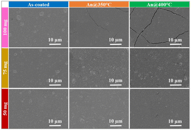
Attaining crack-free thin films by colloidal suspension coating is highly desirable for optoelectronic applications. Afterward, annealing of the as-coated thin films is essential to enhance the adherence of CIGSe onto the substrate and eliminate sulfur (S) that comes from the solvent (hexanethiol). Based on the abovementioned concerns, the CIGSe MC powder concentration was varied (100, 75, and 50 mg) at a fixed hexanethiol amount (1000 μL), coated as thin films, and annealed at different temperatures.Fig. 1 shows the FESEM images as a function of CIGSe MC powder concentration and annealing temperature. The as-coated thin films showed a smooth surface in all cases, whereas slight pin holes were detected at 100 mg. In addition, segregated crystals were noticed on the film surface with average sizes of 4, 3.5, and 2 μm for 100, 75, and 50 mg, respectively, which signifies a decrement in the crystal segregation by reducing the CIGSe MC powder concentration. Cracks were observed when the as-coated thin films with different CIGSe MC powder concentrations were annealed. As the annealing temperature was increased, crystal segregation weakened, whereas the cracks strengthened. However, the cracks drastically diminished as the CIGSe MC powder concentration decreased.
The coefficients of thermal expansion (CTE) of CIGSe and SLG substrates are 8–11 × 10−6 K−1 and 9 × 10⁻⁶ K−1, respectively.21 The observed cracks in the CIGSe MC thin film annealed at 350 °C (An@350 °C) could be due to the development of stress caused by the differences in the CTE of CIGSe and SLG. Cracks increased when the CIGSe MC thin film was annealed at 400 °C (An@400 °C), which could be related to the increased CTE difference at higher annealing temperatures.22–24 The observed cracks are also correlated with the volume shrinkage owing to the evaporation of S and carbon (C) contents, which creates stress, resulting in the development of cracks.25,26 The tendency of diminished cracks with reduced CIGSe MC powder concentration is strongly associated with a decreased film thickness, which lowers the CTE difference, as reported by other researchers.27 Among other conditions, a crack-free thin film was obtained using 50 mg CIGSe MC powder concentration and An@350 °C; therefore, this condition is considered the best and will be used for further selenization experiments.
Fig. 2 demonstrates the variations in the film thickness and S and C contents as a function of the CIGSe MC powder concentration and annealing temperature. The as-coated thin film showed thicknesses of 2.6, 2.1, and 1.45 μm for CIGSe MC powder concentrations of 100, 75, and 50 mg, respectively. As the CIGSe MC powder concentration decreased from 100 to 50 mg, the thickness reduced from 2.5 to 1.3 μm for CIGSe MCs thin film An@350 °C and it decreased further from 2.25 to 1.1 μm when the annealing temperature was raised to 400 °C. The trend of decreasing thin-film thickness is highly associated with the evaporation of S and C. The as-coated thin films exhibited S contents of 1, 2, and 3 (atomic%), and C contents of 47, 44, and 43 (atomic%) for CIGSe MC powder concentrations of 100, 75, and 50 mg, respectively. When the thin films were An@350 and 400 °C for all CIGSe MC powder concentrations, the S and C contents were reduced because of their evaporation compared to the as-coated thin film.
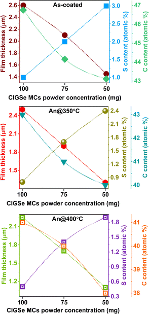 | ||
| Fig. 2 Changes in the film thickness and S and C contents as a function of CIGSe MC powder concentration and annealing temperature. | ||
Table S1† displays the EDS composition of thin films with regard to the CIGSe MC powder concentration and annealing temperature. From the table, the obtained elemental composition of Cu, In, Ga, and Se, and the ratio of Cu/In+Ga and Ga/In+Ga were very close to the CIGSe MC powder composition,17 which indicates the successful transformation of the CIGSe MC powder into thin films by means of developing a new hexanethiol-based ink.
3.2. Impact of selenization temperature with and without NaCl treatment on the physical properties of CIGSe MC thin films
Fig. 3 presents the planar and cross-sectional FESEM images of the CIGSe MC thin films selenized at diverse temperatures with and without NaCl. From the planar view, the CIGSe MC thin film An@350 °C showed a crack-free surface, as discussed in Section 3.1. A highly smooth crack-free surface was noticed when the CIGSe MC thin film was selenized at 500 °C (Se@500 °C) with and without NaCl, validating that selenization improves the quality of the thin films. However, cracks appeared when the selenization temperature increased to 525 °C (Se@525 °C), which intensified at 550 °C (Se@550 °C), correlating with the increase in the CTE differences between SLG and CIGSe by raising the selenization temperature,22–24 A similar behavior was also noticed in the NaCl-treated thin films. Nevertheless, Se@525 and Se@550 °C with NaCl demonstrated fewer cracks and randomly distributed grains with a size of ∼1 μm on the thin-film surface than NaCl-free thin films.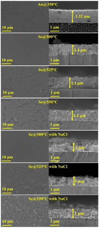 | ||
| Fig. 3 FESEM images of the CIGSe MCs thin films selenized at different temperatures with and without NaCl. | ||
From the cross-sectional view, the thin-film An@350 °C showed a thickness of 1.32 μm, which was reduced to 1.1 μm after selenization associated with the evaporation of S and C, as shown in Table 1 and grain boundary reduction. The thickness remained unchanged as the selenization temperature increased from 500 to 550 °C. In the case of NaCl-treated thin films, the thickness decreased to 1 μm, which correlated with enhancement in the grain packing density by reducing the grain boundaries. Crystallization was improved by increasing the selenization temperature in both cases (with and without NaCl). Nonetheless, it is interesting to note that NaCl-treated samples revealed significant enrichment in crystallization, concurrent with the efficient selenization process. For instance, during selenization, elemental Se from Se vapors reacts with Na present on the thin-film surface; thus, Na2Sex (polyselenide) phases are formed, acting as additional Se sources.28–30 Besides, the polyselenide phases reacted rapidly with metal cations from CIGSe, facilitating crystallization and grain growth. Therefore, enhancement in the quality of CIGSe MC thin films with NaCl-treated thin films is highly linked to the creation of polyselenide phases that behave as catalysts by supplying more Se to CIGSe than Na-free samples.31
| Samples name | Composition (atomic%) | Cu/(In+Ga) | Ga/(In+Ga) | S (atomic%) | Na (atomic%) | C (atomic%) | |||
|---|---|---|---|---|---|---|---|---|---|
| Cu | In | Ga | Se | ||||||
| An@350 °C | 23.15 | 17.96 | 7.80 | 51.09 | 0.90 | 0.30 | 1.88 | 0.34 | 41.90 |
| Se@500 °C | 22.91 | 17.84 | 7.72 | 51.53 | 0.90 | 0.30 | — | 1.62 | 25.02 |
| Se@525 °C | 23.21 | 17.16 | 7.28 | 52.35 | 0.95 | 0.30 | — | 1.65 | 25.26 |
| Se@550 °C | 23.66 | 16.87 | 7.32 | 52.15 | 0.98 | 0.30 | — | 1.65 | 25.10 |
| Se@500 °C with NaCl | 22.95 | 18.02 | 7.58 | 51.45 | 0.90 | 0.30 | — | 5.10 | 25.51 |
| Se@525 °C with NaCl | 23.11 | 17.14 | 7.46 | 52.29 | 0.94 | 0.30 | — | 5.10 | 25.20 |
| Se@550 °C with NaCl | 23.80 | 16.82 | 7.35 | 52.03 | 0.98 | 0.30 | — | 5.08 | 25.11 |
Based on the morphological analysis, the samples of An@350 °C, Se@500 °C and Se@500 °C with NaCl thin films exhibited a crack-free surface. Therefore, we selected these samples to study the thickness distribution. In Fig. S1,† we present the FESEM images taken at both low and high magnifications. The low-magnification images (Fig. S1a–c†) demonstrate uniform thicknesses of 1.32, 1.1 and 1 μm for An@350 °C, Se@500 °C and Se@500 °C with NaCl thin films, respectively. Meanwhile, the high-magnification images (Fig. S1d–f†) display eighteen points, which were used to plot the thickness distribution. Fig. S1g–i† shows that all samples have a narrow thickness distribution ranging from 1.32 to 1.36 μm, 1.1 to 1.18 μm, and 1 to 1.04 μm for An@350 °C, Se@500 °C, and Se@500 °C with NaCl thin films, respectively. This indicates that the thin films have a high level of uniformity.
From Table 1, the observed ratios of Cu/In+Ga and Ga/In+Ga from Se@500 °C were analogous to those of the reference sample (An@350 °C). However, when the selenization temperature was increased above 500 °C, the Cu/In+Ga ratio increased slightly, whereas the Ga/In+Ga ratio was unaffected. This tendency was also observed for NaCl-treated thin films. The slight increment in the Cu/In+Ga ratio could be associated with the high mobility of Cu at high temperatures.32
The CIGSe MC thin film An@350 °C revealed S and Na contents of 1.88 and 0.34 (atomic%), respectively. After selenization, S disappeared because of its volatile nature, whereas Na increased to ∼1.6 (atomic%) due to its diffusion from the SLG substrate. A high Na content of ∼5 (atomic%) was obtained for NaCl-treated thin films, which is obviously due to the external Na provided during treatment in addition to the SLG substrate. The observed C value of ∼41.9 (atomic%) from the An@350 °C thin film is derived from the organic solvents oleylamine and hexanethiol, which were utilized to synthesize CIGSe MC powder17 and ink formulation, respectively. Interestingly, C drastically decreased from 41.9% to ∼25% after selenization due to its decomposition at higher temperatures. It has been challenging to eliminate the C content because it is firmly bonded to the CIGSe MC surface; however, it has not been inevitably detrimental to the solar cell performance,33,34 and a detailed investigation regarding the impact of C content is yet to be explored.
FESEM-EDS mapping was performed for the MC thin film Se@500 °C with NaCl, as depicted in Fig. 4, to observe the elemental distributions of Na, Cu, In, Ga, and Se. The elemental mapping was performed in the area marked in dark red color, as indicated in Fig. 4a. The Na, Cu, In, Ga, and Se contents were uniformly distributed throughout the marked area, as shown in Fig. 4b–f, which strongly proves the homogeneous distribution of these elements. The obtained composition of Cu![[thin space (1/6-em)]](https://www.rsc.org/images/entities/char_2009.gif) :
:![[thin space (1/6-em)]](https://www.rsc.org/images/entities/char_2009.gif) In
In![[thin space (1/6-em)]](https://www.rsc.org/images/entities/char_2009.gif) :
:![[thin space (1/6-em)]](https://www.rsc.org/images/entities/char_2009.gif) Ga
Ga![[thin space (1/6-em)]](https://www.rsc.org/images/entities/char_2009.gif) :
:![[thin space (1/6-em)]](https://www.rsc.org/images/entities/char_2009.gif) Se was found to be 0.90
Se was found to be 0.90![[thin space (1/6-em)]](https://www.rsc.org/images/entities/char_2009.gif) :
:![[thin space (1/6-em)]](https://www.rsc.org/images/entities/char_2009.gif) 0.30
0.30![[thin space (1/6-em)]](https://www.rsc.org/images/entities/char_2009.gif) :
:![[thin space (1/6-em)]](https://www.rsc.org/images/entities/char_2009.gif) 0.70
0.70![[thin space (1/6-em)]](https://www.rsc.org/images/entities/char_2009.gif) :
:![[thin space (1/6-em)]](https://www.rsc.org/images/entities/char_2009.gif) 2, whereas a Na content of ∼5 (atomic%) was observed as displayed in Fig. 4g, which is consistent with the results presented in Table 1.
2, whereas a Na content of ∼5 (atomic%) was observed as displayed in Fig. 4g, which is consistent with the results presented in Table 1.
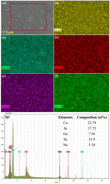 | ||
| Fig. 4 (a) FESEM image, (b–f) EDS mapping, and (g) EDS spectrum of the CIGSe MCs thin film Se@500 °C with NaCl. | ||
Fig. 5 represents the Raman spectra of the CIGSe MC thin films selenized at diverse temperatures with and without NaCl. From the figure, a peak was detected at 174 cm−1 for all cases, which aligns well with the prominent A1 mode of CIGSe, representing the vibration of metal cations of Cu, In, and Ga, while Se is at rest.35 The A1 mode peak position remained unaffected with regard to the Na content, as reported by other researchers.36–38 The absence of other Raman peaks confirms the presence of single-phase CIGSe. The full width at half maximum (FWHM) was calculated for all samples shown in Fig. 5.
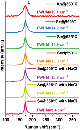 | ||
| Fig. 5 Raman spectra of CIGSe MC thin films selenized at different temperatures with and without NaCl. | ||
Remarkably, the CIGSe MC thin film Se@500 °C with and without NaCl exhibited a massive change in the FWHM explicitly difference of 4.9 and 6.8 cm−1 respectively, concerning An@350 °C, denoted the significant improvement in the crystallinity of CIGSe after selenization. However, differences in the FWHM of 5.8 (without NaCl) and 9.7 cm−1 (with NaCl) were perceived when the selenization temperature was raised to 550 °C. From these results, it can be inferred that NaCl treatment tremendously boosts the selenization process as NaCl-treated samples demonstrated a more significant variation in the FWHM than NaCl-free, resulting in enhanced crystallinity, indicating the quality of CIGSe was greatly amplified.
Fig. 6 displays the XRD patterns of the CIGSe MCs thin films selenized at different temperatures with and without NaCl. The peaks observed at 26.87, 44.62, and 53.93° are consistent with the chalcopyrite crystal structure of (112), (220), and (312) planes for all cases (JCPDS 35-1102). No significant peak shift was observed for different selenization temperatures with and without NaCl, which indicates that the CIGSe peak position is independent of the Na content, as reported in the literature.39–41 The FWHM was determined for a prominent peak matching the (112) plane. The CIGSe MC thin film An@350 °C showed an FWHM of 1.44°, whereas Se@500 °C with and without NaCl treatment demonstrated 0.65° and 0.47° respectively, revealing an enormous enhancement in the crystallinity of selenized CIGSe thin films, as it showed a FWHM difference of 0.79 and 0.97° concerning An@350 °C. When the selenization temperature increased to 550 °C, the FWHM difference of 0.82° (without NaCl) and 1.08° (with NaCl) was noticed with respect to An@350 °C. These results strongly confirm that NaCl treatment strengthens the crystallinity of CIGSe MC thin films compared to NaCl-free samples.
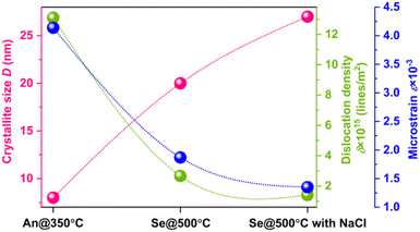 | ||
| Fig. 6 XRD patterns of the CIGSe MC thin films selenized at different temperatures with and without NaCl. | ||
Based on the morphological results, the best CIGSe MC thin films, namely An@350 °C and Se@500 °C with and without NaCl, were selected to investigate the structural parameters and optical and electrical properties, as they displayed crack-free surfaces.
The structural parameters such as crystallite size (D), dislocation density (δ), and strain (ε) were calculated and are shown in Fig. 7. The crystallite size (D) was determined for the prominent (112) plane using Debye Scherrer's formula:42
 | (1) |
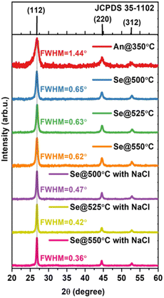 | ||
| Fig. 7 Changes in the structural parameters as a function of CIGSe MCs thin film An@350 °C and Se@500 °C with and without NaCl. | ||
Dislocation density (δ) signifies the number of defects existing in the CIGSe crystals and was calculated using the following formula:43
 | (2) |
Microstrain was estimated using the following formula:44
 | (3) |
The CIGSe MC thin films An@350 °C and Se@500 °C without and with NaCl exhibited D values of 8, 20, and 27 nm, respectively, revealing a massive improvement in crystallinity, especially after selenization, wherein the NaCl-treated thin film demonstrated the highest D value.38 The δ values of CIGSe MC thin films An@350 °C and Se@500 °C without and with NaCl were 13.10, 2.66, and 1.40 × 10¹⁵ lines per m2 respectively. Indeed, Se@500 °C without and with NaCl thin films demonstrated a drastic reduction in δ, specifically 4.92 and 9.36 times, respectively, compared to An@350 °C. Additionally, the NaCl-treated sample demonstrated a significant decrease in δ, i.e., 1.9 times that of the NaCl-free sample. The An@350 °C showed ε of 4.14, whereas Se@500 °C without and with NaCl indicated that 1.87 and 1.35, respectively, signified a lowered ε due to increased D. Consequently, the attained significant findings strongly indicate an extensive improvement in the structural parameters, which could significantly influence the electrical and optoelectronic properties of CIGSe.
Fig. 8a exhibits the UV-Vis-NIR absorbance spectra of the CIGSe MC thin films An@350 °C and Se@500 °C with and without NaCl. All the CIGSe MC thin films showed a similar behavior; absorption originated in the NIR region, which gradually expanded towards the UV-Vis region. No considerable shift in the UV-Vis region was detected because of the similar elemental compositions of Cu, In, Ga, and Se. Fig. 8b shows the estimation of the bandgap energy by extrapolating hν versus (αhν)2 using the Tauc relation. The obtained bandgap energy values from 1.30 to 1.32 eV are in the optimum range, which is in agreement with other reports.17,45 No significant change in the bandgap energy again proved a similar CIGSe composition. Besides, these results imply that the optical properties of CIGSe thin films are unrelated to the Na content, as reported in the literature.31,46
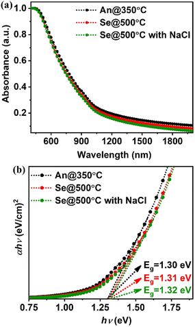 | ||
| Fig. 8 (a) UV-Vis-NIR absorbance spectra and (b) corresponding bandgap of hν versus (αhν)2 of CIGSe MC thin films An@350 °C and Se@500 °C with and without NaCl. | ||
Table 2 illustrates the electrical properties of CIGSe MC thin films concerning An@350 °C and Se@500 °C with and without NaCl. From the table, p-type conductivity was observed in all cases. The carrier concentration vastly enhanced from 2.4 × 10¹⁶ (An@350 °C) to 1.2 × 10¹⁷ (Se@500 °C with NaCl), which is highly associated with the Na content present in the CIGSe MC thin films.38,46
| Thin films | Conductivity type | Carrier concentration (cm−3) | Resistivity (Ω cm) | Mobility (cm2 V−1 s−1) | Ref. | |
|---|---|---|---|---|---|---|
| Cu(In0.75Ga0.25)Se2 | P | 1.95 × 10¹⁸ | 2.41 | 2.92 | 8 | |
| Cu(In0.70Ga0.30)Se2 | P | 2 × 10¹⁷ | 2.03 | 3.24 | 7 | |
| Cu(In0.70Ga0.30)Se2 | P | 2 × 10¹⁷ | 0.37 | 11.92 | 32 | |
| Cu0.90(In0.70Ga0.30)Se2 | P | 2.3 × 10¹⁶ | 0.44 | 11.46 | 17 | |
| Cu0.97(In0.70Ga0.30)Se2 | P | 2.5 × 10¹⁷ | 0.31 | 12.04 | ||
| Cu0.90(In0.70Ga0.30)Se2 | An@350 °C | P | 2.4 × 10¹⁶ | 0.42 | 11.50 | Present work |
| Se@500 °C | P | 9.9 × 10¹⁶ | 0.11 | 18.2 | ||
| Se@500 °C with NaCl | P | 1.2 × 10¹⁷ | 0.03 | 26.7 | ||
As mentioned earlier (Table 1), the CIGSe MC thin films An@350 °C and Se@500 °C without and with NaCl showed Na contents of 0.34, 1.62, and 5.10 (atomic%), respectively. Therefore, the formation of NaIn and NaCu defects is strongly favorable; however, NaCu is electrically static, whereas NaIn significantly increases the carrier concentration. Usually, a Cu-poor CIGSe sample (Cu/In+Ga < 1) unveils the formation of InCu defects, which are then converted into NaCu when Na is introduced into the Cu-poor CIGSe MCs thin films. Thus, a high number of NaCu is generated during the selenization process at a higher temperature, which is thermodynamically unstable when it cools down after selenization. As a result, Na is prone to out-diffuse from the CIGSe grain interior, which leads to the creation of VCu, consequently increasing the carrier concentration.46,47 This effect usually occurs in the solution-based Na incorporation approaches such as dissolving NaCl in water and ammonia-based solutions, wherein Na dissolves on the surface of CIGSe MC thin films, thereby lowering the chemical potential of Na, leading to more robust outward diffusion of Na from the grain interior of CIGSe. The CIGSe MC thin films An@350 °C and Se@500 °C without and with NaCl demonstrated mobilities of 11.50, 18.2, and 26.7 cm2 V−1 s−1, whereas resistivities of 0.42, 0.11, and 0.03 Ω cm respectively. The photogenerated charge carriers commonly reach contact when the light-absorbing semiconductor maintains fewer crystal defects and less strain along with better crystallinity; as a result, mobility enriches and resistivity drops. Therefore, the observed tendency of increased mobility and decreased resistivity in this work is firmly correlated with enhanced crystallinity, grain size, and reduced dislocation density and microstrain as a function of CIGSe thin films An@350 °C and Se@500 °C with and without NaCl. Besides, the attained carrier concentration in the order of 1016 and 1017 cm−3 is in the optimum range for solar cell applications.17,32 Furthermore, it is worth highlighting that the present work demonstrates higher mobility and lower resistivity among other reports available by a solution process from the literature, as detailed in Table 2.
3.3. Effect of selenization with and without NaCl treatment on the CIGSe solar cell performance
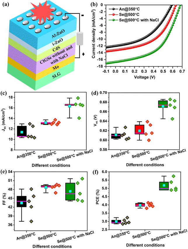
The CIGSe MC thin films demonstrated a profound change in their morphological, structural, and electrical properties as a function of An@350 °C and Se@500 °C with and without NaCl. Hence, it is considerably energizing to fabricate thin-film solar cells by incorporating CIGSe MC-based absorbers.The CIGSe solar cells were fabricated with a substrate device configuration, as shown in Fig. 9a. The J–V measurements were performed under AM 1.5G illumination with an intensity of 100 mW cm−2 and a total contact area of 0.24 cm2. Fig. 9b shows the best J–V curves among the five different CIGSe solar cells under each condition. The obtained open-circuit voltage (Voc), short-circuit current density (Jsc), as well as estimated fill factor (FF), and power conversion efficiency (PCE) are shown in Table 3. The CIGSe MC thin films An@350 °C and Se@500 °C without and with NaCl revealed Voc of 0.61, 0.64, and 0.69 V; Jsc of 12.51, 13.23, and 16.68 mA cm−2; FF of 42, 49, and 50%; PCE of 3.23, 4.13, and 5.74% respectively. This outcome strongly validates the significant enhancement in the solar cell parameters when the CIGSe MC thin film An@350 °C was subjected to Se@500 °C with and without NaCl. This behavior is highly associated with changes in the intrinsic properties of CIGSe with regard to the Na content, which modifies the solar cell performance. For instance, the Na content enhanced the following properties: carrier concentration increased by creating a higher number of VCu; crystallinity improved by reducing dislocation density and microstrain; grain compactness enhanced along with the increase in grain size. Consequently, the mobility was boosted by 2.32 times, and the resistivity was decreased by 14 times, supposedly responsible for the reduced recombination rate of photogenerated charge carriers. Therefore, the consequential research output decisively concludes that the inclusion of Na substantially improved the morphological, structural, and electrical properties of the CIGSe absorber.
| Different conditions | Voc (V) | Jsc (mA cm−2) | FF (%) | PCE (%) | |
|---|---|---|---|---|---|
| An@350 °C | Best average | 0.613 | 12.51 | 42.12 | 3.23 |
| 0.611 ± 0.010 | 11.38 ± 1.25 | 43.43 ± 4.13 | 3 ± 0.15 | ||
| Se@500 °C | Best average | 0.639 | 13.23 | 48.85 | 4.13 |
| 0.620 ± 0.016 | 13.18 ± 0.35 | 48.74 ± 1.09 | 3.98 ± 0.13 | ||
| Se@500 °C with NaCl | Best average | 0.686 | 16.68 | 50.16 | 5.74 |
| 0.671 ± 0.016 | 16.35 ± 1.39 | 47.38 ± 3.41 | 5.18 ± 0.37 | ||
As a result, the PCE of solar cells enriched by 1.3 and 1.8 times corresponds to the CIGSe thin films Se@500 °C without and with NaCl, respectively, compared with An@350 °C.
To ensure the reliability of data and reproducibility of the solar cells' performance, five CIGSe solar cells were fabricated under each condition. The statistical distributions of solar cell parameters such as Voc (V), Jsc (mA cm−2), FF (%), and PCE (%) are presented in Fig. 9c–f. The average values and standard deviation are listed in Table 3. Comprehensive information on the performance of each solar cell is given in the ESI (Table S2†). From the table and Fig. 9c–f, a minimal standard deviation was noticed, especially in the case of PCE, indicating the high reproducibility of the solar cell performance.
Table 4 compares the solar cell performance obtained from ternary (CuInSe2) and quaternary (CuInGaSe2) nanocrystal ink-coated absorbers. From the table, it is apparent that Jsc (mA cm−2), Voc (V), FF (%), and PCE (%) of the solar cells were significantly altered as a function of CIGSe composition and device configuration. However, there are obstacles in the ternary and quaternary-based nanocrystal ink approaches, namely, hurdles in accomplishing densely packed grains with smooth surfaces and achieving microsized grains. Therefore, we are urged to look for solutions such as searching for a new solvent in which dense thin films together with crack-free surfaces can be accomplished and developing MC ink. In this concern, we established a new approach in which thin films were prepared from the hexanethiol-based CIGSe MC ink. In addition, a detailed investigation was conducted, wherein the CIGSe MC powder concentration and selenization temperature with and without NaCl were optimized. Consequently, we achieved a PCE as high as 5.74%, which is 1.12 times higher than the maximum PCE reported in the literature.18 Moreover, these results are highly reproducible and reliable, as previously stated. Furthermore, thin films were prepared by a doctor blade coating, which has several advantages such as high suitability for large-scale deposition, easy control of thickness, and less material wastage, among other methods. Consequently, the meaningful outcomes of this work highlight the importance of accomplishing crack-free thin films by hexanethiol-based CIGSe MC ink coating and the impact of selenization temperature with and without NaCl on the physical properties and solar cell performance of CIGSe.
| Nanocrystal absorber and coating method | Solar cell configuration | Jsc (mA cm−2) | Voc (V) | FF (%) | PCE (%) | Ref. |
|---|---|---|---|---|---|---|
| CuInSe2 by drop casting | SLG/Mo/CuInSe2/CdS/i-ZnO/ITO | 3.20 | 0.30 | 25.0 | 0.24 | 5 |
| CuInSe2 by drop casting | SLG/Mo/CuInSe2/CdS/i-ZnO/ITO/Ag | 25.8 | 0.28 | 39.0 | 2.82 | 48 |
| CuIn0.75Ga0.25Se2 by spray coating | Glass/Au/CuInGaSe2/CdS/i-ZnO/ITO/Ag | 3.50 | 0.38 | 41.0 | 0.51 | 49 |
| CuInSe2 by spray coating | SLG/Cr/Au/CuInSe2/CdS/ZnO/ITO | 16.3 | 0.41 | 46.0 | 3.10 | 50 |
| CuInSe2 by spray coating | Glass/Mo/CuInSe2/CdS/ZnO/ITO | 6.40 | 0.38 | 48.5 | 1.18 | 51 |
| Glass/Au/CuInSe2/CdS/ZnO/ITO | 8.30 | 0.48 | 48.8 | 1.93 | ||
| Cu0.82In0.68Ga0.25Se2 by spin coating | SLG/Mo/CuInGaSe2/CdS/i-ZnO/Al–ZnO/Ag | 17.33 | 0.30 | 49.7 | 2.62 | 52 |
| CuInSe2 by spray coating | SLG/Au/CuInSe2/CdS/ZnO/ITO | 1.85 | 0.18 | 29.7 | 0.1 | 53 |
| CuInSe2 by spray coating | SLG/Cr/Au/CuInSe2-oleylamine/CdS/i-ZnO/ITO/Ag | 9.59 | 0.35 | 46.7 | 1.56 | 54 |
| SLG/Cr/Au/CuInSe2-MCC/CdS/i-ZnO/ITO/Ag | 10.96 | 0.34 | 45.0 | 1.68 | ||
| CuIn0.85Ga0.15Se2 | SLG/Mo/CuInGaSe2/CdS/ZnO/ITO/Ag | 8.50 | 0.24 | 34.0 | 0.69 | 18 |
| CuIn0.75Ga0.25Se2 | SLG/Mo/CuInGaSe2/CdS/ZnO/ITO/Ag | 13.59 | 0.32 | 36.0 | 1.56 | |
| CuIn0.50Ga0.50Se2 | SLG/Mo/CuInGaSe2/CdS/ZnO/ITO/Ag | 20.10 | 0.53 | 48.0 | 5.10 | |
| CuIn0.25Ga0.75Se2 | SLG/Mo/CuInGaSe2/CdS/ZnO/ITO/Ag | 9.08 | 0.48 | 35.0 | 1.51 | |
| CuGaSe2 (all samples by spray coating) | SLG/Mo/CuGaSe2/CdS/ZnO/ITO/Ag | 1.81 | 0.20 | 28.0 | 0.10 | |
| CuIn0.61Ga0.39Se2 by spray coating | SLG/Cr/Au/CuInGaSe2/CdS/i-ZnO/ITO/Ag | 5.26 | 0.25 | 31.7 | 0.42 | 55 |
| CuIn0.7Ga0.3Se2 by spray coating | Mo/CuInGaSe2/CdS/i-ZnO/Al–ZnO/SLG | 8.0 | 0.46 | 30.0 | 1.11 | 11 |
| Cu0.90In0.70Ga0.30Se2 by drop casting | Mo/CuInGaSe2-MCs/CdS/ZnO/Al:ZnO/Ag | 9.54 | 0.69 | 51.32 | 3.38 | 17 |
| Cu0.90In0.70Ga0.30Se2 by doctor-blade coating | Mo/CuInGaSe2-MCs/CdS/ZnO/Al:ZnO/Ag | 16.68 | 0.67 | 50.16 | 5.74 | Present work |
4. Conclusions
We have successfully developed a new ink based on hexanethiol and CIGSe MCs, wherein crack-free coating was established by carefully varying the CIGSe MC powder concentrations such as 100, 75, and 50 mg in 1000 μL hexanethiol and annealing temperature. Furthermore, one-step selenization was performed with and without NaCl treatment. Moreover, the selenization temperature was adjusted to 500, 525, and 550 °C at a fixed time of 20 min. The CIGSe thin film Se@500 °C with NaCl exhibited compact grains and crack-free surfaces. Besides, the structural property of thin film An@350 °C was greatly influenced after selenization at 500 °C with NaCl, explicitly the FWHM of A1 mode peak from Raman analysis significantly reduced from 19.1 to 12.3 cm−1, while the FWHM of the (112) plane from XRD decreased from 1.44 to 0.47°. Moreover, the electrical resistivity decreased from 0.42 to 0.03 Ω cm, whereas the mobility enhanced from 11.50 to 26.7 (cm2 V−1 s−1), and the carrier concentration increased by one order of magnitude from 1016 to 1017 (cm−3) after selenization at 500 °C with NaCl. As a validation, cost-effective solar cells were fabricated with a PCE as high as 5.74%. The reproducibility of solar cells' performance was explored, wherein a very low standard deviation was noticed, signifying the very high reproducibility of low-cost solar cells. Therefore, we strongly believe that this work demonstrates the establishment of new ink and the importance of selenization with and without NaCl on the physical properties and solar cell performance of a hexanethiol-based CIGSe MC ink-coated absorber.Conflicts of interest
There are no conflicts to declare.Acknowledgements
The authors would like to acknowledge the partial financial support from “Fondo Química Somos Todos-UAQ-2021” to carry out this work.References
- M. Nakamura, K. Yamaguchi, Y. Kimoto, Y. Yasaki, T. Kato and H. Sugimoto, IEEE J. Photovoltaics, 2019, 9, 1863–1867 Search PubMed.
- P. Jackson, R. Wuerz, D. Hariskos, E. Lotter, W. Witte and M. Powalla, Phys. Status Solidi RRL, 2016, 10, 583–586 CrossRef CAS.
- H. R. Hsu, S. C. Hsu and Y. S. Liu, Sol. Energy, 2012, 86, 48–52 CrossRef CAS.
- M. Powalla and B. Dimmler, Thin Solid Films, 2000, 361, 540–546 CrossRef.
- M. G. Panthani, V. Akhavan, B. Goodfellow, J. P. Schmidtke, L. Dunn, A. Dodabalapur, P. F. Barbara and B. A. Korgel, J. Am. Chem. Soc., 2008, 130, 16770–16777 CrossRef CAS PubMed.
- S. M. McLeod, C. J. Hages, N. J. Carter and R. Agrawal, Prog. Photovoltaics Res. Appl., 2015, 23, 1550–1556 CrossRef CAS.
- M. Latha, R. Aruna-Devi, S. Velumani, J. Santoyo-Salazar and F. de Moure-Flores, Adv. Powder Technol., 2019, 30, 2980–2988 CrossRef CAS.
- M. Latha, R. Aruna Devi and S. Velumani, Opt. Mater., 2018, 79, 450–456 CrossRef CAS.
- T. T. T. Le, N. Le, M. R. Pallavolu, Y. Jeon, D. seob Jeong, B. Pejjai, V. R. M. Reddy, N. T. N. Truong and C. Park, Korean J. Chem. Eng., 2019, 36, 2110–2117 CrossRef CAS.
- Q. Guo, G. M. Ford, R. Agrawal and H. W. Hillhouse, Prog. Photovoltaics Res. Appl., 2013, 21, 64–71 CrossRef CAS.
- A. C. Badgujar, R. O. Dusane and S. R. Dhage, Sol. Energy, 2020, 199, 47–54 CrossRef CAS.
- R. G. Ellis, J. W. Turnley, D. J. Rokke, J. P. Fields, E. H. Alruqobah, S. D. Deshmukh, K. Kisslinger and R. Agrawal, Chem. Mater., 2020, 32, 5091–5103 CrossRef CAS.
- J. Tang, S. Hinds, S. O. Kelley and E. H. Sargent, Chem. Mater., 2008, 20, 6906–6910 CrossRef CAS.
- T. B. Harvey, F. Bonafé, T. Updegrave, V. R. Voggu, C. Thomas, S. C. Kamarajugadda, C. J. Stolle, D. Pernik, J. Du and B. A. Korgel, ACS Appl. Energy Mater., 2019, 2, 736–742 CrossRef CAS.
- X. Zhang, S. Liu, F. Wu, X. Peng, B. Yang and Y. Xiang, Nanoscale Res. Lett., 2018, 13, 1–7 CrossRef PubMed.
- D. Zhao, Y. Wu, B. Tu, G. Xing, H. Li and Z. He, Nanomaterials, 2019, 9, 286 CrossRef CAS PubMed.
- L. Marasamy, A. D. Rasu Chettiar, F. de Moure-Flores and V. Subramaniam, Int. J. Energy Res., 2021, 45, 6966–6984 CrossRef CAS.
- V. A. Akhavan, T. B. Harvey, C. J. Stolle, D. P. Ostrowski, M. S. Glaz, B. W. Goodfellow, M. G. Panthani, D. K. Reid, D. A. Vandenbout and B. A. Korgel, ChemSusChem, 2013, 6, 481–486 CrossRef CAS PubMed.
- T. B. Harvey, I. Mori, C. J. Stolle, T. D. Bogart, D. P. Ostrowski, M. S. Glaz, J. Du, D. R. Pernik, V. A. Akhavan, H. Kesrouani, D. A. Vanden Bout and B. A. Korgel, ACS Appl. Mater. Interfaces, 2013, 5, 9134–9140 CrossRef CAS PubMed.
- O. A. Ali and B. A. Korgel, Eng. & Tech. J., 2015, 33, 1753–1760 Search PubMed.
- F. Kessler and D. Rudmann, Sol. Energy, 2004, 77, 685–695 CrossRef CAS.
- P. De Lima-Neto, A. N. Correia, G. L. Vaz and P. N. S. Casciano, J. Braz. Chem. Soc., 1968, 21, 1968–1976 CrossRef.
- P. De Lima-Neto, A. N. Correia and G. P. Da Silva, J. Braz. Chem. Soc., 2006, 17, 1419–1427 CrossRef CAS.
- E.-H. A. Mohamed, Mater. Sci. Appl., 2011, 02, 439–443 CAS.
- C. Liewhiran and S. Phanichphantandast, Sensors, 2007, 7, 650–675 CrossRef CAS.
- P. Xu, A. S. Mujumdar and B. Yu, Drying Technol., 2009, 27, 636–652 CrossRef.
- W. Fang and C.-Y. Lo, Sens. Actuators, A, 2000, 84, 310–314 CrossRef CAS.
- D. Braungera, D. Hariskosa, G. Bilgerb, U. Raub and H. W. Schock, Thin Solid Films, 2000, 361, 161–166 CrossRef.
- O. Nwakanma, S. Velumani and A. Morales-Acevedo, Mater. Today Energy, 2021, 20, 100617 CrossRef CAS.
- F. Hergert, S. Jost, R. Hock, M. Purwins and J. Palm, Thin Solid Films, 2007, 515, 5843–5847 CrossRef CAS.
- S. Uličná, L. M. Welch, A. Abbas, M. Togay, V. Tsai, T. R. Betts, A. V. Malkov, J. M. Walls and J. W. Bowers, Prog. Photovoltaics Res. Appl., 2021, 29, 546–557 CrossRef.
- M. Latha, R. Aruna-Devi, S. Velumani, B. Murali, J. Santoyo-Salazar and F. De Moure-Flores, RSC Adv., 2019, 9, 35197–35208 RSC.
- V. Haug, A. Quintilla, I. Klugius and E. Ahlswede, Thin Solid Films, 2011, 519, 7464–7467 CrossRef CAS.
- A. Cho, S. Ahn, J. H. Yun, Y. J. Eo, H. Song and K. Yoon, Sol. Energy Mater. Sol. Cells, 2013, 110, 126–132 CrossRef CAS.
- A. Chirila, S. Seyrling, S. Buecheler, D. Guettler, S. Nishiwaki, Y. E. Romanyuk, G. Bilger and A. N. Tiwari, Prog. Photovoltaics Res. Appl., 2012, 20, 209–216 CrossRef CAS.
- Y. M. Shin, D. H. Shin, J. H. Kim and B. T. Ahn, Curr. Appl. Phys., 2011, 11, S59–S64 CrossRef.
- M. Wang, M. A. Hossain and K. L. Choy, Sci. Rep., 2017, 7, 6788 CrossRef PubMed.
- B. J. Babu, S. Velumani, B. J. Simonds, R. K. Ahrenkiel, A. Kassiba and R. Asomoza, Mater. Sci. Semicond. Process., 2015, 37, 37–45 CrossRef CAS.
- W. Li, X. Yan, A. G. Aberle and S. Venkataraj, Sci. Rep., 2019, 9, 2637 CrossRef PubMed.
- G. Rajan, B. Belfore, S. Karki, D. Poudel, H. Kahoui, N. Lanham, E. Palmiotti, S. Soltanmohammad, A. Rockett and S. Marsillac, Thin Solid Films, 2019, 690, 137526 CrossRef CAS.
- S. Ye, X. Tan, M. Jiang, B. Fan, K. Tang and S. Zhuang, Appl. Opt., 2010, 49, 1662–1665 CrossRef CAS PubMed.
- S. Saber, B. Marí, A. Andrio, J. Escorihuela, N. Khattab, A. Eid, A. El Nahrawy, M. A. Aly and V. Compañ, Nanomaterials, 2021, 11, 1093 CrossRef CAS PubMed.
- P. K. Mishra, V. Dave, J. N. Prasad, A. K. Choudhary and R. Chandra, Procedia Technol., 2014, 14, 219–227 CrossRef.
- H. Saïdi, C. Ben Alaya, M. F. Boujmil, B. Durand, J. L. Lazzari and M. Bouaïcha, Curr. Appl. Phys., 2020, 20, 29–36 CrossRef.
- W. Li, S. Xu, Y. Dai, P. Ma, Y. Feng, W. Li, H. Luo and C. Yang, Mater. Lett., 2019, 244, 43–46 CrossRef CAS.
- A. C. Badgujar, R. O. Dusane and S. R. Dhage, Sol. Energy, 2020, 209, 1–10 CrossRef CAS.
- Z. K. Yuan, S. Chen, Y. Xie, J. S. Park, H. Xiang, X. G. Gong and S. H. Wei, Adv. Energy Mater., 2016, 6, 1601191 CrossRef.
- Q. Guo, S. J. Kim, M. Kar, W. N. Shafarman, R. W. Birkmire, E. A. Stach, R. Agrawal and H. W. Hillhouse, Nano Lett., 2008, 8, 2982–2987 CrossRef CAS PubMed.
- D. P. Ostrowski, M. S. Glaz, B. W. Goodfellow, V. A. Akhavan, M. G. Panthani, B. A. Korgel and D. A. Vanden Bout, Small, 2010, 6, 2832–2836 CrossRef CAS PubMed.
- V. A. Akhavan, M. G. Panthani, B. W. Goodfellow, D. K. Reid and B. A. Korgel, Opt. Express, 2010, 18, A411–A420 CrossRef CAS PubMed.
- V. A. Akhavan, B. W. Goodfellow, M. G. Panthani, D. K. Reid, D. J. Hellebusch, T. Adachi and B. A. Korgel, Energy Environ. Sci., 2010, 3, 1600–1606 RSC.
- J. H. Lee, J. Chang, J. H. Cha, Y. Lee, J. E. Han, D. Y. Jung, E. C. Choi and B. Hong, Eur. J. Inorg. Chem., 2011, 647–651 CrossRef CAS.
- C. Steinhagen, V. A. Akhavan, B. W. Goodfellow, M. G. Panthani, J. T. Harris, V. C. Holmberg and B. A. Korgel, ACS Appl. Mater. Interfaces, 2011, 3, 1781–1785 CrossRef CAS PubMed.
- C. Stolle Jackson, M. G. Panthani, T. B. Harvey, V. A. Akhavan and B. A. Korgel, ACS Appl. Mater. Interfaces, 2012, 4, 2757–2761 CrossRef CAS PubMed.
- G. Jia, K. Wang, B. Liu, P. Yang, J. Liu, W. Zhang, R. Li, C. Wang, S. Zhang and J. Du, RSC Adv., 2019, 9, 35780–35785 RSC.
Footnote |
| † Electronic supplementary information (ESI) available: EDS composition of thin film with respect to CIGSe MCs powder concentration along with annealing temperature, comprehensive solar cell parameters, FESEM images of An@350 °C, Se@500 °C and Se@500 °C with NaCl thin films at low and high magnifications and (g–i) corresponding thickness distribution. See DOI: https://doi.org/10.1039/d3ra05829h |
| This journal is © The Royal Society of Chemistry 2024 |

