 Open Access Article
Creative Commons Attribution 3.0 Unported Licence
Two-dimensional materials for photoelectrochemical water splitting
Sang Eon
Jun†
 a,
Jae Kwan
Lee†
a and
Ho Won
Jang
 *ab
*ab
aDepartment of Materials Science and Engineering, Research Institute of Advanced Materials, Seoul National University, Seoul 08826, Korea. E-mail: hwjang@snu.ac.kr
bAdvanced Institute of Convergence Technology, Seoul National University, Suwon, 16229, Republic of Korea
First published on 27th October 2022
Abstract
Two-dimensional (2D) materials have sparked in-depth research in various fields due to their entirely distinct electronic and mechanical properties compared to their bulk counterpart. In a photoelectrochemical cell, 2D materials can serve crucial roles by incorporating their unique and extraordinary characteristics into semiconducting photoabsorbers to boost the unassisted solar water splitting. To this end, this review summarizes the intrinsic superiorities of 2D materials derived using van der Waals interactions between individual layers and presents the utilization of 2D materials to improve the photoelectrochemical performance of photoelectrodes. In addition, the emerging state-of-the-art 2D materials, including transition metal dichalcogenides (TMDs), graphene, graphdiyne, black phosphorus (BP), layered double hydroxides (LDHs), g-C3N4, and MXenes, will be introduced. Delicately constructed heterostructures with photoabsorbers and 2D materials are capable of highly efficient light harvesting for both hydrogen and oxygen evolution. Finally, critical outlooks on developing synthetic technology for mass production, improving stability issues, and constructing tandem architectures for unbiased solar water splitting will be discussed.
1. Introduction
Environmental pollution and the energy crisis on the earth are two of the most serious issues that must be addressed. To this end, renewable energy, including solar and wind energy, have tremendous potential to alleviate the present sense of crisis due to its abundance.1 Especially, the amount of solar energy radiated on the earth in 1 hour is similar to all of the energy consumed on the earth in a year.2 To convert sunlight into useful electricity, various types of photovoltaic cells have been invented and they are now being operated in our daily life. However, high variability and intermittency of sunlight illumination could degrade the stability of the electrical grid when an enormous amount of electricity is generated instantly.3 In addition, it is difficult to transmit intensively produced electricity from one area to another area where the electrical grid is not connected. As a result, it is necessary to construct an energy storage system suitable for stable production, distribution, and utilization.4–6 Compared to electricity, hydrogen can be stored independently without any network and it is easy to transport by land and sea for worldwide distribution.7,8 Furthermore, it is expected to become sustainable future energy due to its non-toxicity, zero-emission, and large energy density.9 It can be obtained by an electrochemical approach integrated with solar harvesting systems such as photovoltaic–electrochemical (PV–EC) and photoelectrochemical (PEC) water splitting.10–12 In the PV–EC system, the electricity generated from a photovoltaic cell is supplied to an electrochemical water electrolyzer and converts H2O into H2 and O2 while the photogenerated charges participate in hydrogen and oxygen evolution reaction at the surface of photoelectrodes in the PEC system.13 Compared to PEC, the advantage of PV–EC is that the matured technologies are developed in both solar cells and water electrolyzers. Also, the solar-to-hydrogen efficiency of PV–EC is higher than that of PEC until now. However, for practical solar hydrogen production exhibiting both high efficiency and low system complexity, it is necessary to develop PEC cells with efficiency greater than 10% and stability of more than 10 years.14 To meet these criteria, various types of semiconducting materials have been investigated for photoelectrochemical light harvesting.13–15 For photocathodes where photo-induced hydrogen evolution reaction (HER) occurs, p-type semiconductors such as p-Si,16 Cu2O,17 Sb2Se3,18 and CIGS19 have been widely studied. In the case of photoanodes in which photo-assisted oxygen evolution reaction (OER) occurs, n-type semiconductors including n-Si,20–23 TiO2,24–26 WO3,27 BiVO4,28,29 and α-Fe2O330 have been reported. Although these materials have the potential to be utilized as photoelectrodes for unassisted solar water splitting,31 there are still limitations to obtaining enough solar-to-hydrogen (STH) efficiency and stability to fulfill cost-effective hydrogen production.32,33 It is derived from various factors such as insufficient output photovoltage, catalytic inactivity, light reflection on the surface, and photo/chemical-induced corrosion of photoelectrodes.12,34,35 Hence, it is crucial that the photoelectrodes be assisted by the PEC catalysts. Also, the appropriate atomic-scale designs including engineering of defect, heteroatom, facet, phase, and single atoms are needed for both the photoelectrodes and catalysts to facilitate the photogenerated charge transfer and surface catalytic reaction.36Two-dimensional (2D) materials have been extensively investigated for PEC catalysts with exceptional properties which could replace noble metals (Pt, IrOx, and RuOx).37,38 They have recently emerged as promising materials in energy harvesting, storage, and conversion because of their large specific surface area,39 stackability for heterostructure construction,40 surface functionalization,41 and thickness-dependent optoelectronic properties.42 With these properties, they serve crucial roles as active PEC catalysts, interfacial transporting layers, passivation layers, and light harvesters for both HER and OER. Specifically, 2D materials with edge sites, defects, phase transformation, ion-exchanged sites, and synergistic composites can dramatically lower the free energy required for the surface reaction. Also, they become the charge transport mediators by being junctioned (Schottky junction, p–n junction, and multi-heterojunction) with semiconducting photoelectrodes. In addition, the surface of photoelectrodes vulnerable to the electrolyte is protected by electrochemically stable 2D materials and it leads to long-term stability. 2D materials having band gap even can be used for photon harvesters and their PEC performance can be improved by surface treatments and heterostructures.
In this review, we focus on 2D materials and their properties to acquire a significantly efficient and stable photoelectrode. Fig. 1 shows the representative 2D materials and their roles in photoelectrochemical water splitting. Firstly, the unique characteristics and superiorities of 2D materials will be introduced. Secondly, we review how 2D materials have been utilized for PEC water splitting and their roles in active catalysts, interfacial transporting layers, passivation layers, and light harvesters. Thirdly, the state-of-the-art 2D materials including transition metal dichalcogenides (TMDs), noble metal dichalcogenides, graphene, graphdiyne, black phosphorus (BP), layered double hydroxide (LDHs), g-C3N4, and MXenes will be introduced. Finally, several insights regarding the synthetic approach for mass production, stability issues derived from the desorption of 2D materials, and tandem devices for unassisted solar water splitting will be discussed with a perspective on future challenges and suggest solutions to enhance the photoelectrochemical performance.
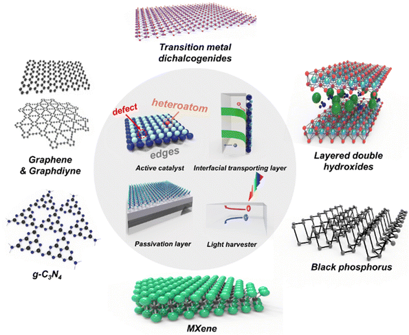 | ||
| Fig. 1 Schematic illustrations of 2D materials and their roles in photoelectrochemical water splitting. | ||
2. Superiority of 2D materials
The layers of 2D materials interact with each other via weak van der Waals force, while strong covalent bonds exist within the plane.43,44 Using weak interlayer interactions, it is possible to exfoliate 2D materials into monolayers or nanosheets. These interactions, the most remarkable characteristic of 2D materials, provide the unique superiorities that a material with 0D, 1D, and 3D network structure can not possess such as large specific surface area,45 stackability for heterostructure,37 bandgap tuning,46 and surface functionalization.472.1. Large specific surface area
The large lateral size with ultrathin thickness enables 2D materials to have a high specific surface area. It allows the maximized active planes and atoms to be exposed. Hence, 2D materials are versatile for surface-active applications, including energy conversions, batteries, supercapacitors, gas sensors, etc. in which the reactants interact at the surface. For energy conversion applications such as HER, OER, and CO2RR, a large number of active sites where the reacting elements (H+, OH−, and CO2) participate in the reaction are provided.48 The larger the specific surface area, the more efficiently the reactants are consumed, and a larger amount of desired resultants are obtained. For various types of batteries using Li+, Na+, and Zn+ as transporting ions, the improved ion absorption and transportation are achieved by large surface area and shortened transfer path, respectively, leading to high energy density and rate capability.49 In terms of gas sensing applications, a large surface area of 2D materials provides numerous active sites for gas adsorption resulting in a strong improvement in the sensitivity of the sensor.502.2. Stackability for heterostructure
The van der Waals interactions enable 2D materials to be stacked into arbitrary substrates or layers without crystal mismatch and atomic interdiffusion, while conventional covalently bonded materials mechanically affect adjacent layers.37 Especially, atomic scale high-quality heterostructures are realized by stacking different 2D materials on top of each other.44 The most intriguing aspect is that high-quality Schottky junctions, p–n junctions, and multi-heterojunctions are achieved without intrinsic surface states within the energy band gap of 2D materials. It reduces the possibility of charge recombination, achieving a longer lifetime of charges going through the heterointerface. In addition, the local electron density of 2D heterostructures can be redistributed via van der Waals forces, leading to unpaired orbital electrons derived from a change in electron configuration.51 This phenomenon induces easier molecule adsorption and desorption, boosting the surface catalytic reaction. For these reasons, they provide flexibility to be utilized with lots of van der Waals heterostructure combinations (0D–2D, 1D–2D, 2D–2D, and 3D–2D).52 These combined dimensionality offer possibilities in various applications including energy conversions and storages,53,54 optoelectronics,55 sensors,56 and field-effect transistors.572.3. Tunable band gap
The energy band gap implies the minimum energy demanded to excite an electron from the valence energy band (ground state) into the conduction energy band.58 In van der Waals layered structures, the band gap can be controlled by the number of layers due to the electron confinement along horizontal sheets and the energy splitting of band edges derived from the interlayer hopping.59 There are several 2D materials having adjustable energy band gaps ranging from the mid-infrared in BP, visible in TMDs, to the ultraviolet in h-BN. Not only the thickness, many studies have revealed that the band gaps of 2D materials can be tuned by heterostructuring,60 strain engineering,61 intercalations,62 chemical doping,63 and alloying.64 For instance, when a large strain is applied to the graphene, the inversion symmetry of the crystal lattice is broken, enabling it to open a bandgap in its gapless band structure.65,66 Also, Mo1−xWxS2 monolayer, one of the TMD alloys, shows the band gap bowing depending on W composition.67 It is attributed to the unequal contribution of metal elements to the lowest unoccupied molecular orbital (LUMO) of the alloy, resulting in the occurrence of LUMO bowing. These thickness, mechanical, and composition-dependent band gap emission of 2D materials play crucial roles in devices requiring optimal band alignment such as field effect transistors, light-emitting diodes, and photoelectrodes/photocatalysts.2.4. Surface functionalization
The pristine state of 2D materials has a certain degree of innate active sites such as edges and defects. However, by enlarging these active sites or introducing foreign impurities on the surface, unique mechanical, electrical, magnetic, and electrochemical properties can be obtained. In particular, chemical doping and anchoring functional units onto 2D materials induce novel properties improving dispersibility, wettability, processability, and environmental stability.47 There are two types of 2D material functionalization depending on the way of interactions, which are non-covalent and covalent conjugation. The non-covalent method controls the electronic and physical properties without distorting crystal structures and physically adsorbed elements cause an effect via van der Waals or electrostatic forces.68 On the other hand, covalent modification induces the rehybridization of orbitals by constructing covalent chemical building blocks between 2D materials and reactive molecules.69 Both of them utilize molecular building blocks which can ultimately change the electronic characteristics of 2D materials via charge transfer or dipole-dipole interactions.703. Utilization of 2D materials in PEC water splitting
3.1. Active catalysts
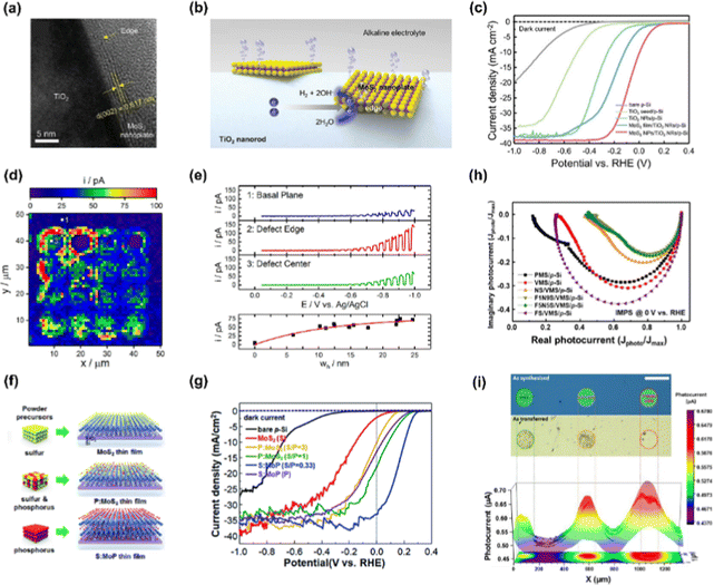
In a photoelectrochemical water splitting system, one of the most crucial roles of 2D materials is boosting the catalytic reaction at the surface by lowering Gibbs free energy of ion adsorption and gas desorption. Despite the high activity of noble metal catalysts (Pt, IrOx, and RuOx), low-cost 2D materials have the potential to surpass precious metal catalysts via proper engineering. 2D materials intrinsically have catalytic active sites such as edges and defects. However, it is necessary to augment and expose them as much as possible to achieve vigorous photoelectrolysis.71,72 Lots of studies have revealed that exceptionally active edges and defects can be induced by strain engineering,73 plasma treatment,74 foreign elements doping,75 and so on. Li et al. theoretically predicted and verified that elaborately strained and electrochemically generated sulfur vacancies in the basal plane of monolayer MoS2 serve as highly active sites for hydrogen evolution reaction.76,77 Moreover, the highly active photoelectrochemical catalysts can be acquired by deliberately inducing phase transformation, exchanging anion or cation of 2D materials, and combining them with other materials exhibiting a synergistic effect.3.2. Interfacial transporting layers
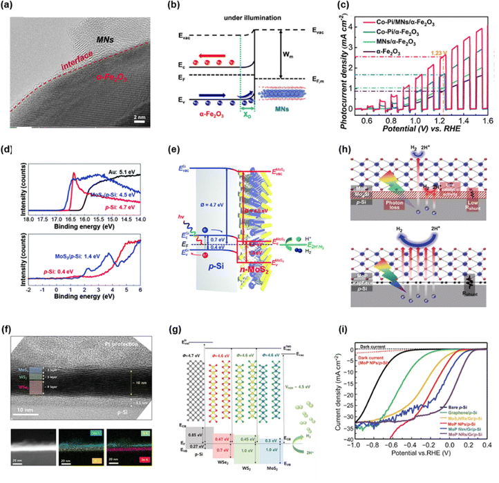
The photo-induced charge carriers generated from semiconductors tend to make recombination before arriving at the surface of photoelectrodes. To achieve highly efficient charge flow from the semiconductor to the electrolyte, it is necessary to construct interfacial transporting layers. The 2D materials, which can easily be adjusted in thickness and constructed anywhere, are suitable for interfacial transporting layers. The electronic properties including band gap and work function can be acquired by analyzing X-ray photoelectron spectroscopy (XPS) and ultraviolet photoelectron spectroscopy (UPS). Using these data, energy band diagram regarding the junction of semiconducting photoabsorber and 2D material can be demonstrated. If the Schottky junction, p–n junction, and multi-heterojunction are established at the interface, the photogenerated charges can easily transfer by the electric field derived from energy band bending. In addition, 2D materials are capable of inhibiting the formation of secondary compounds between photoelectrode and catalyst. As the interfacial secondary compound hinders the charge transport, it is necessary to prevent them by using 2D materials that can be stacked into substrates without crystal mismatch and atomic interdiffusion.3.3. Passivation layers
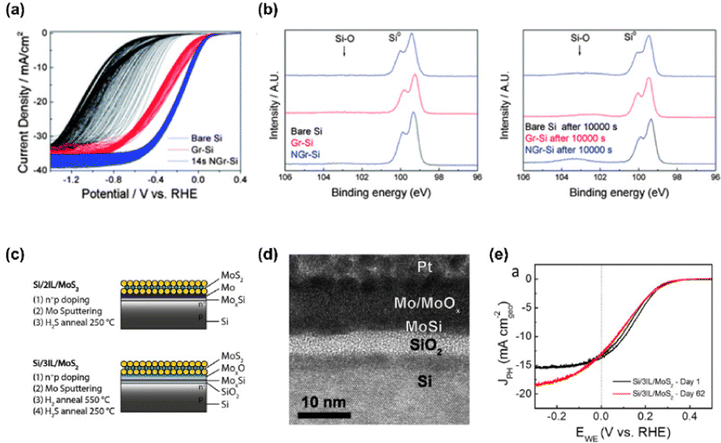
Sim et al. introduced plasma-treated N-doped monolayer graphene on p-Si photocathode as both a PEC catalyst and a passivation layer.98 To synthesize N-doped graphene, N2-plasma with 10 W power was treated for 14 s. The passivation effect of graphene and N-doped graphene was investigated by 300 cycles of cyclic voltammetry (CV) in Fig. 4(a). As the CV cycle increased, bare Si showed a large negative shift. However, the silicon photocathodes with graphene and N-doped graphene exhibited only shifts in the onset potential of 0.1 and 0.035 V, respectively. In Fig. 4(b), XPS spectra of the Si 2p region for each sample before and after the stability test for 10![[thin space (1/6-em)]](https://www.rsc.org/images/entities/char_2009.gif) 000 s were provided to reveal the capability of graphene to passivate the silicon surface. In the case of graphene and N-doped graphene on silicon, only a small increase in the Si–O peak was observed while the peak of bare Si increased a lot after the stability test. It indicates that graphene suppresses the oxidation of the silicon surface during photoelectrochemical hydrogen production.
000 s were provided to reveal the capability of graphene to passivate the silicon surface. In the case of graphene and N-doped graphene on silicon, only a small increase in the Si–O peak was observed while the peak of bare Si increased a lot after the stability test. It indicates that graphene suppresses the oxidation of the silicon surface during photoelectrochemical hydrogen production.
King et al. demonstrated a stable silicon photocathode with a protecting layer that is composed of 2D molybdenum disulfide, molybdenum silicide, and silicon oxide.99 In Fig. 4(c), the schematics of the MoS2 catalyst and additional protection layers on the silicon photocathode are presented. They suggested two systems. One has two interlayers (MoxSi and Mo) and the other has three interlayers (SiO2, MoxSi, and MoOx). Fig. 4(d) shows the cross-sectional TEM image of a photocathode with three interlayers (MoOx/MoSix/SiO2) and it is concluded that the overall thickness of MoS2 with three interlayers is greater than that of MoS2 with two interlayers due to a thicker MoOx and SiO2. In Fig. 4(e), cyclic voltammograms of photocathode with three interlayers on both day 1 and day 62 showed an excellent onset potential of 0.31 V vs. RHE and photocurrent density, which proved the passivation effect of MoS2 and three interlayers.
3.4. Light harvesters
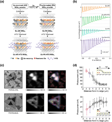
Yu et al. investigated the role of defects on the PEC performance of 2D WSe2 thin film photocathodes by applying two different treatments, a pre-exfoliation annealing and a post-deposition surfactant attachment to eliminate intraflake and edge defects, respectively.100 The schematics of WSe2 flake with treatments and the resulting atomic structures were provided in Fig. 5(a). After pre-exfoliation annealing, few internal Se vacancies exist at the lattice of WSe2. In addition, the exposed edge vacancies were filled by surfactant after the treatment with hexyl-trichlorosilane. As can be seen in Fig. 5(b), the WSe2 photocathode with both pre-exfoliation annealing and surfactant attachment showed the highest photocurrent density (4.0 mA cm−2) at 0 V vs. RHE among the samples (Exfoliation with as-received WSe2, HTS treatment after exfoliation with as-received WSe2, exfoliation with pre-annealed WSe2, and HTS treatment after exfoliation with pre-annealed WSe2). While only the pre-annealing did not affect the performance, upon applying both the pre-annealing and HTS treatment, an enhanced PEC performance was identified.Wang et al. analyzed charge recombination and transport pathways as a function of stacking configuration in MoS2/WS2 junction photoelectrode.101 They performed the image analysis procedure to investigate parallel charge transport pathways. In Fig. 5(c), the optical transmission images and photocurrent maps of ITO/MoS2/WS2 and ITO/WS2/MoS2 are provided. The bright contrast pixels of MoS2/WS2 extended beyond the heterojunction boundary while the dark contrast pixels of WS2/MoS2 occur deeper within the heterojunction interior. To quantitatively analyze how the heterojunction influenced parallel charge transport, the photocurrent value versus distance between WS2 and the nearest heterojunction edge site was obtained in Fig. 5(d). In the case of WS2 on MoS2, the photocurrent increased monotonically with decreasing d and showed a maximized value inside the heterojunction region. However, for the stacking configuration with WS2 under MoS2, the photocurrent decreased with decreasing d.
4. State-of-the-art 2D materials for PEC water splitting
4.1. Transition metal dichalcogenides (TMDs)
TMDs are one of the most promising materials for PEC applications due to their unique optical, electrical, and catalytic properties. In particular, the edges and defects serve as good active sites, exhibiting excellent photoelectrochemical catalytic performance. Recently, various transition metal-based dichalcogenides consisting of MoS2,102 WS2,103 WSe2,96 NbS2,104 PtSe2,105 and ReSe2106 have been developed for solar water splitting with strategies such as edge engineering, morphology control, thickness control, and heterostructuring.W-based TMDs also exhibit considerable photoelectrochemical catalytic properties. Hasani et al. conducted the direct synthesis of WS2 on p-Si via the thermolysis process.108 The surface of the silicon wafer has become hydrophilic by depositing the WO3 layer as a pretreatment and (NH4)WS4 precursor was coated on a hydrophilic substrate with good adhesion. Then, the as-fabricated (NH4)WS4/WO3/p-Si was converted to WS2/p-Si by simple thermolysis at 900 °C. The thickness-optimized (38 nm) WS2/p-Si photocathode showed great PEC performance with a photocurrent density of −9.8 mA cm−2 at 0 V vs. RHE and an onset potential of 0.022 V vs. RHE. In addition, the WS2/p-Si photocathode showed good stability with no decrease in current density even after 40 h.
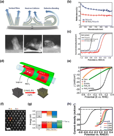
NbS2 is a representative metallic TMDs having a highly active basal plane for hydrogen adsorption and desorption, as can be identified by its near-zero hydrogen adsorption Gibbs free energy.109 Gnanasekar et al. demonstrated an efficient and stable Si nanowires photocathode by depositing NbS2 using a CVD method.104Fig. 6(d) shows the schematic image of NbS2 growth on Si NWs using a CVD method. The LSV curves of the fabricated photocathodes are shown in Fig. 6(e) and NbS2/Si NWs shows an onset potential of 0.34 V vs. RHE and photocurrent density of −28 mA cm−2 at 0 V vs. RHE.
4.2. Carbon allotropes
4.3. Black phosphorus (BP)
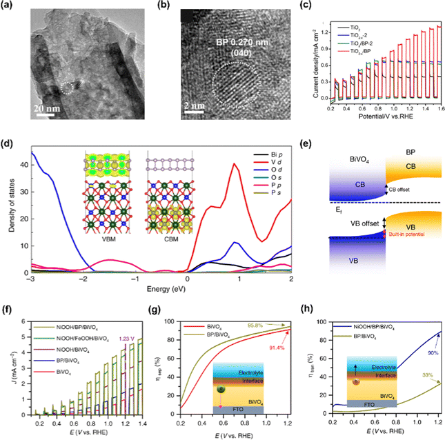
Black phosphorus, one of the allotropes of phosphorus, is a thermodynamically stable layered semiconductor having a narrow band gap that can be obtained from white or red phosphorus at high pressure and temperature due to a phase transition.127 To date, pressure-induced atomic structural change of 2D material has only been identified in black phosphorus as orthorhombic atomic structure changes to rhombohedral and cubic at 5 and 10 GPa, respectively. The high carrier mobility of black phosphorus and tunable energy band gap from 0.3 to 2.0 eV enables them to become a promising material in various electronic and energy conversion applications.Zheng et al. firstly constructed a TiO2−x/BP heterojunction photoanode with the strategies of black phosphorus quantum dots (BPQDs) sensitization and oxygen vacancies introduction to TiO2 nanotube arrays (NTAs).128 The BPQDs were prepared by dispersing BP crystals in NMP and sonicating them for several hours. The BPQDs were spin-coated onto the TiO2 NTAs in which the oxygen vacancies were created after being soaked in NaBH4 solution. In Fig. 8(a) and (b), TEM images of TiO2−x/BP photoanode were provided and the distinct lattice fringes of 0.270 nm correspond to the (040) planes of BP, indicating that BPQDs have been successfully synthesized. The synergistic effect of the synthesized BPQDs and oxygen vacancies induced NTAs enhances the PEC performance by improving charge separation and increasing active sites. Fig. 8(c) shows the LSV curve of the TiO2−x/BP electrode and it produced a photocurrent density of 1.12 mA cm−2 at 1.23 V vs. RHE, which is more than three times that of pristine TiO2.
Zhang et al. verified that the intrinsic p-type black phosphorus contributes to the hole extraction from BiVO4 photoanode and prolongs the trapping lifetime of charges on the BiVO4 surface by characterizing OEC/BP/BiVO4.129 In Fig. 8(d), the density of states (DOS) of BP/BiVO4 heterojunction was provided and it was confirmed that BP nanosheets change the valence band of BiVO4via the overlap of the P 2p and O 2p orbitals without affecting the conduction band minimum of BiVO4. The band offset and built-in potential of the BP/BiVO4 heterojunction are demonstrated in Fig. 8(e). Under external bias, the positrons serving as the dominant carriers across the BP/BiVO4 heterointerface promote hole extraction from BiVO4 to BP. As shown in Fig. 8(f), an obvious increase in photocurrent density derived from the insertion of BP was observed. The NiOOH/BP/BiVO4 photoanode achieved a photocurrent density of 4.48 mA cm−2 at 1.23 V vs. RHE, which is 1.5 times higher than that of the NiOOH/BiVO4 photoanode. Furthermore, the insertion of BP also improved the charge separation efficiency of BiVO4 as can be seen in Fig. 8(g). The enhanced charge separation efficiency clearly proved the role of BP as an efficient hole extraction material. In addition, the introduction of the NiOOH catalyst on BP/BiVO4 boosted the charge transfer efficiency, enabling highly efficient water oxidation at the surface.
4.4. Layered double hydroxides (LDHs)
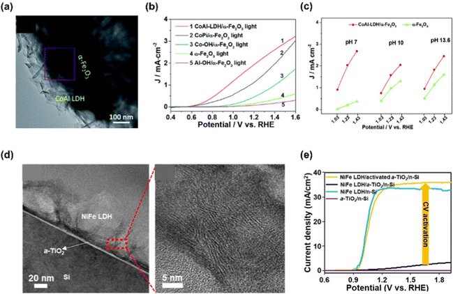
LDHs are a type of anionic clay having a layered structure defined as a unique atomic formula of [M1−x2+Mx3+ (OH)2](An−)x/n·mH2O. M2+ and M3+ are divalent and trivalent metal cations, and An− is a charge-balancing anion.130 Mg, Fe, Co, Cu, Ni, Zn are used as M2+, and Al, Cr, Ga, Mn are used as M3+. Commonly, LDHs consist of layers of metal cations having similar ionic radii, which are coordinated by six oxygen atoms with the structure of M2+/M3+(OH)6 octahedra.131 These octahedra construct two-dimensional sheet by sharing edges and the sheets are stacked together via hydrogen bonding between the hydroxyl groups.Chong et al. demonstrated a highly efficient and stable α-Fe2O3 photoanode in neutral pH condition by decorating CoAl-LDH via the hydrothermal method.132 In Fig. 9(a), the TEM image shows the successful synthesis of CoAl-LDH and compact integration of LDH with α-Fe2O3. In Fig. 9(b), the LSV curves of α-Fe2O3, CoAl-LDH/α-Fe2O3, Co–OH/α-Fe2O3, Al–OH/α-Fe2O3, and CoPi/α-Fe2O3 were provided. Compared to bare α-Fe2O3, the CoAl-LDH/α-Fe2O3 exhibited drastically improved PEC water oxidation in neutral pH electrolyte as the onset potential was shifted to cathodic direction by 250 mV and the photocurrent density was increased 9-fold at 1.23 V vs. RHE. The authors explained that Co provided active sites for water oxidation while Al provided the support for the layered skeleton. In addition, the layered structure assisted H2O to access the Co active sites. Not only in neutral pH electrolyte but also in high pH media, CoAl-LDH/α-Fe2O3 shows superior PEC-OER performance at various applied potentials as can be seen in Fig. 9(c).
Choi et al. fabricated a Si photoanode with remarkable PEC performance using cyclic voltammetry (CV)-activated amorphous TiO2 and NiFe LDH.133 Amorphous TiO2 interlayer was synthesized via ALD method followed by CV activation in 1 M NaOH solution with the applied potential from −1 to 1 V vs. Ag/AgCl. After this procedure, NiFe LDH thin film catalyst was synthesized by electrodeposition. In Fig. 9(d), the TEM image of NiFe LDH/activated α-TiO2/n-Si and the HR-TEM image of NiFe LDHs were presented. The hierarchical porous structure of NiFe LDH was compactly formed on α-TiO2/n-Si substrate and it is beneficial to the smooth release of the product and the diffusion of ions. The PEC-OER performance of the fabricated NiFe LDH/activated 5 nm α-TiO2/n-Si photoanode is shown in Fig. 9(e). For the photoanode without TiO2 activation, poor performance was shown due to a large band gap, facile charge recombination, and low charge transfer of the TiO2 layer. After CV activation of TiO2, the photoanode showed superior J–V characteristics due to oxygen vacancies facilitating hole transfer. The synergistic heterostructure exhibited an onset potential of 0.92 ± 0.1 V vs. RHE and a photocurrent density of 36 mA cm−2 at 1.23 V vs. RHE.
4.5. Graphitic carbon nitride (g-C3N4)
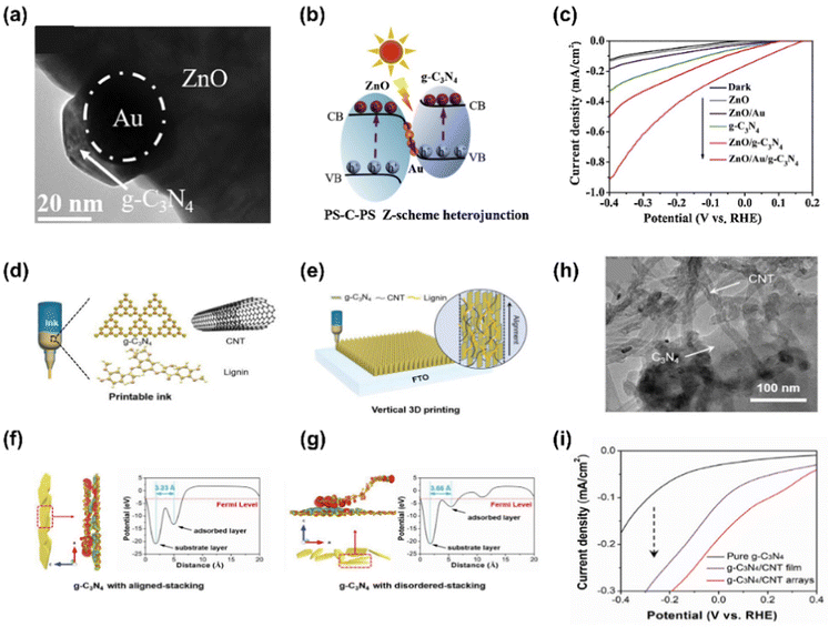
Graphitic carbon nitride (g-C3N4) is considered an attractive material in photoelectrochemistry and photocatalysis due to its excellent visible light reactivity, suitable band gap, physicochemical stability, low cost, and pollution-free feature.134 However, there are some restrictions to be improved such as insufficient solar light absorption, low surface area, and fast charge recombination. To date, various strategies to obtain high-performance g-C3N4 have been conducted by elemental doping, morphology control, enlarging porosity, and heterostructuring.135,136Wen et al. fabricated an all-solid-state 3D urchin-like ZnO/Au/g-C3N4 heterojunction photocathode showing a highly efficient PEC hydrogen evolution.137 For the fabrication of the photocathode, ZnO seeds were grown into 3D urchin-like ZnO nanorods by hydrothermal method and Au was deposited by ultrasonication of ZnO nanorods with HAuCl4 precursor. Then, g-C3N4 was synthesized by thermal vapor condensation (TVC) in melamine III followed by coating on the FTO substrate by drop casting. In Fig. 10(a), the TEM image shows that Au nanoparticles are well attached to urchin-like ZnO and g-C3N4 surrounds the Au NPs compactly. The schematic in Fig. 10(b) shows the charge transfer mechanism of ZnO/Au/g-C3N4 ternary heterojunction under light illumination. In this mechanism, Au NPs with high work function (−5.30 eV) act as mediators promoting electron transfer from ZnO to g-C3N4, facilitating the Z-scheme charge carriers process. The improved performance of the electrode was confirmed in Fig. 10(c), which shows the LSV curves of several photoelectrodes including the ZnO/Au/g-C3N4 photoelectrode. ZnO/Au/g-C3N4 yields a photocurrent density of −0.91 mA cm−2 at −0.4 V vs. RHE. In addition, ZnO/Au/g-C3N4 showed remarkable stability, producing a value of −0.29 mA cm−2 for more than 36![[thin space (1/6-em)]](https://www.rsc.org/images/entities/char_2009.gif) 000 s.
000 s.
Jiang et al. demonstrated a vertical 3D printing strategy for an efficient photoelectrode with vertically aligned and hierarchically porous g-C3N4/CNT arrays.138 A printable ink was developed to print g-C3N4/CNT arrays and it consisted of g-C3N4, CNT, lignin, and Pluronic F-127. Pluronic F-127 was used to adjust the viscosity of the ink. Fig. 10(e) shows that ink is printed on the FTO substrate and the structure of 3D g-C3N4/CNTs facilitates electron propagation from g-C3N4 to the CNT, thereby promoting hydrogen production capacity. Well-aligned g-C3N4/CNTs and disordered g-C3N4/CNTs are shown in Fig. 10(f) and (g), respectively. A distinct charge redistribution was observed throughout the well-aligned g-C3N4/CNTs surface, whereas in the disordered g-C3N4/CNTs, it was only observed at the ends of the sheets. The average electrostatic potential profile also shows that the well-aligned g-C3N4/CNTs (d = 3.23 Å) have a smaller interlayer distance than the disordered ones (d = 3.66 Å). A TEM image in Fig. 10(h) shows that CNTs were uniformly coated on the g-C3N4 surface. It was confirmed that the CNTs were entangled and supported each other. The LSV curves in Fig. 10(i) show that the printed arrays produce significantly higher photocurrent density than pure g-C3N4 and g-C3N4/CNT film.
4.6. MXenes
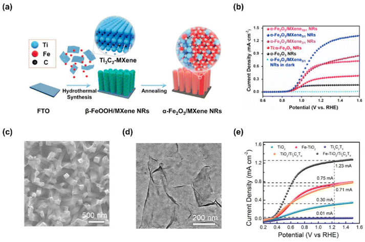
2D MXenes, composed of transition metal carbides, nitrides, and carbonitrides, are obtained by etching “A” element from ternary “MAX” structure, where “M” is a transition metal such as Ti, Mo, V, “A” is Al or Ga, and “X” is C or N.139 Recently, MXene has drawn tremendous attention due to great conductivity, large surface area, exposed active metal sites, and excellent dispersibility enabling them to be utilized in various applications.140–142 Interestingly, the unique 2D MXene analogues such as nitrogen-rich Mo5N6 nanosheets and V0.2Mo0.8N1.2 solid solution have recently been developed for electrochemical HER.143–145 Compared with conventional MXenes, they showed significantly enhanced catalytic activity due to their modified electronic state.Ye et al. successfully designed highly active and stable α-Fe2O3 NRs by coating 2D Ti3C2-MXene using a facile hydrothermal and annealing process.146 In Fig. 10(a), the fabrication of α-Fe2O3/MXene NRs photoanode was shown. Firstly, β-FeOOH/MXene NRs were prepared by hydrothermal method on FTO substrates with a solution of FeCl3, NaNO3, and prepared Ti3C2-MXene. After that, the substrate was washed and heat-treated to prepare α-Fe2O3/MXene NRs. Fig. 11(b) shows the LSV curves of photoanodes produced with various MXene ratios. α-Fe2O3/MXene10/1 NRs with a small amount of MXene produced a photocurrent density of 0.60 mA cm−2 at 1.23 V vs. RHE, which is a four-fold improvement over that of bare hematite NRs. As the atomic ratio of Ti increases, the PEC performance of the photoanode tends to increase, but if the amount of MXene is excessively increased, the growth of nanorods is inhibited, so the PEC performance decreases. As a result, the α-Fe2O3/MXene5/1 NRs produced the largest photocurrent density with a value of 1.10 mA cm−2 at 1.23 V vs. RHE.
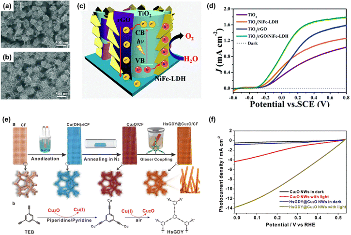
Yin et al. reported an efficient photoanode by depositing Ti3C2Tx MXene on Fe-doped TiO2 nanorod arrays.147 Fe–TiO2 nanorod arrays were prepared by hydrothermal method, and MXene was synthesized by electrodeposition. Fig. 11(c) shows Ti3C2Tx nanosheets adhered well to Fe–TiO2 nanorod arrays after electrodeposition. TEM image of MXene in Fig. 11(d) shows 2D Ti3C2Tx nanosheets with single or several layers which were well exfoliated with a thickness of less than 2.2 nm. The PEC-OER performance of the as-fabricated Fe–TiO2/Ti3C2Tx photoanode can be confirmed in Fig. 11(e). The Fe–TiO2/Ti3C2Tx photoanode, electrodeposited for 240 seconds, showed the best performance with a photocurrent density of 1.23 mA cm−2 at 1. 23 V vs. RHE, which is higher than that of other TiO2-based photoelectrodes. This result is derived from the superiority of Ti3C2Tx nanosheets improving the charge transfer efficiency and water oxidation kinetics of Fe–TiO2.
5. Conclusion and perspective
Solar energy, one of the unlimited energy sources transferred to the earth, can satisfy our desire to produce hydrogen energy without CO2 emission. In this respect, it is necessary to develop inexpensive and high-quality photoelectrodes for low-cost hydrogen production. However, photoelectrode itself can not sufficiently boost the surface reaction, accelerate photogenerated charge transfer, and protect the corrosion. Thus, it is essential to investigate highly catalytic, conductive, and robust materials to support the photoelectrodes. In this review, we summarized the superiorities of 2D materials and introduced the utilization of various 2D materials for photoelectrochemical water splitting. The van der Waals interactions between layers allow them to have unique properties such as large specific surface area, stackability for heterostructure, tunable band gap, and surface functionalization. With these distinctions, they not only support but also act as photoelectrodes. Firstly, their catalytic activity improves the surface reaction producing hydrogen and oxygen. In particular, deliberately enlarged active edge sites and defects contribute to lowering free energy to be required for HER and OER, leading to a low overpotential and high photocurrent density. Also, phase transformation, ion-exchanged sites and synergistically mixed composites enable 2D materials to surpass their intrinsic catalytic activity. Secondly, 2D materials serve as interfacial transporting layers via energetically favorable Schottky junctions, p–n junctions, and multi-heterojunctions as there is no intrinsic surface state within band gap and they can be stacked into substrates without crystal mismatch and atomic interdiffusion. Thirdly, chemically inert 2D materials protect the surface of silicon and oxide-based photoelectrodes vulnerable to the acidic and alkaline electrolyte. Finally, 2D materials having an energy band gap can absorb solar energy and generate electron–hole pairs. Though they intrinsically provide a small amount of photocurrent density, their photoelectrochemical performance can be enhanced by surface treatments and layer stacking.Until now, a variety of 2D materials have been revealed and applied to the field of (photo)electrochemistry. We classified them into transition metal dichalcogenides, carbon allotropes, black phosphorus, layered double hydroxides, g-C3N4, and MXene. Many researchers have strengthened the potential of 2D materials for practical utilization in PEC applications. Despite significant progress in integrating 2D materials into various semiconducting photoabsorbers, there are still issues that must be addressed for the further improvement of the device. Firstly, it is necessary to directly synthesize 2D materials on photoelectrodes with uniformity and large-scale size for practical industrial application. In some research, TMDs and graphene have grown on SiO2 wafer and copper foil, respectively, to obtain high-quality layers. Then, they were transferred on top of photoelectrodes. However, it is not applicable to mass production in which highly uniform and large-scale synthesis should be prioritized. Thus, a technology capable of direct synthesis of 2D materials on photoelectrodes must be developed. Secondly, 2D materials do not chemically adhere to substrates but have physisorption with them, causing a fatal problem that easily falls off during the reaction. As a result, the PEC performance of the device dramatically decreases after desorption. To solve this phenomenon, it is essential to develop a new process that can increase adhesion. Finally, research should be proceeded until the stage of constructing a tandem device for unassisted solar water splitting. If the solar-to-hydrogen efficiency is obtained from a tandem device decorated with 2D materials, the value of 2D materials in the practical industry will be more recognized. We believe that our inclusive review regarding 2D materials for photoelectrochemical water splitting could inspire researchers interested in renewable energy, photoelectrochemical catalysts, and 2D materials.
Author contributions
SE Jun and JK Lee contributed equally to this work. They wrote the manuscript under the supervision of HW Jang. All authors contributed to the general discussion.Conflicts of interest
The authors declare that there are no conflicts of interest.Acknowledgements
This work was supported by the National Research Foundation of Korea (NRF) grant funded by the Korea government Ministry of Science and ICT (MSIT) (2022M3H4A1A01011963). This research was also supported by the KRISS (Korea Research Institute of Standards and Science) MPI Lab. program. The Inter-University Semiconductor Research Center and Institute of Engineering Research at Seoul National University provided research facilities for this work.References
- A. Fujishima and K. Honda, Nature, 1972, 238, 37–38 CrossRef CAS.
- N. S. Lewis and D. G. Nocera, Proc. Natl. Acad. Sci. U. S. A., 2006, 103, 15729–15735 CrossRef CAS PubMed.
- J. Gong, C. Li and M. R. Wasielewski, Chem. Soc. Rev., 2019, 48, 1862–1864 RSC.
- J. Graetz, Chem. Soc. Rev., 2009, 38, 73–82 RSC.
- A. Züttel, Mater. Today, 2003, 6, 24–33 CrossRef.
- P. Chen and M. Zhu, Mater. Today, 2008, 11, 36–43 CrossRef CAS.
- J. J. Alves and G. P. Towler, Ind. Eng. Chem. Res., 2002, 41, 5759–5769 CrossRef CAS.
- N. Armaroli and V. Balzani, ChemSusChem, 2011, 4, 21–36 CrossRef CAS.
- J. O. Abe, A. Popoola, E. Ajenifuja and O. Popoola, Int. J. Hydrogen, 2019, 44, 15072–15086 CrossRef CAS.
- H. Park, I. J. Park, M. G. Lee, K. C. Kwon, S.-P. Hong, D. H. Kim, S. A. Lee, T. H. Lee, C. Kim and C. W. Moon, ACS Appl. Mater. Interfaces, 2019, 11, 33835–33843 CrossRef CAS PubMed.
- H. Park, J. W. Bae, T. H. Lee, I. J. Park, C. Kim, M. G. Lee, S. A. Lee, J. W. Yang, M. J. Choi and S. H. Hong, Small, 2022, 18, 2105611 CrossRef CAS.
- I. Roger, M. A. Shipman and M. D. Symes, Nat. Rev. Chem., 2017, 1, 1–13 CrossRef.
- J. H. Kim, D. Hansora, P. Sharma, J.-W. Jang and J. S. Lee, Chem. Soc. Rev., 2019, 48, 1908–1971 RSC.
- M. R. Shaner, H. A. Atwater, N. S. Lewis and E. W. McFarland, Energy Environ. Sci., 2016, 9, 2354–2371 RSC.
- M. G. Walter, E. L. Warren, J. R. McKone, S. W. Boettcher, Q. Mi, E. A. Santori and N. S. Lewis, Chem. Rev., 2010, 110, 6446–6473 CrossRef CAS PubMed.
- G. Zeng, T. A. Pham, S. Vanka, G. Liu, C. Song, J. K. Cooper, Z. Mi, T. Ogitsu and F. M. Toma, Nat. Mater., 2021, 20, 1130–1135 CrossRef CAS PubMed.
- L. Pan, J. H. Kim, M. T. Mayer, M.-K. Son, A. Ummadisingu, J. S. Lee, A. Hagfeldt, J. Luo and M. Grätzel, Nat. Catal., 2018, 1, 412–420 CrossRef CAS.
- W. Yang, J. H. Kim, O. S. Hutter, L. J. Phillips, J. Tan, J. Park, H. Lee, J. D. Major, J. S. Lee and J. Moon, Nat. Commun., 2020, 11, 1–10 CrossRef PubMed.
- B. Koo, D. Kim, P. Boonmongkolras, S. R. Pae, S. Byun, J. Kim, J. H. Lee, D. H. Kim, S. Kim and B. T. Ahn, ACS Appl. Energy Mater., 2020, 3, 2296–2303 CrossRef CAS.
- S. A. Lee, T. H. Lee, C. Kim, M. G. Lee, M.-J. Choi, H. Park, S. Choi, J. Oh and H. W. Jang, ACS Catal., 2018, 8, 7261–7269 CrossRef CAS.
- S. A. Lee, T. H. Lee, C. Kim, M.-J. Choi, H. Park, S. Choi, J. Lee, J. Oh, S. Y. Kim and H. W. Jang, ACS Catal., 2019, 10, 420–429 CrossRef.
- M. J. Kenney, M. Gong, Y. Li, J. Z. Wu, J. Feng, M. Lanza and H. Dai, Science, 2013, 342, 836–840 CrossRef CAS PubMed.
- X. Yu, P. Yang, S. Chen, M. Zhang and G. Shi, Adv. Energy Mater., 2017, 7, 1601805 CrossRef.
- J. Park, T. H. Lee, C. Kim, S. A. Lee, M.-J. Choi, H. Kim, J. W. Yang, J. Lim and H. W. Jang, Appl. Catal., B, 2021, 295, 120276 CrossRef CAS.
- J. Park, S. Lee, T. H. Lee, C. Kim, S. E. Jun, J. H. Baek, J. Y. Kim, S. H. Ahn and H. W. Jang, Nano Convergence, 2022, 9, 1–14 CrossRef PubMed.
- M. G. Lee, J. W. Yang, H. Park, C. W. Moon, D. M. Andoshe, J. Park, C.-K. Moon, T. H. Lee, K. S. Choi and W. S. Cheon, Nano-Micro Lett., 2022, 14, 1–15 CrossRef.
- M.-J. Choi, T. L. Kim, K. S. Choi, W. Sohn, T. H. Lee, S. A. Lee, H. Park, S. Y. Jeong, J. W. Yang and S. Lee, ACS Appl. Mater. Interfaces, 2022, 14, 7788–7795 CrossRef CAS.
- J. W. Yang, I. J. Park, S. A. Lee, M. G. Lee, T. H. Lee, H. Park, C. Kim, J. Park, J. Moon and J. Y. Kim, Appl. Catal., B, 2021, 293, 120217 CrossRef CAS.
- S. S. Bhat, J. M. Suh, S. Choi, S.-P. Hong, S. A. Lee, C. Kim, C. W. Moon, M. G. Lee and H. W. Jang, J. Mater. Chem. A, 2018, 6, 14633–14643 RSC.
- Y. Zhao, K. R. Yang, Z. Wang, X. Yan, S. Cao, Y. Ye, Q. Dong, X. Zhang, J. E. Thorne and L. Jin, Proc. Natl. Acad. Sci. U. S. A., 2018, 115, 2902–2907 CrossRef CAS.
- S. A. Lee, J. W. Yang, T. H. Lee, I. J. Park, C. Kim, S. H. Hong, H. Lee, S. Choi, J. Moon and S. Y. Kim, Appl. Catal., B, 2022, 121765 CrossRef CAS.
- Z. Luo, T. Wang and J. Gong, Chem. Soc. Rev., 2019, 48, 2158–2181 RSC.
- W. Yang, R. R. Prabhakar, J. Tan, S. D. Tilley and J. Moon, Chem. Soc. Rev., 2019, 48, 4979–5015 RSC.
- D. Bae, B. Seger, P. C. Vesborg, O. Hansen and I. Chorkendorff, Chem. Soc. Rev., 2017, 46, 1933–1954 RSC.
- S. A. Lee, S. Choi, C. Kim, J. W. Yang, S. Y. Kim and H. W. Jang, ACS Mater. Lett., 2019, 2, 107–126 CrossRef.
- E. Zhao, K. Du, P. F. Yin, J. Ran, J. Mao, T. Ling and S. Z. Qiao, Adv. Sci., 2022, 9, 2104363 CrossRef CAS.
- C. Li, Q. Cao, F. Wang, Y. Xiao, Y. Li, J.-J. Delaunay and H. Zhu, Chem. Soc. Rev., 2018, 47, 4981–5037 RSC.
- H. R. Kwon, H. Park, S. E. Jun, S. Choi and H. W. Jang, Chem. Commun., 2022, 58, 7874–7889 RSC.
- Y. Zhu, J. Ren, X. Yang, G. Chang, Y. Bu, G. Wei, W. Han and D. Yang, J. Mater. Chem. A, 2017, 5, 9952–9959 RSC.
- H. Chen, S. Wang, J. Wu, X. Zhang, J. Zhang, M. Lyu, B. Luo, G. Qian and L. Wang, J. Mater. Chem. A, 2020, 8, 13231–13240 RSC.
- C.-J. Chen, V. Veeramani, Y.-H. Wu, A. Jena, L.-C. Yin, H. Chang, S.-F. Hu and R.-S. Liu, Appl. Catal., B, 2020, 263, 118259 CrossRef CAS.
- K. C. Kwon, S. Choi, K. Hong, C. W. Moon, Y.-S. Shim, T. Kim, W. Sohn, J.-M. Jeon, C.-H. Lee and K. T. Nam, Energy Environ. Sci., 2016, 9, 2240–2248 RSC.
- X. Chia and M. Pumera, Nat. Catal., 2018, 1, 909–921 CrossRef CAS.
- A. K. Geim and I. V. Grigorieva, Nature, 2013, 499, 419–425 CrossRef CAS PubMed.
- H. Long, A. Harley-Trochimczyk, T. Pham, Z. Tang, T. Shi, A. Zettl, C. Carraro, M. A. Worsley and R. Maboudian, Adv. Funct. Mater., 2016, 26, 5158–5165 CrossRef CAS.
- A. Chaves, J. G. Azadani, H. Alsalman, D. Da Costa, R. Frisenda, A. Chaves, S. H. Song, Y. D. Kim, D. He, J. Zhou, A. Castellanos-Gomez, F. Peeters, Z. Liu, C. Hinkle, S.-H. Oh, P. D. Ye, S. J. Koester, Y. H. Lee, P. Avouris, X. Wang and T. Low, npj 2D Mater. Appl., 2020, 4, 1–21 CrossRef.
- N. Martín, N. Tagmatarchis, Q. H. Wang and X. Zhang, Chem. – Eur. J., 2020, 26, 6292–6295 CrossRef PubMed.
- Z. Sun, T. Ma, H. Tao, Q. Fan and B. Han, Chem, 2017, 3, 560–587 CAS.
- J. Mao, T. Zhou, Y. Zheng, H. Gao, H. K. Liu and Z. Guo, J. Mater. Chem. A, 2018, 6, 3284–3303 RSC.
- T. H. Eom, S. H. Cho, J. M. Suh, T. Kim, T. H. Lee, S. E. Jun, J. W. Yang, J. Lee, S.-H. Hong and H. W. Jang, J. Mater. Chem. A, 2021, 9, 11168–11178 RSC.
- Z. Li, Z. Zhuang, F. Lv, H. Zhu, L. Zhou, M. Luo, J. Zhu, Z. Lang, S. Feng, W. Chen, L. Mai and S. Guo, Adv. Mater., 2018, 30, 1803220 CrossRef.
- A. R. Fareza, F. A. A. Nugroho, F. F. Abdi and V. Fauzia, J. Mater. Chem. A, 2022, 10, 8656–8686 RSC.
- S. S. M. Bhat, S. A. Pawar, D. Potphode, C.-K. Moon, J. M. Suh, C. Kim, S. Choi, D. S. Patil, J.-J. Kim, J. C. Shin and H. W. Jang, Appl. Catal., B, 2019, 259, 118102 CrossRef CAS.
- S. A. Lee, J. W. Yang, S. Choi and H. W. Jang, Exploration, 2021, 1, 20210012 CrossRef.
- M. Long, P. Wang, H. Fang and W. Hu, Adv. Funct. Mater., 2019, 29, 1803807 CrossRef.
- S. Y. Park, Y. H. Kim, S. Y. Lee, W. Sohn, J. E. Lee, D. H. Kim, Y.-S. Shim, K. C. Kwon, K. S. Choi, H. J. Yoo, J. M. Suh, M. Ko, J.-H. Lee, M. J. Lee, S. Y. Kim, M. H. Lee and H. W. Jang, J. Mater. Chem. A, 2018, 6, 5016–5024 RSC.
- Y. Wang, J. Pang, Q. Cheng, L. Han, Y. Li, X. Meng, B. Ibarlucea, H. Zhao, F. Yang, H. Liu, H. Liu, W. Zhou, X. Wang, M. H. Rummeli, Y. Zhang and G. Cuniberti, Nano-Micro Lett., 2021, 13, 143 CrossRef CAS PubMed.
- A. M. Smith and S. Nie, Acc. Chem. Res., 2010, 43, 190–200 CrossRef CAS PubMed.
- C. Zhang, H. Huang, X. Ni, Y. Zhou, L. Kang, W. Jiang, H. Chen, J. Zhong and F. Liu, Nanoscale, 2018, 10, 16759–16764 RSC.
- A. Ramasubramaniam, D. Naveh and E. Towe, Nano Lett., 2011, 11, 1070–1075 CrossRef CAS PubMed.
- S. Manzeli, A. Allain, A. Ghadimi and A. Kis, Nano Lett., 2015, 15, 5330–5335 CrossRef CAS PubMed.
- J. Wan, S. D. Lacey, J. Dai, W. Bao, M. S. Fuhrer and L. Hu, Chem. Soc. Rev., 2016, 45, 6742–6765 RSC.
- Y. Gong, Z. Liu, A. R. Lupini, G. Shi, J. Lin, S. Najmaei, Z. Lin, A. L. Elías, A. Berkdemir, G. You, H. Terrones, M. Terrones, R. Vajtai, S. T. Pantelides, S. J. Pennycook, J. Lou, W. Zhou and P. M. Ajayan, Nano Lett., 2014, 14, 442–449 CrossRef CAS PubMed.
- Y. Chen, J. Xi, D. O. Dumcenco, Z. Liu, K. Suenaga, D. Wang, Z. Shuai, Y.-S. Huang and L. Xie, ACS Nano, 2013, 7, 4610–4616 CrossRef CAS PubMed.
- G. Gui, J. Li and J. Zhong, Phys. Rev. B: Condens. Matter Mater. Phys., 2008, 78, 075435 CrossRef.
- Z. H. Ni, T. Yu, Y. H. Lu, Y. Y. Wang, Y. P. Feng and Z. X. Shen, ACS Nano, 2008, 2, 2301–2305 CrossRef CAS PubMed.
- Z. Wang, P. Liu, Y. Ito, S. Ning, Y. Tan, T. Fujita, A. Hirata and M. Chen, Sci. Rep., 2016, 6, 1–9 CrossRef PubMed.
- L. Daukiya, J. Seibel and S. De Feyter, Adv. Phys.: X, 2019, 4, 1625723 CAS.
- S. Presolski and M. Pumera, Mater. Today, 2016, 19, 140–145 CrossRef CAS.
- A. R. Brill, E. Koren and G. de Ruiter, J. Mater. Chem. C, 2021, 9, 11569–11587 RSC.
- C. Liu, C. Kong, F.-J. Zhang, C.-M. Kai, W.-Q. Cai, X.-Y. Sun and W.-C. Oh, J. Korean Ceram. Soc., 2021, 58, 135–147 CrossRef CAS.
- M. G. Lee, J. W. Yang, H. R. Kwon and H. W. Jang, CrystEngComm, 2022, 24, 5838–5864 RSC.
- B. You, M. T. Tang, C. Tsai, F. Abild-Pedersen, X. Zheng and H. Li, Adv. Mater., 2019, 31, 1807001 CrossRef PubMed.
- J. Huang, H. Gao, Y. Xia, Y. Sun, J. Xiong, Y. Li, S. Cong, J. Guo, S. Du and G. Zou, Nano Energy, 2018, 46, 305–313 CrossRef CAS.
- J. Zhang, X. Xu, L. Yang, D. Cheng and D. Cao, Small Methods, 2019, 3, 1900653 CrossRef CAS.
- H. Li, C. Tsai, A. L. Koh, L. Cai, A. W. Contryman, A. H. Fragapane, J. Zhao, H. S. Han, H. C. Manoharan, A.-P. Frank and J. K. Nørskov, Nat. Mater., 2016, 15, 48–53 CrossRef CAS PubMed.
- C. Tsai, H. Li, S. Park, J. Park, H. S. Han, J. K. Nørskov, X. Zheng and F. Abild-Pedersen, Nat. Commun., 2017, 8, 1–8 CrossRef PubMed.
- T. F. Jaramillo, K. P. Jørgensen, J. Bonde, J. H. Nielsen, S. Horch and I. Chorkendorff, Science, 2007, 317, 100–102 CrossRef CAS PubMed.
- R. Fan, J. Mao, Z. Yin, J. Jie, W. Dong, L. Fang, F. Zheng and M. Shen, ACS Appl. Mater. Interfaces, 2017, 9, 6123–6129 CrossRef CAS PubMed.
- S. E. Jun, S. P. Hong, S. Choi, C. Kim, S. G. Ji, I. J. Park, S. A. Lee, J. W. Yang, T. H. Lee, W. Sohn, J. Y. Kim and H. W. Jang, Small, 2021, 17, 2103457 CrossRef CAS PubMed.
- J. W. Hill, Z. Fu, J. Tian and C. M. Hill, J. Phys. Chem. C, 2020, 124, 17141–17149 CrossRef CAS.
- W. Huang, Q. Zhou, S. Su, J. Li, X. Lu, X. Gao, X. Wang, M. Jin, G. Zhou, Z. Zhang and J. Liu, Adv. Mater. Interfaces, 2019, 6, 1801663 CrossRef.
- D. Voiry, A. Mohite and M. Chhowalla, Chem. Soc. Rev., 2015, 44, 2702–2712 RSC.
- Z. Lei, J. Zhan, L. Tang, Y. Zhang and Y. Wang, Adv. Energy Mater., 2018, 8, 1703482 CrossRef.
- F. Xiong, H. Wang, X. Liu, J. Sun, M. Brongersma, E. Pop and Y. Cui, Nano Lett., 2015, 15, 6777–6784 CrossRef CAS PubMed.
- X. Wang, X. Shen, Z. Wang, R. Yu and L. Chen, ACS Nano, 2014, 8, 11394–11400 CrossRef CAS PubMed.
- Z. Lai, Y. Yao, S. Li, L. Ma, Q. Zhang, Y. Ge, W. Zhai, B. Chi, B. Chen, L. Li, L. Wang, Z. Zheng, L. Gu, Y. Du and H. Zhang, Adv. Mater., 2022, 2201194 CrossRef CAS PubMed.
- Q. Ding, F. Meng, C. R. English, M. Cabán-Acevedo, M. J. Shearer, D. Liang, A. S. Daniel, R. J. Hamers and S. Jin, J. Am. Chem. Soc., 2014, 136, 8504–8507 CrossRef CAS PubMed.
- K. C. Kwon, S. Choi, J. Lee, K. Hong, W. Sohn, D. M. Andoshe, K. S. Choi, Y. Kim, S. Han, S. Y. Kim and H. W. Jang, J. Mater. Chem. A, 2017, 5, 15534–15542 RSC.
- S. Choi, C. Kim, J. Y. Lee, T. H. Lee, K. C. Kwon, S. Kang, S. A. Lee, K. S. Choi, J. M. Suh, K. Hong, S. E. Jun, W. K. Kim, S. H. Ahn, S. Han, S. Y. Kim, C.-H. Lee and H. W. Jang, Chem. Eng. J., 2021, 418, 129369 CrossRef CAS.
- J. E. Thorne, Y. Zhao, D. He, S. Fan, S. Vanka, Z. Mi and D. Wang, Phys. Chem. Chem. Phys., 2017, 19, 29653–29659 RSC.
- G. Yang, S. Li, X. Wang, B. Ding, Y. Li, H. Lin, D. Tang, X. Ren, Q. Wang, S. Luo and J. Ye, Appl. Catal., B, 2021, 297, 120268 CrossRef CAS.
- C. K. Ku, P. H. Wu, C. C. Chung, C. C. Chen, K. J. Tsai, H. M. Chen, Y. C. Chang, C. H. Chuang, C. Y. Wei, C. Y. Wen, T.-Y. Lin, H.-L. Chen, Y.-S. Wang, Z.-Y. Lee, J.-R. Chang, C.-W. Luo, D.-Y. Wang, B. J. HWang and C.-W. Chen, Adv. Energy Mater., 2019, 9, 1901022 CrossRef.
- K. C. Kwon, S. Choi, K. Hong, C. W. Moon, Y.-S. Shim, T. Kim, W. Sohn, J.-M. Jeon, C.-H. Lee, K. T. Nam, S. Han, S. Y. Kim and H. W. Jang, Energy Environ. Sci., 2016, 9, 2240–2248 RSC.
- D. Ghosh, P. Devi and P. Kumar, ACS Appl. Mater. Interfaces, 2020, 12, 13797–13804 CrossRef CAS PubMed.
- S. Seo, S. Kim, H. Choi, J. Lee, H. Yoon, G. Piao, J. C. Park, Y. Jung, J. Song, S. Y. Jeong, H. Park and S. Lee, Adv. Sci., 2019, 6, 1900301 CrossRef PubMed.
- S. E. Jun, S. Choi, S. Choi, T. H. Lee, C. Kim, J. W. Yang, W.-O. Choe, I.-H. Im, C.-J. Kim and H. W. Jang, Nano-Micro Lett., 2021, 13, 1–16 Search PubMed.
- U. Sim, T.-Y. Yang, J. Moon, J. An, J. Hwang, J.-H. Seo, J. Lee, K. Y. Kim, J. Lee, S. Han, B. H. Hong and K. T. Nam, Energy Environ. Sci., 2013, 6, 3658–3664 RSC.
- L. A. King, T. R. Hellstern, J. Park, R. Sinclair and T. F. Jaramillo, ACS Appl. Mater. Interfaces, 2017, 9, 36792–36798 CrossRef CAS PubMed.
- X. Yu, N. Guijarro, M. Johnson and K. Sivula, Nano Lett., 2018, 18, 215–222 CrossRef CAS PubMed.
- L. Wang, M. Tahir, H. Chen and J. B. Sambur, Nano Lett., 2019, 19, 9084–9094 CrossRef CAS PubMed.
- B. Zhou, X. Kong, S. Vanka, S. Chu, P. Ghamari, Y. Wang, N. Pant, I. Shih, H. Guo and Z. Mi, Nat. Commun., 2018, 9, 1–8 CrossRef PubMed.
- K. C. Kwon, S. Choi, K. Hong, D. M. Andoshe, J. M. Suh, C. Kim, K. S. Choi, J. H. Oh, S. Y. Kim and H. W. Jang, MRS Commun., 2017, 7, 272–279 CrossRef CAS.
- P. Gnanasekar, D. Periyanagounder, P. Varadhan, J.-H. He and J. Kulandaivel, ACS Appl. Mater. Interfaces, 2019, 11, 44179–44185 CrossRef CAS PubMed.
- C.-C. Chung, H. Yeh, P.-H. Wu, C.-C. Lin, C.-S. Li, T.-T. Yeh, Y. Chou, C.-Y. Wei, C.-Y. Wen and Y.-C. Chou, ACS Nano, 2021, 15, 4627–4635 CrossRef CAS PubMed.
- W. Huang, Q. Zhou, S. Su, J. Li, X. Lu, X. Gao, X. Wang, M. Jin, G. Zhou and Z. Zhang, Adv. Mater. Interfaces, 2019, 6, 1801663 CrossRef.
- D. M. Andoshe, G. Jin, C. S. Lee, C. Kim, K. C. Kwon, S. Choi, W. Sohn, C. W. Moon, S. H. Lee and J. M. Suh, Adv. Sustainable Syst., 2018, 2, 1700142 CrossRef.
- A. Hasani, Q. Van Le, M. Tekalgne, M.-J. Choi, S. Choi, T. H. Lee, H. Kim, S. H. Ahn, H. W. Jang and S. Y. Kim, ACS Appl. Mater. Interfaces, 2019, 11, 29910–29916 CrossRef CAS PubMed.
- Y. Liu, J. Wu, K. P. Hackenberg, J. Zhang, Y. M. Wang, Y. Yang, K. Keyshar, J. Gu, T. Ogitsu and R. Vajtai, Nat. Energy, 2017, 2, 1–7 CrossRef PubMed.
- K. S. Novoselov, A. K. Geim, S. V. Morozov, D.-E. Jiang, Y. Zhang, S. V. Dubonos, I. V. Grigorieva and A. A. Firsov, Science, 2004, 306, 666–669 CrossRef CAS PubMed.
- Y. Zhang, Y.-W. Tan, H. L. Stormer and P. Kim, Nature, 2005, 438, 201–204 CrossRef CAS PubMed.
- A. A. Balandin, Nat. Mater., 2011, 10, 569–581 CrossRef CAS PubMed.
- R. R. Nair, P. Blake, A. N. Grigorenko, K. S. Novoselov, T. J. Booth, T. Stauber, N. M. Peres and A. K. Geim, Science, 2008, 320, 1308 CrossRef CAS PubMed.
- X. Du, I. Skachko, A. Barker and E. Y. Andrei, Nat. Nanotechnol., 2008, 3, 491–495 CrossRef CAS PubMed.
- C. Lee, X. Wei, J. W. Kysar and J. Hone, Science, 2008, 321, 385–388 CrossRef CAS PubMed.
- X. Li, J. Yu, S. Wageh, A. A. Al-Ghamdi and J. Xie, Small, 2016, 12, 6640–6696 CrossRef CAS PubMed.
- U. Sim, J. Moon, J. An, J. H. Kang, S. E. Jerng, J. Moon, S.-P. Cho, B. H. Hong and K. T. Nam, Energy Environ. Sci., 2015, 8, 1329–1338 RSC.
- F.-X. Xiao, J. Miao and B. Liu, J. Am. Chem. Soc., 2014, 136, 1559–1569 CrossRef CAS PubMed.
- K.-Y. Yoon, J.-S. Lee, K. Kim, C. H. Bak, S.-I. Kim, J.-B. Kim and J.-H. Jang, ACS Appl. Mater. Interfaces, 2014, 6, 22634–22639 CrossRef CAS PubMed.
- S. Chandrasekaran, J. S. Chung, E. J. Kim and S. H. Hur, Chem. Eng. J., 2016, 290, 465–476 CrossRef CAS.
- U. Sim, J. Moon, J. Lee, J. An, H.-Y. Ahn, D. J. Kim, I. Jo, C. Jeon, S. Han and B. H. Hong, ACS Appl. Mater. Interfaces, 2017, 9, 3570–3580 CrossRef CAS PubMed.
- F. Ning, M. Shao, S. Xu, Y. Fu, R. Zhang, M. Wei, D. G. Evans and X. Duan, Energy Environ. Sci., 2016, 9, 2633–2643 RSC.
- X. Gao, H. Liu, D. Wang and J. Zhang, Chem. Soc. Rev., 2019, 48, 908–936 RSC.
- H. Yu, Y. Xue and Y. Li, Adv. Mater., 2019, 31, 1803101 CrossRef CAS PubMed.
- S. Zhang, C. Yin, Z. Kang, P. Wu, J. Wu, Z. Zhang, Q. Liao, J. Zhang and Y. Zhang, ACS Appl. Mater. Interfaces, 2018, 11, 2745–2749 CrossRef PubMed.
- X. Zhou, B. Fu, L. Li, Z. Tian, X. Xu, Z. Wu, J. Yang and Z. Zhang, Nat. Commun., 2022, 13, 1–10 Search PubMed.
- H. Liu, Y. Du, Y. Deng and D. Y. Peide, Chem. Soc. Rev., 2015, 44, 2732–2743 RSC.
- L. Zheng, X. Ye, X. Deng, Y. Wang, Y. Zhao, X. Shi and H. Zheng, ACS Sustainable Chem. Eng., 2020, 8, 15906–15914 CrossRef CAS.
- K. Zhang, B. Jin, C. Park, Y. Cho, X. Song, X. Shi, S. Zhang, W. Kim, H. Zeng and J. H. Park, Nat. Commun., 2019, 10, 1–10 CrossRef PubMed.
- J. Han, Y. Dou, J. Zhao, M. Wei, D. G. Evans and X. Duan, Small, 2013, 9, 98–106 CrossRef CAS PubMed.
- A. I. Khan and D. O’Hare, J. Mater. Chem., 2002, 12, 3191–3198 RSC.
- R. Chong, B. Wang, C. Su, D. Li, L. Mao, Z. Chang and L. Zhang, J. Mater. Chem. A, 2017, 5, 8583–8590 RSC.
- S. Choi, S. A. Lee, H. Yang, T. H. Lee, C. Kim, C. W. Lee, H. Shin and H. W. Jang, ACS Appl. Energy Mater., 2020, 3, 12298–12307 CrossRef CAS.
- L. Jiang, X. Yuan, Y. Pan, J. Liang, G. Zeng, Z. Wu and H. Wang, Appl. Catal., B, 2017, 217, 388–406 CrossRef CAS.
- Y. Li, R. Wang, H. Li, X. Wei, J. Feng, K. Liu, Y. Dang and A. Zhou, J. Phys. Chem. C, 2015, 119, 20283–20292 CrossRef CAS.
- S. S. Bhat, S. E. Jun, S. A. Lee, T. H. Lee and H. W. Jang, Energies, 2020, 13, 974 CrossRef CAS.
- P. Wen, Y. Sun, H. Li, Z. Liang, H. Wu, J. Zhang, H. Zeng, S. M. Geyer and L. Jiang, Appl. Catal., B, 2020, 263, 118180 CrossRef CAS.
- B. Jiang, H. Huang, W. Gong, X. Gu, T. Liu, J. Zhang, W. Qin, H. Chen, Y. Jin and Z. Liang, Adv. Funct. Mater., 2021, 31, 2105045 CrossRef CAS.
- M. Naguib, M. Kurtoglu, V. Presser, J. Lu, J. Niu, M. Heon, L. Hultman, Y. Gogotsi and M. W. Barsoum, Adv. Mater., 2011, 23, 4248–4253 CrossRef CAS PubMed.
- H. Huang, J. Cui, G. Liu, R. Bi and L. Zhang, ACS Nano, 2019, 13, 3448–3456 CrossRef CAS PubMed.
- X. Fan, Y. Ding, Y. Liu, J. Liang and Y. Chen, ACS Nano, 2019, 13, 8124–8134 CrossRef CAS PubMed.
- H.-S. Lim, S. B. Choi, H. Kwon, J.-W. Lim, C. J. Han, J.-M. Oh and J.-W. Kim, Electron. Mater. Lett., 2021, 17, 513–520 CrossRef CAS.
- H. Jin, H. Yu, H. Li, K. Davey, T. Song, U. Paik and S. Z. Qiao, Angew. Chem., Int. Ed., 2022, e202203850 CAS.
- H. Jin, X. Liu, A. Vasileff, Y. Jiao, Y. Zhao, Y. Zheng and S.-Z. Qiao, ACS Nano, 2018, 12, 12761–12769 CrossRef CAS PubMed.
- H. Jin, T. Song, U. Paik and S.-Z. Qiao, Acc. Mater. Res., 2021, 2, 559–573 CrossRef CAS.
- R.-K. Ye, S.-S. Sun, L.-Q. He, S.-R. Yang, X.-Q. Liu, P.-P. Fang and J.-Q. Hu, Appl. Catal., B, 2021, 291, 120107 CrossRef CAS.
- H. Yin, Y. Wang, L. Ma, S. Zhang, B. Yang and R. Jiang, Chem. Eng. J., 2022, 431, 134124 CrossRef CAS.
Footnote |
| † These authors contributed equally to this work. |
| This journal is © The Royal Society of Chemistry 2023 |


