
 Open Access Article
 This Open Access Article is licensed under a Creative Commons Attribution-Non Commercial 3.0 Unported Licence
Graphene-like emerging 2D materials: recent progress, challenges and future outlook
Md. Mohi Uddin*a,
Mohammad Humaun Kabira,
Md. Ashraf Ali a,
Md. Mukter Hossaina,
Mayeen Uddin Khandaker*bc,
Sumit Mandald,
A. Arifutzzamane and
Debnarayan Janaf
a,
Md. Mukter Hossaina,
Mayeen Uddin Khandaker*bc,
Sumit Mandald,
A. Arifutzzamane and
Debnarayan Janaf
aDepartment of Physics, Chittagong University of Engineering and Technology, Chattogram-4349, Bangladesh. E-mail: mohi@cuet.ac.bd; mkhumaun@cuet.ac.bd; ashrafphy31@cuet.ac.bd; mukter_phy@cuet.ac.bd
bFaculty of Graduate Studies, Daffodil International University, Daffodil Smart City, Birulia, Savar, Dhaka 1216, Bangladesh. E-mail: mayeenk@diu.edu.bd
cCentre for Applied Physics and Radiation Technologies, School of Engineering and Technology, Sunway University, 47500 Bandar Sunway, Selangor, Malaysia
dVidyasagar College, 39, Sankar Ghosh Lane, Kolkata, 700006, West Bengal, India. E-mail: smtdone@gmail.com
eTyndall National Institute, University College Cork, Lee Maltings, Cork, T12 R5CP, Ireland. E-mail: arifutzzaman.rahat@tyndall.ie
fDepartment of Physics, University of Calcutta, 92 A P C Road, Kolkata, 700009, West Bengal, India. E-mail: djphy@caluniv.ac.in
First published on 13th November 2023
Abstract
Owing to the unique physical and chemical properties of 2D materials and the great success of graphene in various applications, the scientific community has been influenced to explore a new class of graphene-like 2D materials for next-generation technological applications. Consequently, many alternative layered and non-layered 2D materials, including h-BN, TMDs, and MXenes, have been synthesized recently for applications related to the 4th industrial revolution. In this review, recent progress in state-of-the-art research on 2D materials, including their synthesis routes, characterization and application-oriented properties, has been highlighted. The evolving applications of 2D materials in the areas of electronics, optoelectronics, spintronic devices, sensors, high-performance and transparent electrodes, energy conversion and storage, electromagnetic interference shielding, hydrogen evolution reaction (HER), oxygen evolution reaction (OER), and nanocomposites are discussed. In particular, the state-of-the-art applications, challenges, and outlook of every class of 2D material are also presented as concluding remarks to guide this fast-progressing class of 2D materials beyond graphene for scientific research into next-generation materials.
1. Introduction
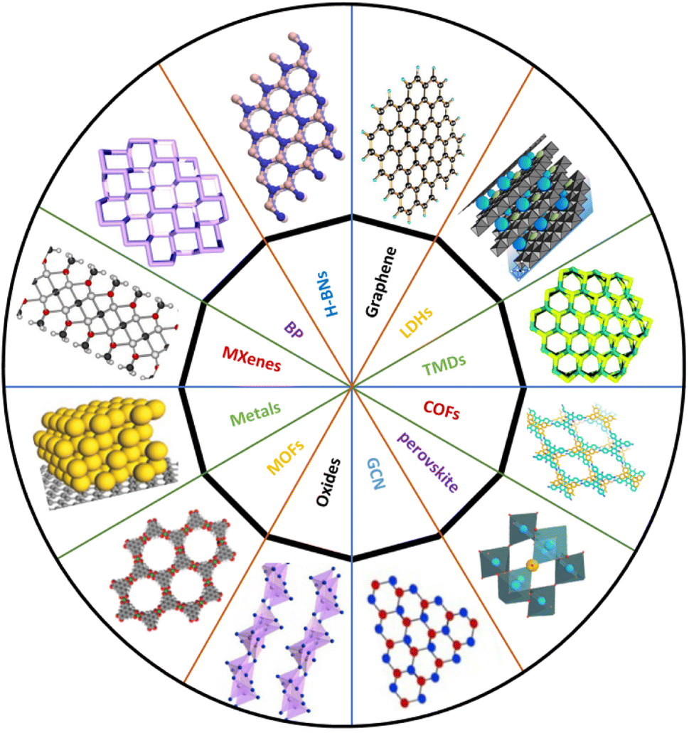
We are currently in the age of nanotechnology that is the basis of technological evolution and where the innovation of more sustainable and economical unique materials has noticeably increased. After the discovery of graphene with its physiochemical properties and applications, the door has opened to a world of 2D materials due to their extraordinary properties that have become an extensive area of research in recent years.1–3 Advances in graphene applications and fundamental studies have attracted scientists to develop a surfeit of 2D materials and to search for new members of the 2D family. Remarkably, the collection of 2D-layered materials are among the most widely studied materials due to their unique physical peculiarities and a considerable number of new materials are now being provided and added to the list every year; currently the family has more than 150 members.In 2004, scientists were first able to isolate a single-layer plane of graphene using the adhesive tape technique and graphene showed unique and exciting electronic properties.4,5 This success aroused huge interest in the large-scale production of 2D materials. Over the last decade, scientists have successfully exfoliated van der Waals materials (both chemically and mechanically) into single and few layers.6 This technique has elaborated the field of 2D materials beyond graphene and given birth to many ‘cousins’, as shown in Fig. 1, such as hexagonal boron nitride (h-BN), black phosphorus (BP), transition metal dichalcogenides (TMDs, MX2), metal–organic frameworks (MOFs), layered double hydroxides (LDHs), covalent organic frameworks (COFs), a family of monoelemental compounds (Xenes), metal oxides, graphitic carbon nitride (g-C3N4), metal nitrides/carbides (MXenes), 12–15 transition metal halides (TMHs) (e.g., PbI2 and MgBr2), perovskite-type oxides (e.g., K2Ln2Ti3O10 and RbLnTa2O7 (Ln: lanthanide ion)), and 2D polymers.
 | ||
| Fig. 1 Illustration of different kinds of typical 2D materials. | ||
Graphene, a previously isolated carbon material, is acting as a building block to search for other family members based on dimensionality. Single-layered TMDs have attracted devotion due to their natural abundance and assorted applications. TMDs with the chemical formula MX2 (where M is a transition metal from groups 4–10, such as Mo, Nb, W, Ni, V, or Re, and X is a chalcogen such as Se, Te, or S).6–9 Currently, 40 various combinations of TMDs with different chalcogen atoms have been revealed, as illustrated in Fig. 2(a). TMDs exhibit a variety of structures according to the oxidation state of their atoms and coordination number such as metals (NbSe2 shows a superconductivity effect at low temperature),10–12 semimetals (TiSe2),13 semiconductors (MoS2)14 and insulators (HfS2).5
 | ||
| Fig. 2 (a) Current members of the 2D graphene-like layered structure family.6 Blue shading depicts materials that are stable under ambient conditions (room temperature in air). Green-shaded materials are probably stable in air; pink-shaded ones may be stable in an inert atmosphere but are probably unstable in air. Grey shading designates 3D compounds that have been successfully exfoliated down to monolayers, as confirmed by atomic force microscopy. Reproduced from ref. 15 with permission from Springer Nature, copyright 2013. (b) MXenes can have at least four different formulas: M2X, M3X2, M4X3, M5X4, where M is an early transition metal and X is carbon and/or nitrogen. They can be made in three different forms: mono-M elements (for example, Ti2C and Nb4C3); a solid solution of at least two different M elements (for example, (Ti, V)); or ordered double-M elements, in which one transition metal occupies the perimeter layers and another fills the central M layers (for example, Mo2TiC2 and Mo2Ti2C, in which the outer M layers are Mo and the central M layers are Ti). Solid solutions on the X site produce carbonitrides. Reproduced from ref. 15 with permission from Springer Nature, copyright 2017. | ||
Intense research efforts have been put into the fast development of abundant synthesized compositions. Hexagonal boron nitride (h-BN), metal chalcogenides, metal oxides, metal halides, metal carbides/nitrides (MXenes), and organic semiconductors (OSCs) are considered prospective 2D materials based on their diverse applications in different devices. Almost all the atoms on the surface of these materials are exposed after exfoliation (ultrathin form); thus, the surface areas of 2D materials are noticeably increased, which significantly increases their physical and chemical reactivity and influences the 2D work function through quantum confinement effects. To date, about 30 MXene-based compositions have been reported (shown by the blue color in Fig. 2(b)), and several others have been surveyed through computational means (shown by the gray color in Fig. 2(b)).
2D materials exhibit novel and exciting properties, so that people are expecting many innovative openings. This review emphasizes the highest degree of development of graphene-like materials. First, we will introduce the overview, classification, and characterization of 2D materials followed by the properties of 2D materials. We also discuss in detail the synthesis routes of each class of 2D material along with the basic principles and importance of emerging techniques for their elite applications and experimental guidance for distinguishing and describing single or multilayer materials. We detail the challenges and future research directions for each class of 2D materials in the respective sections for a better understanding of what needs to be fixed to accelerate their emerging applications. Finally, we elucidate various newly developed 2D materials, their properties and prospects of single and multilayers and many layers in field-effect transistors, energy conversion and storage, electrochemical performance and many other applications.
2. Synthesis methods for 2D materials
Nucleation and growth regulate the main mechanism of conventional crystal development16 and the arrangement of atomic order deemed to be the stable state, as shown in Fig. 3(a). Modern scientists have discovered that an amorphous precursor may be a crucial transitional outcome in the process of crystal formation, particularly in bio-mineralization.17 At the beginning, they may accumulate prior to nucleation for prevailing scattered atomic organization, as shown in Fig. 3(b). Therefore, hindering the conversion from amorphous to crystal phase is the main phenomenon in the synthesis of amorphous materials. It is found in the literature that coordination/adsorption18 and lattice distortion19 among others are the possible alternative routes for the fabrication of amorphous 2D nanomaterials.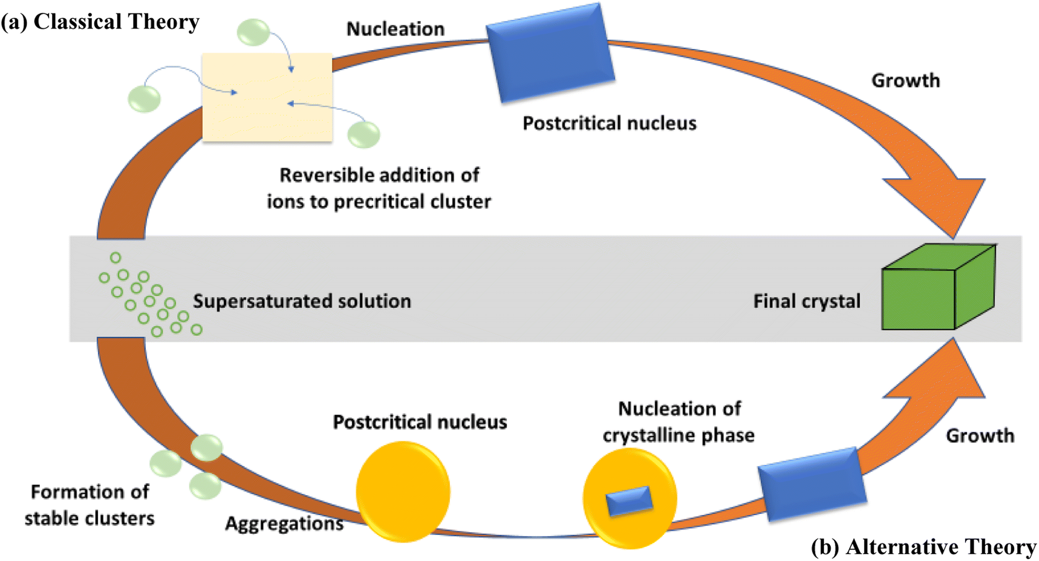 | ||
| Fig. 3 Schematic sketch of conventional (a) and non-conventional (b) nucleation principles. Reproduced from ref. 17 with permission from Elsevier, copyright 2011. | ||
Essentially, these techniques are classified into two major types: top-down and bottom-up processes. In the top-down method, the 2D membrane of the materials is achieved through by breaking down the respective bulk precursors by adopting different physical or chemical techniques: the Scotch-tape method, chemical exfoliation, etc. In practice, the top-down method can synthesise nearly all compounds as 2D structures. On the other hand, bottom-up methods involve atom-by atom, molecule-by-molecule or cluster-by-cluster manipulation for the synthesis of nanostructures. Typical bottom-up methods, include laser deposition, ion exchange, electro-deposition, phase transformation, solvothermal colloidal chemistry techniques and 2D-structured synthesis, all of which depend on chemical reactions in certain experimental environments. 2D materials produced using different synthesis methods or techniques are later discussed with special care in their own sections.
3. Characterization methods for 2D materials
Numerous characterization techniques and protocols have been presented in different papers published by the 2D material research community. This is because the fundamental characterization paths are essential for ensuring the reproducibility of the as-produced materials.21 However, out-of-plane physical structures of 2D nanomaterials have a great impact on their various optical characteristics that could be investigated by the different microscopy methods. Various methods for the characterization of 2D nanomaterials have been implemented, such as structural analysis by X-ray diffraction (XRD), surface morphology analysis with the aid of various electron microscopy techniques, such as SEM, TEM, STM, STEM, and tip-enhanced Raman spectroscopy (TERS). TERS is a variant of surface enhanced Raman spectroscopy (SERS) and it combines scanning probe microscopy and Raman spectroscopy. High spatial resolution, including nanometer spatial resolution, is possible in TERS. In addition, elemental and chemical composition analysis via EDX, EELS and atomic force microscopy (AFM), Raman spectroscopy, and photoluminescence (PL) spectroscopy has been widely implemented. For preference, to obtain trustworthy data, more than one characterization technique should be implemented. For example, it is essential to employ dynamic light scattering (DLS) in combination with SEM to confirm the distribution of particle sizes. On the other hand, the attributes acquired from a certain synthesis technique could be used to estimate the discrepancies between routes and to identify the best synthesis route for a particular application.4. Properties of 2D materials
Simple ultrathin nanoparticles with significant chemical functionality and anisotropy make up two-dimensional (2D) materials. Both heat and charge transfer are restricted to one plane in such materials. They also have a huge specific surface area, a distinct optical bandgap, and strong light–matter interactions. How much of a material is exposed to the ambient surroundings is determined by its surface area (S) to volume (V) ratio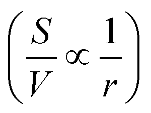 . The all-surface structure of these 2D materials provides the ability to modify their characteristics by chemical functionalization: a surface treatment. Due to this, 2D materials appear to be far more reactive than their bulk equivalents.
The origin of the new properties of these 2D materials is due to the modifications of their electronic band structure and the intriguing nature of the bonds between their atoms. Due to strong covalent bonding, the materials provide good in-plane stability. However, the out-of-plane interactions makes them excellent for monolayer isolation of a 2D single layer due to weak van der Waals interlayered interactions.6,22–24 Therefore, relative to bulk excitons, the bandgap and exciton binding energy will rise as a result of electron quantum confinement. Due to electron confinement and the lack of interlayer interactions, the optical and electrical characteristics of these 2D materials are entirely distinct from those of the bulk materials.25–27 Chemical functionalization flaws, strain,28 and electric fields may all change the structural, electrical, optical, and chemical characteristics of these materials. Additionally, 2D materials inspired by graphene are receiving a lot of interest due to their unique electrical architectures.29–31
In Fig. 4, we schematically highlight the electronic band parameters of a few selected 2D materials which may be important for future applications in nanodevices.
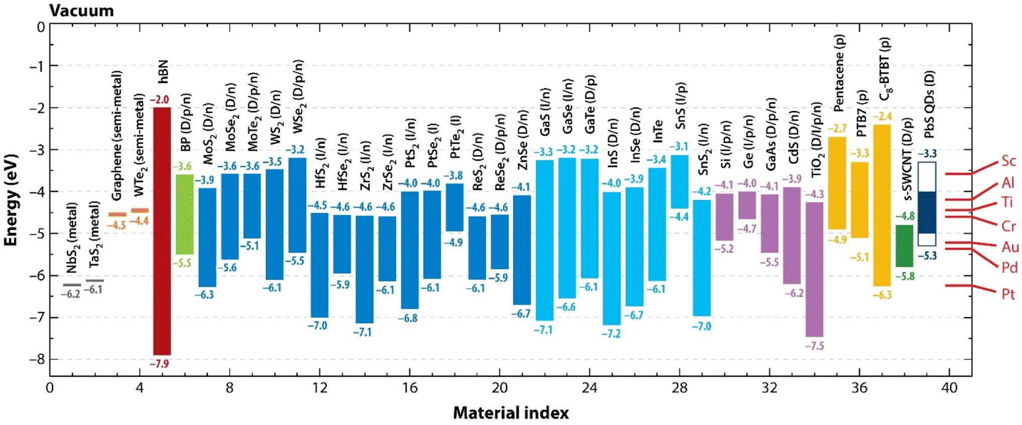 | ||
| Fig. 4 Properties of the electronic bands of selected 2D materials. The positions of the valence band maxima and conduction band minima with respect to vacuum for the selected 2D monolayers and ordinary semiconductors. Metals and semimetals are covered by the work function. Materials are categorized according to colour as follows: 2D metals: dark grey (material index 1, 2); 2D semimetals: orange (3, 4); hBN: dark red (5); black phosphorus (BP): green (6); 1H transition metal dichalcogenides: blue (7–21); post-transition-metal chalcogenides: cyan (22–29); inorganic semiconductors: purple (30–34); organic semiconductors: yellow (35–37); s-SWCNT: dark green (38); PbS QDs: dark blue (39). (Right) The work functions of typical metal contacts are shown by red lines. p = mainly hole conduction; n = predominantly electron conduction; p/n = both electron and hole conduction or ambipolar conduction; D = direct bandgap; I = indirect bandgap; D/I = both direct and indirect gaps are conceivable depending on phase. If the electron affinity (CB) for monolayers is unavailable, the bulk is used to get this value. Electronic bandgaps are depicted when there are significant discrepancies between the optical and electronic bandgaps (for example, 1.8 vs. 2.4 eV for MoS2, respectively). Reproduced from ref. 32 with permission. | ||
4.1 Graphene and graphene-like 2D materials
Since the publication of Geim and Novoselov's research in 2004, the area of graphene science and technology has grown considerably. However, technological progress is dependent not just on fundamental research but also on the emergence of novel industrial-scale production methods for graphene. Even though mechanically exfoliated graphene, such as that created by the Scotch-tape method, has the greatest physical qualities, the cost of producing individual flakes using this approach prevents it from being used in bulk manufacturing. Also, graphene being a semimetal, has no energy bandgap. Thus, fabricating electronic devices that can actually turn off is a challenge. However, techniques for opening a bandgap have been developed over the years, but they resulted in sophistication at the cost of the robustness of the graphene membrane. Compared to graphene, graphene derivatives are Eg-tunable and relatively low-cost materials that involve less complex fabrication methods.33
4.1.2.1 Synthesis of GO. A tried-and-true method for producing graphene-based materials is the oxidation of graphite powder to graphene oxide (GO), followed by a suitable chemical reduction to reduced graphene oxide (r-GO).37 Many potent chemical oxidants have been regularly utilized to create graphene oxide from flaked graphite as a starting material.38 The reduction of graphene oxide to compounds that resemble graphene is one of the most significant chemical transformations. In addition to its reduction, graphene oxide provides an easy method for creating functionalized graphene platelets, which may exhibit enhanced mechanical, thermal, and/or electrical characteristics.
To mention a few techniques, Tour and colleagues reported39,40 an improvement on Hummers' approach using ice instead of liquid water to avoid a large temperature increase and eliminating NaNO3 to prevent the production of poisonous gases.41 Benzait et al. recently adopted a one-step pre-treatment ecologically friendly synthesis approach. The most recent developments in laser use in the chemical modification of GO have been emphasized by pre-treatment with a 9![[thin space (1/6-em)]](https://www.rsc.org/images/entities/char_2009.gif) :1 mixture of concentrated H2SO4/H3PO4 (ref. 42) to provide bigger GO sheets, greater structural integrity, and a higher yield of monolayers.43 Such laser-irradiated and/or chemically altered GO is primarily used in the manufacture of supercapacitors, different laser devices, including mode-locking devices, and the biomedical treatment of cancer.
:1 mixture of concentrated H2SO4/H3PO4 (ref. 42) to provide bigger GO sheets, greater structural integrity, and a higher yield of monolayers.43 Such laser-irradiated and/or chemically altered GO is primarily used in the manufacture of supercapacitors, different laser devices, including mode-locking devices, and the biomedical treatment of cancer.
Continuous efforts are being made to develop more economical methods for graphene production. Recently, Ranjan and his collaborators44 established an inexpensive route for synthesizing GO via modifications to Hummers' approach. This proposed synthesis approach, however, completely eliminates the explosive nature of the underlying reactions, yielding very good-quality GO, as confirmed by DFT, DFT-TD and Raman data.
Numerous methods have been adopted over the last decade for the production of very high-quality graphene flakes, films and several other morphologies. Among them, a noteworthy report is on the stepwise reduction of GO to r-GO containing various quantities of oxygen to better understand how the characteristics of r-GO vary when GO is reduced.45 It is noteworthy that the controlled, step-by-step reduction of GO was accomplished using nascent hydrogen produced by the interaction of metallic zinc with HCl. Smith et al.46 outlined the most recent developments in the synthesis of graphene and its derivatives and, in particular, highlighted the critical function of synthesis in modifying the physical characteristics of materials. Guex and colleagues reported47,48 the greatest conductivity (5 orders of magnitude to 10 S m−1) measured using 4-probe sheet resistivity methodology for reduced graphene oxide. They did this by employing a quick and cheap aqueous reduction method with sodium borohydride (NaBH4).
4.1.2.2 Optoelectronic and field effect applications of rGO. The use of GO as a precursor for the efficient, mass manufacture of graphene-based materials is widely recognized. In addition, the characteristics of rGO may be altered by adjusting the degree of reduction, the kinds of defects, doping, and functionalization.48 Thus, optoelectronic characteristics may be tailored by controlling GO reduction using chemical or thermal methods. In fact, infrared (IR) detection with rGO is shown to be possible49 by time-resolved photocurrent and photo-response, with responsivity and external quantum efficiency of 4 mA W−1 and 0.3%, respectively. rGO was added to a precursor solution to measure perovskite film development and its physicochemical characteristics. According to research,50 devices with mixed-halide perovskites that have undergone rGO-20 h (reduction for 20 hours) demonstrate greater stability.
Due to its low bandgap, low surface states, dependability, natural manufacture, and high-speed detection capacity, silicon is a commonly utilized material for photodetectors in the semiconductor industry. The photocurrent exhibits a linear power dependency in the UV spectral region, indicating that the developed rGO/n-Si heterojunction can detect UV photons. The rGO/n-Si heterojunction also exhibits a quantum efficiency of 35% when illuminated by a laser diode at 685 nm. Yoon and colleagues were able to generate a largely reduced GO dispersion by shining UV light directly onto an aqueous GO dispersion.51 The performance of quantum dot light-emitting diodes (QLEDs) was then reported to have improved significantly (1.6 times) when an rGO hole injection layer (HIL) was used in place of a GO HIL.
It has been demonstrated52 that, when choosing the functionality of optoelectronic devices, the device design in connection with the organic-dispersed rGO in light-emitting diodes (LEDs) and photovoltaic (PV) devices must be considered. For LEDs, a layer of rGO serves as a hole-transport layer and is coated with the active components. The bulk heterojunction of the two materials that serves as an electron-acceptor in PV devices, however, uses rGO. The obtained results unequivocally demonstrate the significance of reduced graphene oxide in conjunction with the same pair of active materials in LEDs and PV systems.
Reduced graphene oxide (rGO)-based self-standing film made using a modified Hummers' process has led to the development of an optical sensor.53 Additionally, the sensor is subjected to visible and near-infrared excitation; the maximum response is shown when the sensor is illuminated with a 635 nm laser at room temperature. The performance of the device as an optical sensor at low temperature using rGO technology turns out to be an intriguing feature. rGO has proven ultraviolet (UV) detection in terms of time-resolved photocurrent and photo-response.54 In reality, it turns out that the observed behaviour is mostly a result of the competition between electron trapping by C![[double bond, length as m-dash]](https://www.rsc.org/images/entities/char_e001.gif) O groups and electron photogeneration under light radiation.
O groups and electron photogeneration under light radiation.
The use of rGO has been stressed because of its relative simplicity in synthesis, adjustable electrical characteristics, transparency, and capacity to interact with different photoactive surfaces to boost their efficacy. Additionally, rGO can surround the semiconductor surface and act as an encapsulant due to its huge surface area. A mini-review by Mondal et al.55,56 may eventually inspire researchers to explore new directions toward the fabrication of rGO/semiconductor nanocomposites with higher photocatalytic activity for solar-driven multifunctional applications by helping them to understand this interfacial stability between rGO and the semiconductor, electronic coupling at the heterojunction, and morphological properties of the nanocomposites. In the article it is noted that the system is considered to be a heterogeneous catalytic system, where the phase of the catalysts differs from that of the reactants.
4.1.2.3 Application of GO in fluorescence. In contrast to inorganic semiconductor quantum dots, graphene quantum dots (GQDs) and GO are appealing fluorophores that are reasonably priced, photostable, and water soluble. They are also nontoxic, biocompatible, and ecologically benign. Interestingly, the substantial two-photon absorption cross-section of GO makes it suited to NIR biological imaging employing two-photon excitation fluorescence spectroscopy.56 Additionally, GO and GQDs may be used as quenchers in addition to fluorophores, which leaves a lot of potential for the creation of novel fluorescent biosensors and bioimaging systems. Because it greatly increases specificity and reduces detection costs, multiplex detection is important for the practical applications of biosensors.
Biosensors that can find physiologically active substances have become extremely important in recent years from biomedical, environmental, and security perspectives. Graphene oxide and graphene quantum dots have become very adaptable platforms for the creation of biosensors.57 The detection of Concanavalin A (ConA) using a GO/FBT (a water-soluble neutral fluorescent conjugated oligomer) hybrid is shown schematically in Fig. 5. FBT has a significant concentration of mannose side chains, which usually results in strong GO–side chain interactions. Due to fluorescence resonance energy transfer (FRET), the fluorescence of the probe was low thanks to the capacity of GO to quench fluorescence. While in the presence of the ConA, the probe would preferentially bind with ConA, which would hinder FRET and ultimately lead to efficient fluorescence recovery. The newly designed sensor could realize the visual detection of ConA or Escherichia coli (E. coli) with high sensitivity and selectivity.
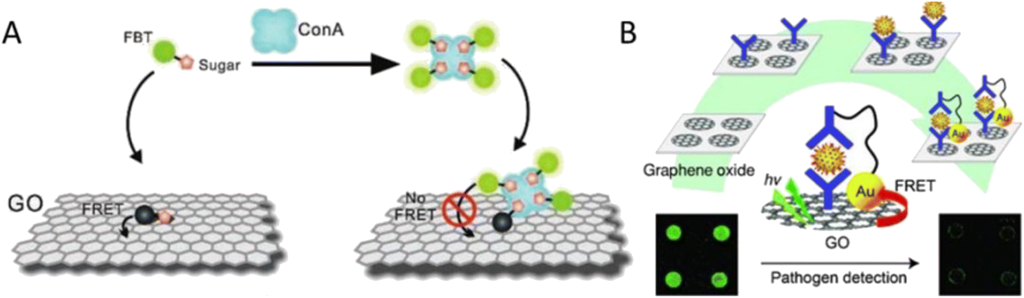 | ||
| Fig. 5 (A) The GO/FBT hybrid probe's ConA detection concept (Wang et al. 2011). Reproduced from ref. 58 with permission from John Wiley & Sons, copyright 2011. (B) Rotavirus immuno-biosensor system based on GO for pathogen model detection (Jung et al. 2010). Reproduced from ref. 59 with permission from John Wiley & Sons, copyright 2010. | ||
Additionally, it is water soluble and possesses a sizable functionalization platform, enabling the administration of many medicines. Because of its distinctive red/near-IR emission and dependency on pH for emission, GO has been successfully used to distinguish between acidic extracellular malignant environments of HeLa and MCF-7 (apo-transferrin on two cancer cell lines) cells.60 In fact, this strategy, along with further variation in the types of functional groups, GO flake size, and degree of oxidation, can enable this multifunctional imaging/sensing platform to be tailored to a variety of applications, such as the detection of enzymatic reactions, the detection of glucose or DNA, and microscopic optical pH sensing.
A typical enzyme found in 85% of cancers is telomerase. Single-stranded DNA (ssDNA) probes were connected to the surface of the quantum dots in order to demonstrate how the fluorescence of graphene oxide quantum dots (GOQD) changes in response to their interaction with telomerase as a diagnostic for cancer. The extension of the telomere-like probe on the surface of the quantum dots is what causes the considerable shift in emission wavelength of the fluorescence61 released by GOQD-DNA under UV illumination. In vitro bioimaging using decorated GO coated with polyethylene glycol (PEG) has received more attention recently as a luminous probe. Two-photon luminescence imaging of intravenously administered GO-PEG nanoparticles into mouse bodies via the tail vein reveals distinctive flow patterns of GO-PEG.62
4.1.2.4 Challenges and outlook. When using rGO in sensors, coverage experiments must be considered in order to calculate the precise amount of rGO that is needed. In addition, reporting the number of layers of rGO is crucial for direct comparison and field repeatability. The optimization and functionalization of the nanoparticles are crucial critical elements in the use of rGO/GO in the field of tribology to provide a stable and homogeneous solution. Therefore, for a more thorough investigation and characterization of rGO/GO, the long-term stability and functioning mechanism of nano-additives is still required.
The multifunctional properties of these new 2D materials motivate further investigation and, ideally, aid in overcoming the limitations imposed on them by their application in nanodevices. More experimental investigations in the mass manufacture of pure, defect-free 2D materials at an affordable price with an appropriate bandgap should be conducted at this stage of research. Building device prototypes in this situation could benefit from robust theoretical hypotheses derived from numerous DFT simulations of 2D materials with suitable electrical composites. It is now necessary to explore novel heterostructures besides graphene in order to create faster, more compact, and intelligent nanoelectronic devices that the upcoming generation will need.
Silicene62 is a newly discovered 2D material that, like graphene, is expected to show Dirac physics but with stronger spin–orbit interaction (SOC). The spin–orbit interaction is fairly strong in silicone and finally results in a tiny bandgap (∼1.55 meV) opening near the Dirac point. The form of silicene with the lowest energy, which has the top and bottom Si atoms spaced vertically by around 0.44 Å, is predicted to show a tiny amount of buckling. The inversion symmetry of the system is projected to be broken by the application of an electric field perpendicular to the plane because it will cause charge transfer between the top and bottom Si atoms, opening an energy gap.
Zhao et al. described the recent experimental accomplishments of silicene and its diverse prospective uses in nanoelectronics.62,63 Chowdhury and Jana then gave a thorough evaluation of theoretical studies on silicene.62 Germanene, the germanium equivalent of graphene, does not have a bandgap, but when a vertical electric field is applied, it may be employed in the channel of high-performance FETs. We attempt to highlight some significant studies on silicene and germanene in the section that follows. There is also a thorough discussion in the section on the optical and magnetic characteristics of FS silicene and germanene.64
4.1.3.1 Synthesis and structural properties of silicene and germanene. Unlike graphene, which may also exist in FS form, silicene has only been produced on metal surfaces (in general). On conductive ceramic ZrB2(0001),65 an iridium (Ir) (111) substrate,66 and an Ag (111) substrate, silicene has been effectively produced.67–70 To test the stability and bonding of the monolayer, first-principles DFT simulations have been used71 to examine the electronic characteristics of a silicene monolayer on a variety of (111) semiconducting substrates, including AlAs, AlP, GaAs, GaP, ZnS, and ZnSe. With the exception of GaP, the top layer of a non-metallic substrate is subjected to p-type doping, whereas the metal substrate is subjected to n-type doping (111).
Germanene72 is a substance composed of a single layer of germanium atoms, which is formed on a substrate like Au (111)73 under conditions of extreme vacuum and heat. Al (111), Ag (111), Cu (111), and Sb (111) are just a few of the other metallic substrate surfaces that have undergone successful attempts at deposition using germanium molecular beam epitaxy (MBE) in addition to Au (111).74 Through first-principles research that looked at the feasibility of epitaxial germanene on a semiconducting gallium arsenide (GaAs (0001)) substrate, its high-quality thin films offer unique electronic characteristics suited to semiconductor device applications.30
4.1.3.2 Electronic properties of silicene and germanene. The primary distinction between graphene and silicene is that, in contrast to planar graphene, planar silicene is unstable. In contrast to graphene, silicon allows for the tuning of the bandgap with the application of a transverse external electric field. In contrast to the typical nonrelativistic system frequently seen in a condensed matter system, we now have another bench-top relativistic quantum system prototype in addition to graphene.
The Fermi velocity of electrons in silicene is about equal to or one order of magnitude less than that of graphene (∼106 m s−1), according to angle resolved photoemission spectroscopy (ARPES), which is frequently used to analyse the distribution of electrons in reciprocal space. In contrast to graphene, silicene exhibits a more pronounced spin–orbit interaction, which finally results in a tiny bandgap (∼1.55 meV) opening near the Dirac point.75 In other words, although Dirac fermions are substantial in silicene, they are massless in graphene. It should be noted that, while it contributes to the formation of a new area of study regarding the phenomenon of the quantum spin Hall effect (QSHE), this bandgap value is far from that needed from the point of view of current device applications.
Due to its mixed sp2–sp3 hybridized structure, buckling also plays a significant role in the structural stability of germanene. Additionally, Nijamudheen et al. discovered that buckled germanene is more stable than planar germanene, in contrast to graphene.76 Similar to graphene, germanene shows Dirac-cone-like characteristics and, in its free-standing (FS) form, has semimetallic properties.77 Germanene has stronger surface reactivity than graphene or silicene because its buckling is higher (Table 1). Due to its buckled shape, germanene has a far easier time opening its bandgap when an electric field is applied vertically or when its sub-lattice symmetry is broken.
| Parameter | Graphene | Silicene | Germanene |
|---|---|---|---|
| Lattice constants a (Å) | 2.468 | 3.858 | 4.06 |
| Bond length (Å) | 1.424 | 2.232 | 2.342 |
| Buckling Δ0 (Å) | 0 | 0.42–0.45 | 0.69 |
| Parameter (Å) | 2.8 | 1.6 | 1.3 |
| Hopping integral t (eV) | 0.02 | 1.9 | 3.3 |
| Energy, Eg (meV) | 1.01 | 0.65 | 0.62 |
| Fermi velocity, vt (106 ms−1) | 0 | 0.001 | 0.007 |
| Effective electron mass m* (m0) | 0.001 | 3.9 | 43 |
| λso (meV) | 0.00 | 0.7 | 10.7 |
| Rashba interaction (meV) ΔE(eV) | 8.7 | 7.2 | 8.1 |
However, compared to graphene or silicene, the SOC value of this material is relatively high (Table 1). By including appropriate defects, such as the inclusion of adatoms, the creation of vacancies, or strain engineering, it is possible to open the bandgap at the Dirac K point for germanene in a much more practical manner than for graphene or silicene. The Fermi velocity of germanene has been determined to be two thirds that of graphene. More intriguingly, germanene has a greater inherent carrier mobility than either graphene or silicene, which may be highly advantageous for using this material in nanoelectronic devices.
4.1.3.3 Functionalization of germanene and silicene. Adsorption or doping of impure materials or the introduction of a vacuum into a pure system are common techniques to modify electronic characteristics. Both doping and vacancy inclusion might be seen as flaws in immaculate layers. Pang et al. used DFT to examine the structural, electrical, and magnetic aspects of 3d transition metal (TM) atom adsorbed germanene layers.78 They said that semimetallic germanene may be converted into materials with properties resembling those of ferromagnetic half-metals, ferromagnetic metals, non-magnetic semiconductors, and even non-magnetic metals.
The atomic radii of As and Ga are similar to that of Ge. As a result, they can be naturally favored as n (As) and p (Ga) type doping components in germanene networks. This research79 has shown that, by selecting suitable doping elements, doping concentrations as well as doping sites, semimetallic germanene may be converted to semiconducting or metallic nature. Be-doped graphene will operate like a semiconductor with an indirect bandgap of ∼0.30 eV, according to the prediction of López-Urías et al.80 The electrical and optical characteristics of the Be-doped germanene system at various concentrations were investigated by Dhar and Jana81 in response to this aspiration. Calculations of the band structure show that the semimetallic properties of germanene persist at very low Be concentrations (3.12%). However, semimetallic germanene displays semiconducting properties at modest Be concentrations (from 6.25% to 15.62%). However, the germanene structure with the highest Be content (18.75%) has metallic characteristics. The configuration with the highest bandgap, ∼251 meV, among all semiconducting configurations, has a Be concentration of 15.62%. Germanene-based field effect transistor (FET) device designs may make use of this limited and sizeable bandgap.
According to Xia et al.,82 compared to the pristine layer, there are various noticeable variations in the DOS of N2, CO, CO2, H2O, NH3, NO, NO2, and O2 adsorbed germanene complexes. Additionally, Gürel et al. asserted that germanene can develop important functions by charging and the application of an external perpendicular electric field.83 Jamdagni et al.84 have studied the electronic characteristics of a few vacancy-induced fluorine (F), halogen (H), or oxygen (O) functionalized germanene complexes. In order to make germanene a viable material for device applications, it is therefore conceivable to change its electrical characteristics in a variety of ways. Additionally, Wang et al.85 studied the electronic characteristics of tiny organic molecules such acetone, acetonitrile, ammonia, benzene, methane, methanol, ethanol, and toluene adsorbed germanene complexes. They said that the bandgaps of these systems can be customized between 3.9 and 81.9 meV, which might be beneficial for making optoelectronic devices.
Semimetallic germanene has been shown to change into direct and indirect bandgap semiconductors by decoration with particular foreign elements (C, Si), and the bandgap values can be tuned from 26 meV to 287 meV, which may be used to create nanoelectronic tuning devices.86 Keep in mind that group IV elements like graphene and silicene are not magnetic by nature, and neither is bare or pristine germanene. Interestingly, a pronounced magnetic moment of magnitude 4.04 μB is noted for one of these C-decorated systems.
Zheng et al.87 applied first-principles computations to explore the electronic structure and magnetic characteristics of 2D hexagonal silicene adsorbed with H and Br atoms. They discovered that, while silicene that has been fully saturated displays nonmagnetic (NM) semiconducting behaviour, unsaturated silicene that has been only partially saturated with hydrogen or bromine exhibits localised and unpaired electrons that exhibit ferromagnetic (C) semiconducting or half-metallic behaviour, respectively.
Due to their proximity to C in the periodic table and the fact that doping significantly changes the electrical and optical characteristics of graphene, B and N are two obvious options as dopants. The electrical and vibrational characteristics of the doped system were investigated using an ab initio investigation of the atom adsorption and absorption of B, N, Al, and P atoms on silicene.88
The dielectric function ε (ω, k → 0) contains both a real and an imaginary part. The imaginary part always remains positive as a function of frequency (ω), while the real part changes sign from positive to negative and cuts the frequency (energy) axis. These unique frequencies corresponding to collective excitations of electrons are responsible for the emergence of peaks in the electron energy loss spectra (EELS). In contrast to graphene, no new electron energy loss spectra (EELS) peak appears in silicene nanosheets when substituted Al, P, and Al–P atom concentrations are varied for parallel polarization, according to research on optical characteristics.89 However, for perpendicular polarization, two small, reasonably significant, peaks appear for P doping due to buckling in the nanosheet. Using DFT, Chowdhury et al.90 investigated the influence of silicone nanodisk form on its magnetic and optical characteristics (addressed later). The overall number of atoms and the number of atoms in the edges are the only two factors that set these formations apart from one another, other than shape. The configuration with the largest magnetic moment (3.969 μB) among them is the zigzag triangular/trigonal (ZT) (N = 13, Ned = 9).
The interaction of silicene with various semiconducting dichalcogenide substrates, namely MoX2 (ref. 91 and 92) with X = S, Se, Te, has been significantly effective in controlling the electronic properties of these silicene heterolayer structures. For example, it has been demonstrated92 that, like FS silicene, silicene on MoTe2 is a gapless semiconductor.
4.1.3.4 Effect of strain on silicene and germanene. The band structures of graphene and other 2D hexagonal materials may be successfully modified by mechanical forces.93 According to Mohan et al.,94 6% uniaxial compression can result in a direct bandgap of 389 meV, whereas 6% bi-axial compression can result in an indirect bandgap of 379 meV. Instead of bond length, the mechanical flexibility of silicene can be explained by changes in bond angle. In reality, flexible nanoelectronics may benefit from the better mechanical flexibility of silicene compared to that of graphene.
Another well-known silicene derivative, silicane, transitions from a semiconductor to a metal under uniform mild strain and from an indirect to direct gap transition under large strain.95 It has been predicted96 from first-principles calculations on the changes in band structure caused by stresses that silicene and germanene both exhibit strain-induced self-doping behaviour in the Dirac-like electronic structures. This method of doping, in contrast to doping in graphene, does not need adsorbed atoms or molecules in the nanosheets and the distance between the Dirac point and the Fermi level may be controlled by the amplitude of the strain. DFT calculations by Liu et al.97 indicated that silicene retains its semimetallic character up to 7.5% tensile strain but beyond this strain, silicene transforms into a metal. DFT + Green's function and (screened) Coulomb interaction (GW) (many bodies study) formalism has been employed96 to study the electronic and optical properties of silicane under uniform biaxial tensile strain.
4.1.3.5 Challenges and outlook. In contrast to graphene, silicene cannot develop in FS form; hence a suitable single-metal substrate is needed for its formation. Moreover, research on experimental findings related to electronic band structures and DOS will be influenced by theoretical study using a variety of substrates. In this situation, integration of a silicene nanoscale device on a silicon platform may be accomplished by growing silicene with good lattice matching on huge silicon wafers via buffer layers.
It naturally follows that substantial advances in the methods for synthesising hetero bilayers or multilayers of silicene will serve as a baseline for examining their enormous potential for the creation of next-generation nanoelectronic devices. It is vital to investigate various adjustments to their electronic band structure and optical characteristics when stresses, doping, and defects are present. Like other group IV elements such as graphene and silicene, bare germanene has non-magnetic characteristics. However, by adding the appropriate foreign elements, it is feasible to produce magnetism in germanene, leading to spintronic applications.
Recently, Hussain et al.98 investigated the application of defective germanene nanosheets as sensors for harmful gases such as hydrogen sulfide (H2S) and sulfur dioxide (SO2). For future research, it could be interesting to investigate the impact of various defect types on germanene nanoribbons or nanodisks. It will also be intriguing to examine the consequences of the introduction of impurities into a hybrid structure made of germanene and other 2D materials (such as graphene or silicene).
For the use of a 2-D material in electronics devices, a finite bandgap opening is required. It should be noted that bandgaps of the order of 400 meV are needed for ordinary FET devices. As a result, a search is required to find an appropriate bandgap in defective and adatom-decorated germanene using the interaction between SOC and substrate. From an experimental perspective, regulated nano-engineering of germanene flaws may result in the fabrication of innovative and intelligent nanodevices in the future.
Recently, transport properties along with thermoelectric features of silicene and its appropriate derivatives have been reviewed.99 Most importantly, biosensing applications regarding DNA sequencing and detection of drugs can be noted from the changes in electronic structure or current–voltage characteristics.
4.2 Hexagonal boron nitride (h-BN)
Geim and Novoselov from Manchester University used the scientific idea of the thermodynamic instability of 2D materials, which had been foreseen by Landau and Peierls. Since the successful exfoliation of graphene from graphite using the Scotch-tape method in 2004, interest has shifted to graphene and 2D materials because of their distinctive features in contrast to those of their bulk counterparts. Hexagonal boron nitride (h-BN), a promising substitute for graphene, has been investigated in a variety of applications, including electrocatalysts, hydrogen storage, field emitters, and polymer matrix composites. This is due to its exceptional adsorption performance, high thermal conductivity, and desirable mechanical strength.100–102 In comparison to h-BN, boron nitride nanosheets (BNNSs) often display improved performance and more useful applications.103,104 Due to the partial ionic bonding (also known as lip–lip interactions) between adjacent B–N layers, the extraction of BNNSs from their bulk structures is far more difficult than it is for graphene.105 Even though there have been many attempts to acquire BNNSs, effective exfoliation of BNNSs still requires a lot of work.In most CVD methods, the synthesis of h-BN grown on a substrate occurs. In 1995, monolayered “white graphene” h-BN nanosheets were formed on the surfaces of Ni, Pd, Ru, or Pt.109 In 2002 the CVD technique utilizing B and MgO made a breakthrough in the scalable production of h-BN nanotubes.110 Cu and Ni films were used as substrates to create BNNSs with enormous lateral dimensions. By using plasma-assisted CVD, h-BN nanotube arrays were also produced on substrates.111 Prior to heating, extremely disordered structures created by pre-treating boron and nitrogen precursors in a ball mill chamber helped to start the formation of h-BN nanotubes.112 With the use of floating catalyst technology, the CVD process may be scaled up even further.113 In addition, “extended VLS growth” was invoked to prepare BN nanotubes using metal boride particles serving as both catalysts for nitridation and an in situ reservoir of boron components114,115 and ZrB2 particles.116 Not only can VLS pathways benefit from laser-assisted ablation and vaporization of BN raw materials,117 but direct growth without metal catalysts does as well.55 Liquid boron droplets may be used as the liquid component in a VLS-analog model for the direct growth process.118 The self-assembly of BN nanotubes was also accomplished without the need for a catalyst using a pressured vapour condenser method.119 Induction thermal plasma processing using h-BN, B, or BC4N with H2, N2, or H2–N2 has recently made it simple to produce scalable BN nanotubes at rates of 20–35 g h−1.120–122 In a highly polar solvent medium, such as N-methylpyrrolidone (NMP) or dimethylformamide (DMF), liquid-phase exfoliation of bulk BN may result in single or multilayered BNS. However, it is essential that the energy required to exfoliate BN must be akin to the solvent–BN interaction for peel-off to occur first followed by later scroll initiation.
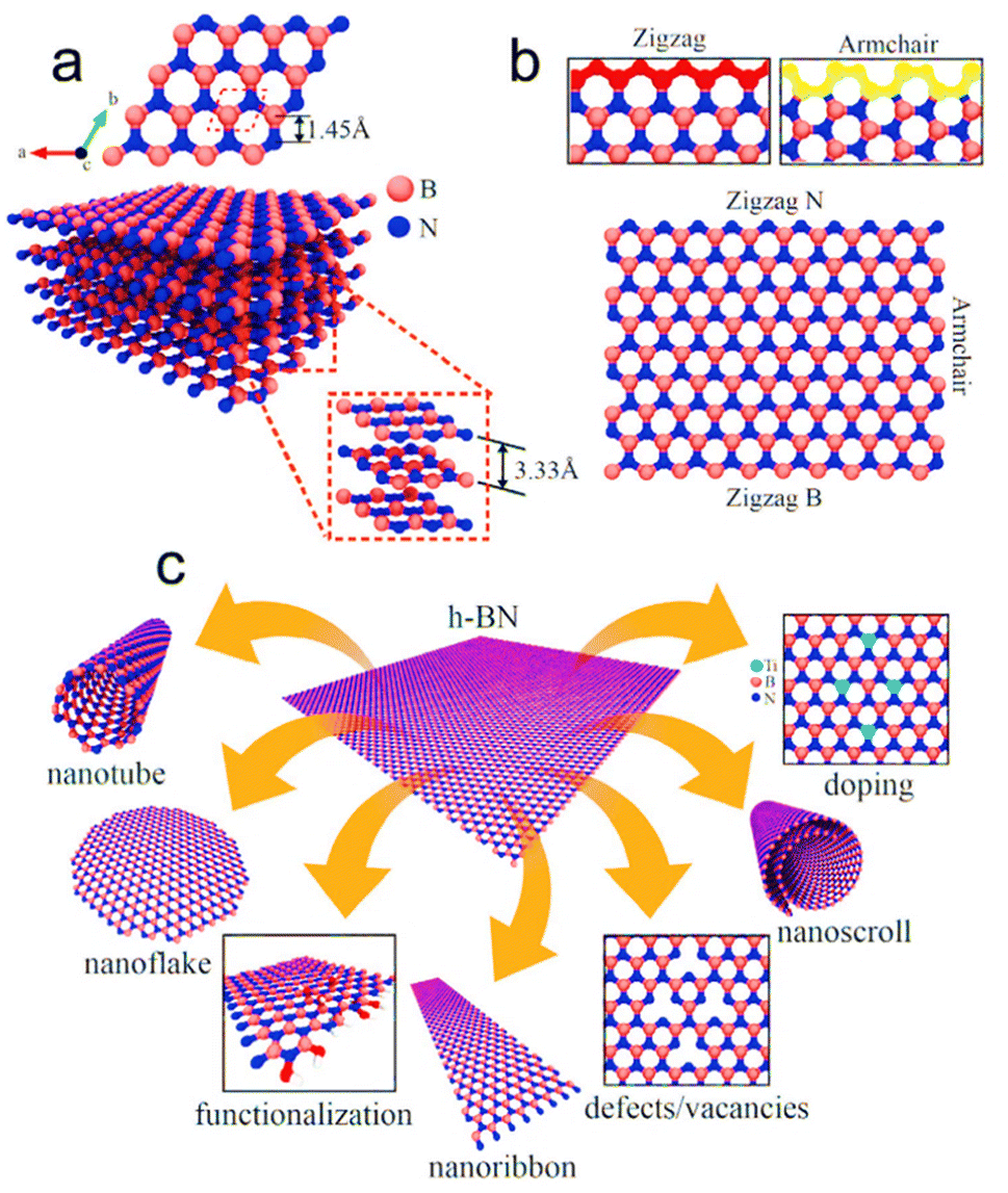 | ||
| Fig. 6 (a) Geometrical structure of h-BN; the unit cell is represented by red dashed lines. (b) Display of the probable atomic distribution of B and N atoms in different orientations. (c) Illustrations showing possible configurations that can be derived using h-BN. Reproduced from ref. 125 with permission from John Wiley and Sons, copyright 2021. | ||
Notably, 99% transparency is displayed by 2D h-BN nanosheets at wavelengths between 250 and 900 nm. Although a significant absorption peak may be seen in the deep ultraviolet (DUV) band (200–220 nm),125 optical absorption is rarely present. The optical bandgap of monolayer h-BN is found to be roughly 6.07 eV, in parallel with the theoretical calculations, in contrast to the bulk (bandgap 5.2–5.4 eV) (6.0 eV).126 Due to the interlayer-interaction-induced increase in electronic band dispersion, the value for the multilayer h-BN nanostructure is found to be in the range of 5.56 to 5.92 eV, which is lower than the theoretical calculation. h-BN nanosheets may show good possibilities for usage in ultraviolet lasing, photon emission, and DUV detectors due to their direct broad bandgap and ultraviolet luminescence properties. When the h-BN photodetector was lit in a dark environment, a high on/off ratio was in fact confirmed by increasing the current by three orders of magnitude.127
In an h-BN lattice, N atoms are expected to be replaced with O atoms, along with unpaired electrons and the accompanying paramagnetism. In fact, a strong EPR resonance signal with a predicted g-value of 2.0034 was found in a magnetic field of 320 mT.128 This shows that the synthetic BNO substance contains free electrons. By carefully adjusting the h-BN thickness, it is possible to improve the optical absorption of these spiral solar cell devices by up to 90% or the absorption relative to the quantity of photoactive materials utilized, resulting in an improvement of 762%.129 Similar to this, BNNSs are a good host for energy storage applications like hydrogen storage due to their increased surface to volume ratio.
Despite the fact that the theoretical prediction is around 600 W m−1 K−1, the actual experimental results (220–420 W m−1 K−1) have fallen far short of the forecast.123,131,132 The monoisotopic 10B and 11B h-BN in-plane thermal conductivities of 585 ± 80 W m−1 K−1 and 550 ± 75 W m−1 K−1 measured at 300 K, respectively, are stated to be the greatest room-temperature values for h-BN to date in the literature. The observed value of 408 ± 60 W m−1 K−1 for near-natural h-BN (78% 11B) is similar to the values previously reported by Sichel et al.123 and Jiang et al.131 for natural h-BN (80% 11B). Thermal conductivity is lowest for isotopically disordered h-BN, estimated at 330 ± 42 W m−1 K−1. The reported out-of-plane room-temperature (300 K) thermal conductivities (κz) for monoisotopic 10B, monoisotopic 11B, near-natural, and isotopically disordered h-BN crystals, respectively, are 3.5 ± 0.8, 4.5 ± 1.4, 3.3 ± 0.8, and 2.3 ± 0.5 W m−1 K−1. Fig. 7 provides a summary of the findings. All of these numbers are consistent with past natural h-BN reports in Jiang et al.131 and Simpson et al.132 The available literature serves as an example of how h-BN may be controlled to have high thermal conductivity, which opens up possibilities for the widespread use of h-BN as a next-generation thin-film material for thermal management, metamaterials, and metadevices.
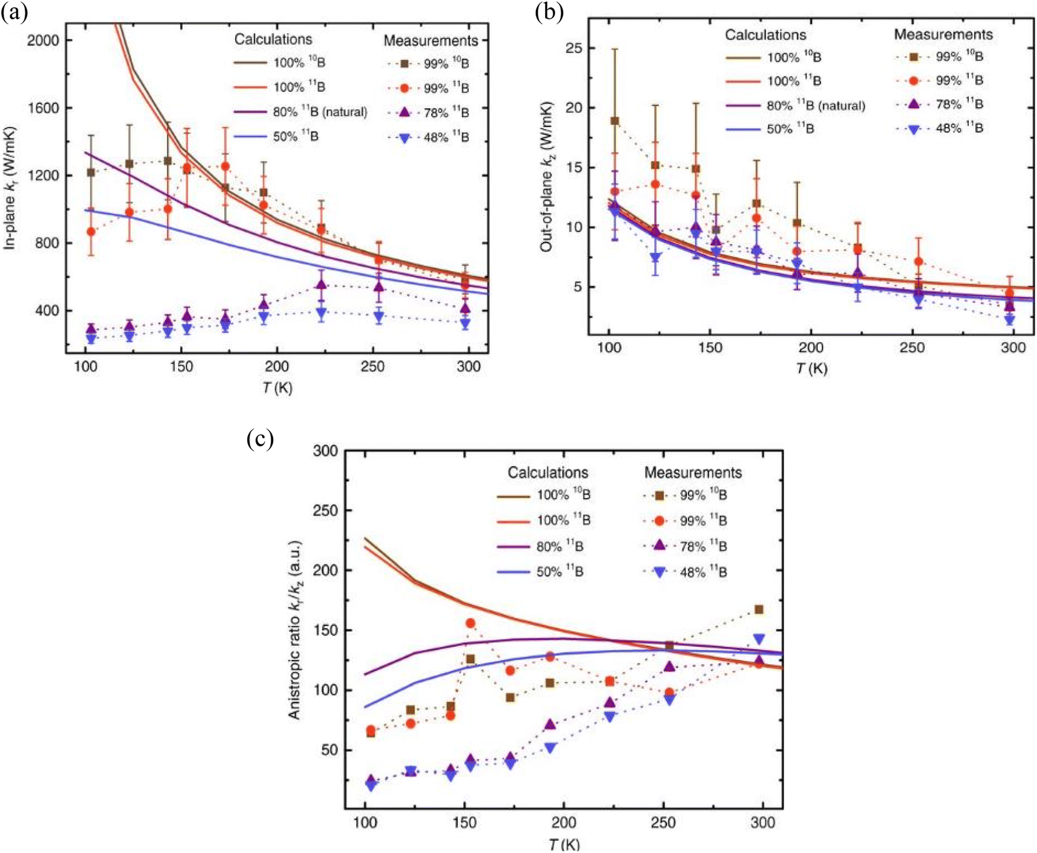 | ||
| Fig. 7 Temperature-dependent thermal conductivities and anisotropic ratios of hexagonal boron nitride (h-BN) crystals, as well as comparisons with model predictions: (a) in-plane thermal conductivity κr, (b) out-of-plane thermal conductivity κz, and (c) anisotropic ratio (κr/κz) for h-BN samples with variously tuned isotope ratios. Experimental data lines serve as eye-guiding markers. The findings of the measured thermal conductivity measurements are unclear, as indicated by the error bars in (a and b). Reproduced from ref. 133 with permission from Springer Nature, copyright 2019. | ||
Even more resistant than SiC, diamond, MgO, Mica, Si3N4, etc., monolayer h-BN has a Young's modulus predicted by DFT of 0.716 to 0.977 TPa (E2D = 279.2 N m−1).134 Although the defect density is quite high, the calculated Young's modulus values of CVD-produced h-BN films (2–5 layers) vary from 220 to 510 N m−1;135,136 while for 2D it decreased to 26.6 ± 1.7 N m−1 at 10% vacancies from 71.7 N m−1 for flawless h-BN. Thus it is evident that the decline in E2D values has a linear relationship with defect concentration and it is reduced to 1154 ± 14.8 N m−1 at 10% vacancies. Films 1 nm thick are estimated to have a breaking strength of 8.8 N m−1, breaking at deflections of 70 nm and stresses of around 221 nN. It was investigated whether the lower breaking stress and reduced stiffness are caused by defect presence or compliance at the margins.135,137 Once more, the Young's modulus was 0.865 TPa for tape-exfoliated h-BN monolayers with reduced defect densities. According to Cartamil-Bueno et al.,138 CVD-generated suspended monolayer h-BN has a tension and Young's modulus of 48 × 10−3 N m−1 and 936 GPa, respectively, under static mechanical testing.
Young's modulus is dependent on the thickness of h-BN, just like it is with faults. For a load of 2400 N m and 0.35% strain and 37 GPa of stress, an elastic modulus of 18000 N m−1, equivalent to a Young's modulus of 1.16 ± 0.1 TPa, is recorded.139 Overall, the mechanical characteristics of h-BN are promising enough for it to be used in the creation of multifunctional fillers for nanocomposites and nanomechanical resonators.140
Due to the widespread use of polymers as structure-reinforcing nanofillers, h-BN has demonstrated improved performance in nanocomposites because of its superior mechanical characteristics and highly anisotropic heat conductivity. Numerous studies published over the last several decades contend that polymer nanocomposites often improve performance even when reinforced by a low loading of nanofillers. For instance, Zhi et al.144 reported that the elastic modulus and strength of polymethyl methacrylate (PMMA) were increased by 22% and 11%, respectively, when just 0.3% of BNNSs was used. As a result of the effective interaction of the matrix with the embedded BNNSs, the coefficient of thermal expansion of PMMA also noticeably decreases. Again, h-BN has been used as a filler in other polymer matrices such as PVA,145 polyurethane (TPU),146 rubber,147 and epoxy148 to increase both the mechanical and the thermal properties.
Since h-BN is an isoelectric analogue of graphite, it has been extensively commercialized for use as Li-ion battery anodes in electrochemical energy storage applications. On the other hand, the qualities and mechanical toughness of h-insulating BN are extremely desirable for energy storage methods since they may be used as an electrode additive or as a separator. However, the usage of h-BN in supercapacitors and rechargeable lithium battery systems has been spurred by straightforward functionalization, structural modification, and incorporation into composites.
The fascinating optical properties of h-BN have encouraged its use in a multitude of applications.149,150 It has strong potential for nanophotonics because of its natural hyperbolic phonon–polariton modes151,152 and crystallographic defects.153,154 Grosso et al.155 demonstrate high single-photon count rates exceeding 7 × 10⁶ counts per second at saturation using strain control of the emission wavelength. A sharp reduction in broad and bright autofluorescence of the as-prepared h-BN samples is observed for targeted ion beam and high-temperature annealing. Similarly, strain-controlled optical characteristics of SPE h-BN have been demonstrated.156
Numerous uses for h-BN have been made possible by its intriguing optical characteristics.149,150 Due to its inherent hyperbolic phonon–polariton modes151,152 and crystallographic flaws, it offers significant promise for nanophotonics.153,154 Using strain control of the emission wavelength, Grosso et al.155 establish high single-photon count rates surpassing 7 × 10⁶ counts per second at saturation. For focused ion beam and high-temperature annealing, a dramatic decrease in wide and strong autofluorescence of the as-prepared h-BN samples is seen. Similarly, SPE h-BN has shown strain-controlled optical properties.156
H2 is an intriguing renewable energy source, but producing and storing it for use in real-world applications remains difficult tasks.157 Low-dimensional h-BN materials have been shown to have high H2 absorption capability due to partial H2 chemisorption and greater interactions with heteropolar B–N bonds.158,159 A one-step, template-free reaction was used to create highly porous h-BN microbelts, which created a material with a large specific surface area (1488 m2 g−1). Additionally, BN microbelts exhibit reversible H2 absorption from 1.6 to 2.3 wt% at 77 K and at relatively low pressure (1 MPa), according to an H2 sorption study.160
Innovative h-BN-based polymers have been specifically created for the purification of water. BNNSs are good candidates for the adsorption of contaminants, such as oil and organic solvents from heavy industries, enabling water treatment, because of their promising adsorption capabilities.161,162 For instance, utilizing a two-step atomic layer deposition (ALD) method, nanostructured BNNSs were created when borazine was deposited on polycarbonate and polyacrylonitrile membranes. For oil/water separation, the produced BNNSs are noteworthy due to their hydrophobic behaviour and strong lipophilicity.163 By combining ALD-mediated h-BN deposition on a carbon nanofiber template with annealing procedures at high temperature, Weber et al.'s team of researchers164 created BNNSs with adjustable properties. The acquired BNNSs showed admirable mechanical and adsorption capabilities (oil absorption up to 110 times their own weight in oil while resisting water) and are therefore extremely promising for depollution applications.
Additionally, h-BN nanocomposites can be utilized as drug delivery vehicles. Indeed, because of their stability, adaptability, changeable shape, low toxicity, and biodegradability, BNNSs are ranked as an excellent choice for a nanocarrier. It is possible to customize the shape of h-BN to produce the best possible drug loading and delivery.165 Studying the behaviour of doxorubicin hydrochloride (DOX), an anticancer medication, loaded on BN oxide nanosheets using density functional theory and molecular dynamics also shows great potential (BNONS).166 BNNSs show a lot of potential in this regime because of their unique characteristics, such as hierarchical porosity and high specific surface area. Various aspects of h-BN nanocomposites in the respective fields of application are presented in Fig. 8.
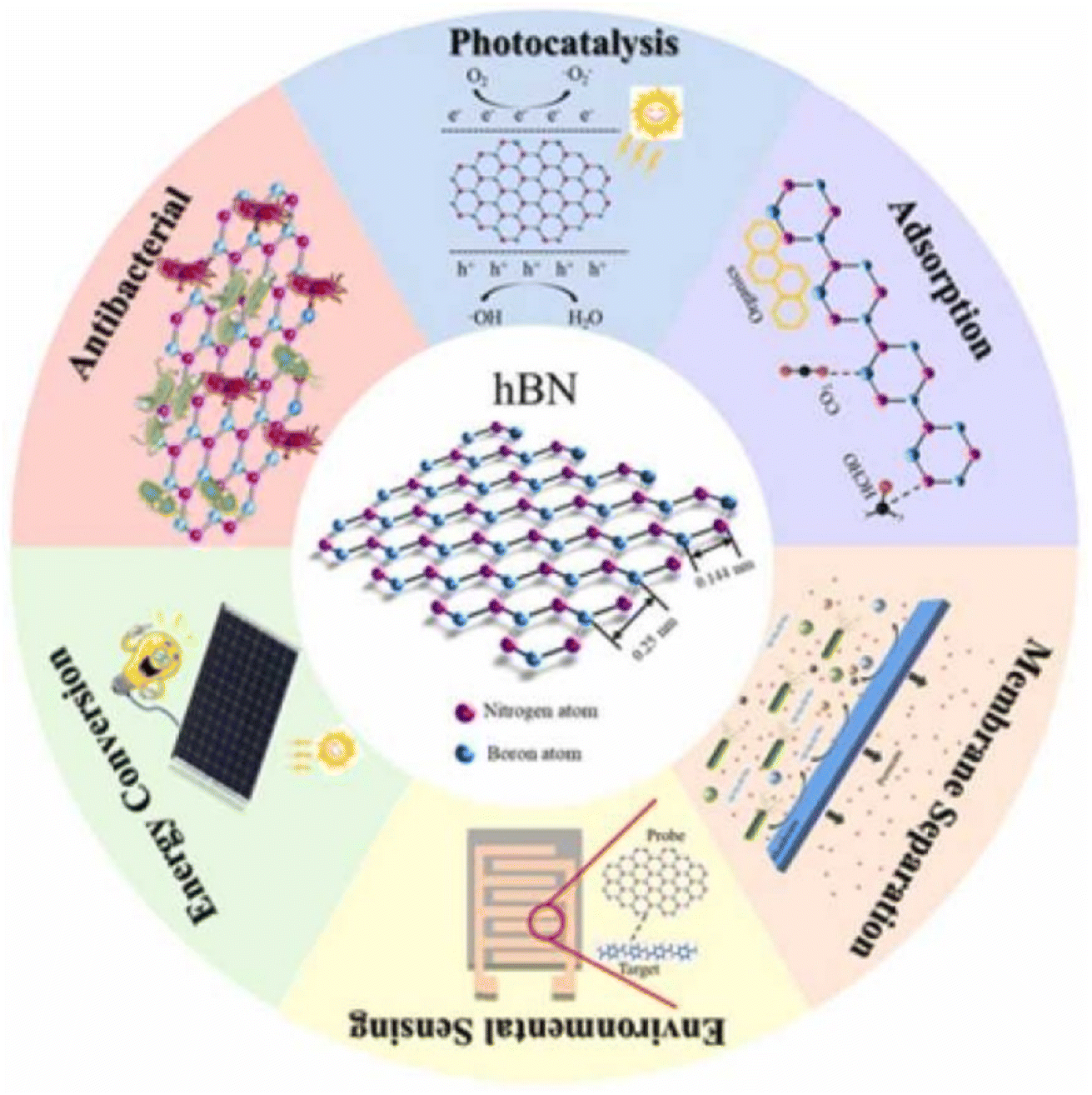 | ||
| Fig. 8 The various fields of application of h-BN nanocomposites in a nutshell. Reproduced from ref. 167 with permission from Elsevier, copyright 2022. | ||
By functionalizing h-BN with different doping elements and functional groups, their physical, chemical, and biological characteristics may be drastically altered. Because carbon and graphene are atomically similar, combining or integrating them might possibly alter the structure and functional properties of hBN. With tuneable mechanical, optical, and transport properties, many types of 2D heterostructures and hybridization based on graphene and h-BN nanosheets have been produced.
Again, h-BN has many distinct kinds of tiny vacancies that may be exploited as single-photon sources because of deep trap emission in the bandgap. Regarding the production of electronic devices, it is important to carefully evaluate the growth of flaws caused by sources of charge fluctuation via external energy.
4.3 Transition-metal dichalcogenides (TMDs)
Due to its zero bandgap and poor spin–orbit interaction, the remarkable potential of graphene cannot be realized technologically.33,168 As a result, the search for substitute materials with monolayer formation capability has given rise to a new field of research focused on lamellar transition-metal dichalcogenide (TMD) materials.The family of materials known as TMDs, which consists of a transition-metal layer sandwiched between two densely packed chalcogenide (S, Se, Te) planes, has a variety of intriguing characteristics. It has the general formula MX2 where X is a chalcogen atom of the VI A group and M is a transition element (Mo, W, V, etc.). TMD research has a long and successful history. Linus Pauling originally identified their structure in 1923.169 About 40 of them were known to have 2D architecture by the late 1960s.4,5 Robert Frindt is credited with writing the initial papers on the manufacture of monolayer MoS2 using adhesive tape in 1963,170 and suspensions were first attained in 1986.171 Then after the discovery of graphene in 2004, research attention continued to be stimulated towards 2D layers due to their graphene–analogous properties that can be exploited in diverse fields.
4.3.1.1 Top-down methods.
4.3.1.1.1 Mechanical exfoliation. In the mechanical exfoliation procedure, layers are separated from the bulk crystal by mechanical force. Graphene, a graphite monolayer, is where this concept originally came into being.177 It is a straightforward, economical approach that works with all van der Waals materials. Furthermore, because it is produced directly from natural bulk crystals, a high-quality monolayer may be obtained.178 Scotch tape, ball milling, gel-assisted exfoliation, metal-assisted exfoliation, and layer-resolved splitting (LRS) techniques are a few of the different varieties.179–181
Novoselov et al.182 are credited with using the Scotch-tape approach to derive a TMD monolayer for the first time. By repeatedly folding and unfolding the tape, a bulk crystal of a 2D material that has been placed in the center of the tape becomes thinner. An appropriate substrate (often SiO2 or SiC) is then covered with the thinned 2D material layers/tape, and consistent pressure is applied to improve adhesion between the substrate and the thinned 2D material layers. Once the adhesive tape has been carefully removed, monolayers of 2D material will remain on the SiO2 substrate. This technique yields ultrathin 2D TMDs with very good crystallographic orientation and nearly defect-free large sizes, which are suitable for electrical devices and basic research.
4.3.1.1.2 Liquid-phase exfoliation. Since the Scotch-tape approach cannot be scaled up, researchers are working to close this gap using the liquid exfoliation method (Fig. 9). Furthermore, because the technique can be carried out at low temperature, 2D materials may be produced on a variety of substrates. The advantages of this technology are applicable to conductive electrodes, inkjet-printed electronics, thin-film transistors, and nanocomposites.183–186
 | ||
| Fig. 9 A schematic illustration of the liquid-phase exfoliation method.191 | ||
Through van der Waals contact, solvent molecules with the right surface energy bond to nanosheet surfaces. Therefore, the key to increasing the degree of exfoliation is to match the surface free energy of solvent molecules and nanosheets. Currently, organic solvents like N-methyl-pyrrolidone (NMP) and dimethylformamide (DMF) are the most common.187 Liquid exfoliation has so far been used to create a number of ultrathin 2D TMDs, including MoS2, WS2, NbSe2, TaSe2, and NiTe2.188
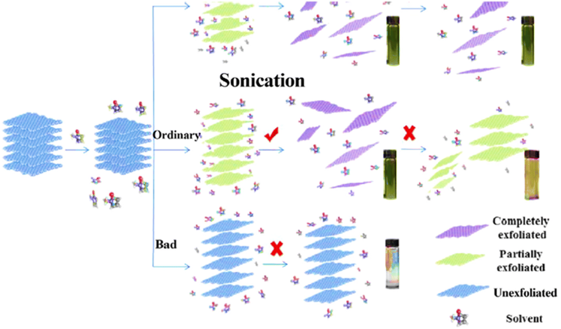
As an alternative, liquid exfoliation using ultrasonication in a particular solvent might provide effective separation of bulk crystals.189,190 The weak van der Waals interaction might be destroyed during the sonication process. As a result, by using the right ultrasonic duration and intensity, it is possible to exfoliate bulk crystals successfully.
4.3.1.1.3 Chemical exfoliation. Liquid-phase exfoliation using organic solvents is a scalable substitute for mechanical exfoliation and enables the production of flakes with adjustable thickness. A description of solutions containing single-layer MoS2 dates back to the 1980s,171 while the first report of liquid-phase exfoliation using Li intercalation was published in 1975.192 In-depth research is being done on new techniques for the liquid-phase exfoliation of TMDs employing Li intercalation.193,194 Exfoliation through Li intercalation has a number of drawbacks, including reported phase shifts from the semiconducting 2H to the metallic 1T phase194,195 and constrained sheet size. These findings show a relationship between the sheet size and significant in-plane resistance of the films.194
With the use of ultrasonication in water, the chemical exfoliation process inserts intercalators into the interlayer of the bulk crystals, resulting in the effective exfoliation of bulk crystals.196,197 Organometallic compounds, such as butyl lithium or naphthyl sodium, are the most typical intercalators. Intercalators are initially intercalated into the interlayer of bulk TMDs in water or ethanol during the synthesis process. The bulk TMDs are then sonicated into very thin nanosheets.198 Despite these achievements, TMD nanosheet wet chemical production is still in its infancy. The most difficult aspects of the synthesis are (a) finding and choosing the right metal and chalcogen reagents, (b) exercising strict control over metal oxidation states, (c) obtaining high purity and yield, and (d) comprehending how to truncate vertical development while allowing lateral expansion.199
The benefit of this method would be the possibility of functionalizing the TMD nanomaterial produced during the exfoliation procedure by adding additional dispersants or intercalants to the solution. Additionally, the final nanomaterial can be rendered water soluble depending on the kind of functionalization, enabling direct entry of these materials into biological systems.
4.3.1.2 Bottom-up methods.
4.3.1.2.1 Chemical vapor deposition. Chemical vapour deposition is the process that is used most frequently to create high-quality TMDs. The early descriptions of MoS2 synthesis relied on sulfurizing Mo that had already been placed on an appropriate substrate.4,101 Transition metal and chalcogenide atoms are provided via reaction precursors, which then react to generate 2D TMD films. The reaction product is then grown on the substrate, producing ultrathin 2D TMDs as a consequence.200,201 This method produces ultrathin 2D TMD nanosheets with outstanding electronic properties and high crystalline orientation. The existence of grain boundaries hinders the mobility of the films, according to research on the electrical transport of large-area devices made from comparable materials.202 The desire to regulate domain orientation led to further advances, such as the use of atomically smooth c-plane sapphire to facilitate the epitaxial CVD growth of monolayer MoS2.203
4.3.1.2.2 Solvothermal synthesis. Another innovation to the bottom-up approach is solvothermal synthesis. By using this technique, ultrathin 2D TMDs may be created from precursors with the help of a particular solvent and a certain reaction time.204 According to the literature, ultrathin MoS2 or WS2 nanosheets may be produced by reacting molybdic acid or tungstic acid with thiourea at 773 K for 3 hours. The advantage of this method is its ability to create ultrathin 2D TMDs in high yields at cheaper costs, which is promising for industrial applications.
4.3.1.2.3 Molecular-beam epitaxy. In order to fabricate semiconductor devices, molecular-beam epitaxy (MBE) has been used since the 1960s. An ultrahigh vacuum (UHV) is required for the deposition, which normally ranges between 10−8 and 10−12 torr.205 The molecular source for MBE for film growth is supplied from effusion cells by heating the solid material or supplying the gas source. No chemical reaction occurs during the production of source molecules, although one occurs on the target substrate.206 MBE may create a crisp, atomically thin layer between epitaxy layers or precisely dope the epitaxy layer by monitoring the shutters of individual effusion cells. UVH environments are also used in MBE to produce high-purity, defect-free films. Beginning in the 1980s, Koma synthesized monolayered MoSe2 on a CaF2(111) substrate.207 Since the doping of TMD can be achieved by introducing an extra molecular-beam source, MBE has the potential for fabricating a heterostructure with a doped layer. Fu et al. achieved such single-layered MoS2 grown on h-BN.208 In Fig. 10, a brief precis of the literature is presented in graphical format regarding the bottom-up synthesis of TMDs.
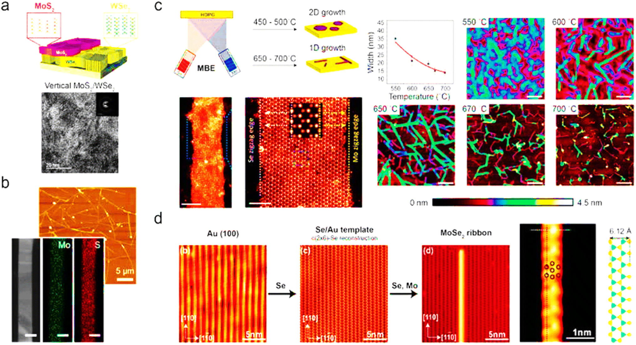 | ||
| Fig. 10 TMD nanowires and nanobelts made using bottom-up techniques. (a) Through the successive development of WSe2 and MoS2, vertically oriented MoS2/WSe2 heterostructures were created. (b) By-products of an atmospheric CVD process, such as MoS2 nanobelts. 100 nm scale bar. (c) During molecular beam epitaxy (MBE), the growth of MoSe2 nanoribbons whose widths may be adjusted by adjusting the substrate temperature. Scale bars: 5, 2, and 200 nm (from left to right) (panels to the right). (d) Ultrahigh vacuum (UHV) chamber-based growth of ultranarrow MoSe2 nanoribbons on Au (100) substrates with associated characterisation using high-resolution scanning tunnelling microscopy (STM) at 0.4 K. Reproduced from ref. 209 with permission from American Chemical Society, copyright 2020. | ||
4.3.2.1 Crystal and electronic band structure. TMDs are layered materials in which each unit (MX2) is made up of two atomic layers of chalcogen (X) sandwiched between a transition metal (M) layer. The structures of 2D TMDs may be divided into trigonal prismatic (hexagonal, 2H) and octahedral types depending on how the atoms are arranged (tetragonal, 1T).210 Each metal atom in a 2H-phase material forms two tetrahedrons with six branches in the +z and −z directions, whereas the top view reveals hexagonal symmetry (Fig. 11(a)). The chalcogen atoms in the T-phase are arranged hexagonally in the top view due to the trigonal chalcogen layer on top and a single layer with a 180° rotated structure (referred to as a trigonal antiprism) at the bottom.210
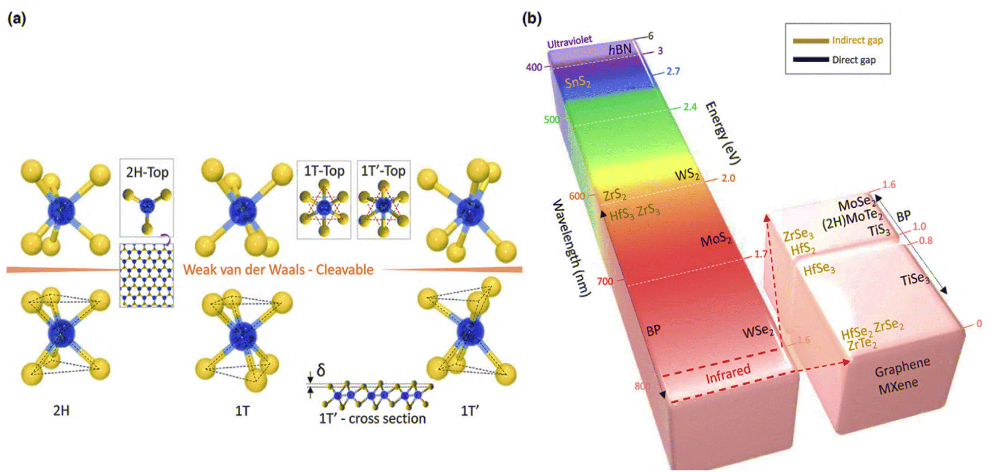 | ||
| Fig. 11 (a) Typical structures of layered transition metal dichalcogenides. Layered TMD architectures with cleavable 2H, 1T, and 1T′ are shown. (b) Bandgap of 2D layered materials ranging from the broad bandgap of h-BN to the zero bandgap of graphene (white colour). The colour of the column represents the associated wavelength of the bandgap; for instance, the bandgap for MoS2 (1.8 eV) is red, whereas the bandgap for WS2 (2.0 eV) is orange. SnS2, ZrS2, HfS3, ZrSe3, HfSe2, ZrSe2, and ZrTe2 are examples of indirect materials, while direct bandgap materials are shown on the right-hand side of the column (h-BN, WS2, MoS2, WSe2, MoSe2, 2H–MoTe2, TiS3 and TiSe3). Reproduced from ref. 210 with permission from Elsevier, copyright 2017. | ||
MX2 material possesses a stable 2H phase at ambient temperature, but a 1T phase may be produced by Li-intercalation211 or electron beam irradiation,212 depending on the precise arrangement of transition metals (group IV, V, VI, VII, IX, or X) and chalcogen (S, Se, or Te) components. A summary of the structure and bandgap variations of the complete class of TMD materials may be seen in Fig. 10.
Single-layer TMDs have direct bandgaps at the two inequivalent K and K′ points of the Brillouin zone (BZ) for the 2H structure. The dx2−y2 and dxy orbitals of the metal M, which combine with the px and py orbitals of the chalcogen X, are responsible for the crucial orbital character near the edge of the valence band. The edge of the conduction band, on the other hand, is created by the d3z2−r2 orbital of M, with assistance from the px and py orbitals of X. Multilayer compounds, as opposed to monolayer samples, are indirect gap semiconductors. The edge of the valence band lies at the Γ point of the BZ, with a major contribution from the d3z2−r2 and pz orbitals of the M and X atoms, respectively. It is noteworthy that the Q point is not a high-symmetry point of the BZ, for which the exact location depends on the layer number of the specific compound.
4.3.2.2 Optical and electronic properties. Compared to their bulk counterparts, single-layer TMDs have a straight bandgap with unique optical and electrical characteristics. The impact of lateral confinement on the optical and electrical characteristics of TMDs has been the subject of several studies. Bao et al. carried out subwavelength imaging of exciton recombination using a Campanile nano-optical probe of monolayer MoS2.213 According to their research, exciton quenching happens at about 150 nm from the edge of the layered MoS2 crystal, indicating that crystals of lower width would have comparable impacts on their PL.213 According to a recent study by Chowdhury et al., MoS2 nanoribbons with a width of less than 150 nm display PL at 660 nm, indicating a significant blue-shift in PL energy compared to 2D MoS2 crystals.209 In that report, far-field PL mapping displayed a monotonic increase in PL energy as a function of decreasing nanoribbon width.
With the right material, 2D TMDs reveal a wide range of bandgaps that spans the whole visible to infrared spectrum.214 With the exception of GaSe and ReS2, most semiconducting 2D TMDs exhibit a direct bandgap in their monolayer topologies as opposed to an indirect bandgap in bulk.215 As an illustration, monolayer dichalcogenides such as MoS2, MoSe2, (2H)–MoTe2, WS2, and WSe2, all exhibit direct bandgaps with energies between 1.8 and 1.5 eV, whereas bulk phases have indirect bandgaps with lower energy. The metallic phase and the semiconducting phase coexist in the majority of MX2 materials.216 Although Li-intercalation or electron beam irradiation can induce the 1T phase, the MX2 material has a stable 2H phase at room temperature.217 According to reports, the chemically exfoliated 1T MoS2 phase conducts electricity 107 times better than the semiconducting 2H phase.218 When it comes to WTe2, the 1T or 1T′ phase is more stable at room temperature than the 2H phase.219 Because of how close their cohesive energy differences are, the 2H and 1T0 phases of MoTe2 may readily be manipulated into one another.
Since most MX2 are devoid of dangling bonds, some of them exhibit high mobility, depending on the choice of a suitable substrate and metal contacts. For example, MoS2 gives a mobility of 700 cm2 V−1 s−1 on an SiO2/Si substrate with a scandium (Sc) contact and 33–151 cm2 V−1 s−1 on a BN/Si substrate (encapsulated) at room temperature.220
4.3.2.3 Mechanical properties. Besides being an excellent electrical transport material, the mechanical flexibility and toughness of TMDs are similar to graphene. An exceptionally high Young's modulus (Y) of ∼0.33 ± 0.07 TPa has been reported in suspended few-layered MoS2 nanosheets.221 Bertolazzi et al.222 reported high in-plane stiffness and E of ∼180 ± 60 N m−1 and ∼270 ± 100 GPa, respectively, for single-layered MoS2. The Young's modulus of monolayered MoS2 surpasses those of stainless steel (204 GPa) and graphene oxide (207 GPa), resulting from the absence of stacking faults and defect-free highly crystalline atomically thin TMDs.223
TMDs are comparable to graphene in terms of mechanical flexibility and hardness, in addition to being an outstanding electrical transport medium. In suspended few-layered MoS2 nanosheets, an extraordinarily high Young's modulus (Y) of ∼0.33 ± 0.07 TPa has been found.232 For single-layered MoS2, Bertolazzi et al.222 observed high in-plane stiffness and E of ∼180 ± 60 N m−1 and ∼270 ± 100 GPa, respectively. Due to the lack of stacking faults and the presence of defect-free highly crystalline atomically thin TMDs, monolayered MoS2 has a Young's modulus that is higher than that of graphene oxide (207 GPa) or stainless steel (204 GPa).223
Creating chemical bonds with chemical groups that will be functionalized on the TMD surface is known as covalent modification. The functional material that is implanted onto the TMD determines how these alterations are made. For use in biological applications, TMDs can be covalently or noncovalently linked to polymers233,234 or smaller organic molecules.234,235 Another kind of modification involves adding metallic nanoparticles to the TMD sheets in order to decorate them236,237 and improve the electrocatalytic activity or to act as contrast agents in imaging. The behaviour of the TMD in the altered environment varies depending on the changes to the TMD and the interaction with external chemical constituents, and biological applications rely on this.
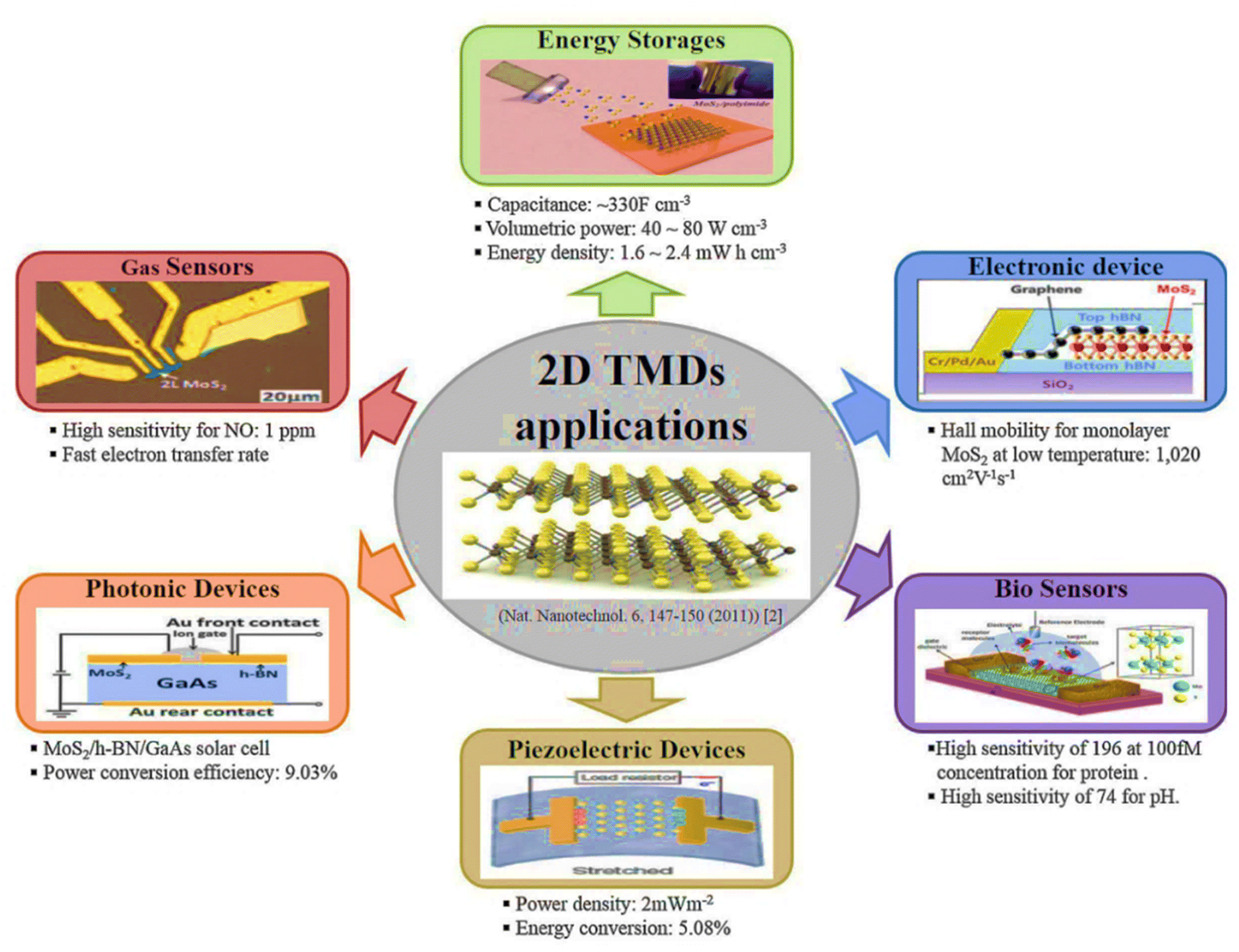 | ||
| Fig. 12 Electronic, optoelectronic and energy devices based on 2D TMDs. Reproduced from ref. 210 with permission from Elsevier, copyright 2017. | ||
4.3.4.1 Electrical and optoelectronics applications. High-performance 2D TFTs based on synthesized MoS2 have now been achieved after extensive research and development. These TFTs have the high on/off current ratio and current saturation that are typical of high-quality TMDs while they function at room temperature. The achievement of electron mobility of ∼50 cm2 V−1 s−1 and current density of ∼250 mA mm−1 in particular raises the bar for high-performance TFTs.210 Importantly, at a channel length of 0.5 mm and cut-off frequencies greater than 5 GHz have been attained on flexible plastic substrates.
Single-layered TMD crystals show substantial promise for use in innovative optoelectronics because of their varied exciton physics and broken in-plane inversion symmetry.238 Additionally, the substantial mechanical flexibility and electrical structural tunability of 2D TMDs support their incorporation into flexible and reconfigurable devices. 2D TMD photodetectors have high responsiveness and a low dark current, and they operate largely through the photovoltaic effect.239 Lopez-Sanchez et al.240 exhibited a single-layered MoS2 transistor with responsivity as high as 880 A W−1 when exposed to an electric field of ∼4 V μm−1.
In a significant piece of research, Mak et al. revealed the first 2D MoS2 transistor working in photoconduction mode, where photoexcited carriers improved the device conductance.241 It has been observed that single-layered WSe2 devices with electrostatically driven p–n junctions exhibit ambipolar transport properties.242,243 The photodetection responsiveness of WSe2 diodes irradiated with a 532 nm laser was demonstrated by Baugher et al. to be 210 mA W−1.242 Although these devices operate effectively at very high biases, their unoptimized device architecture and very low external quantum efficiency are a result of their low optical absorption.
4.3.4.2 Energy applications. Due to its stacked-sheet-like structure and enormous pseudo-capacitance brought on by its various Mo oxidation states (+2 to +6), MoS2 has demonstrated a high electrical double layer capacitance (EDLC). As a result, it qualifies as a potential 2D material for supercapacitor electrodes.244,245 Small sheet size, limited manufacturing yield, less uncontrollability in thickness, and flaws in the synthetic processes are potential issues related to its significant use.178,246
Supercapacitor electrodes made from chemically exfoliated MoS2 nanosheets showed remarkable capacitive performance, with capacitance values ranging from 400 to 700 F cm−3 in a number of aqueous electrolytes.247 Choudhary et al.248 described the direct manufacturing on flexible substrates (copper, polyimide) of a large-scale and distinctive 3D-porous MoS2 supercapacitor electrode. SiBs, or sodium-ion batteries, have lately been proposed as a replacement for lithium-ion batteries (LIBs). The materials for the graphite anode, however, cannot tolerate the huge size of Na+. Because of their roomy layered structures and good compatibility with host anode materials, TMDs like MoS2 and WS2 are the preferred materials.249
4.3.4.3 Gas sensors. Cho et al.250 actualized a gas sensing method based on charge transfer in atomically layered MoS2 employing in situ photoluminescence (PL). With the help of NH3 gas and NO2 (a p-type dopant), in situ PL spectra of MoS2 (n-type dopant) were captured. Using basic principles, Yue et al.251 calculated the adsorption energy and the quantity of charge transferred between monolayered MoS2 and several gas molecules, including O2, H2O, NH3, NO, NO2, and CO. The physical absorption of these gas molecules onto MoS2 with little charge transfer, acting to inject or withdraw electrons, was confirmed by DFT simulations.
Similar to MoS2, the number of layers and their alignment have a significant impact on the gas sensing capability of WS2. The relationship between the quantity of WS2 layers and sensing effectiveness was researched by Qin et al.252 The first demonstration of a single-layered MoSe2-based gas sensor device is credited to Late et al.253 Using electron beam lithography, monolayered MoSe2 isolated from bulk MoSe2 was created on a SiO2 substrate. Higher NH3 concentrations at room temperature increased the gas response of the MoSe2 sensor.254 Feng et al. researched gas sensors based on MoTe2, with encouraging outcomes.255
Due to their atomically layered structure, substantial surface area, and remarkable electrochemical properties when combined with surface functionality and electrical conductivity, TMDs have been suggested as potential candidates for high-efficiency energy storage. TMD materials are also thought to be one of the best options in the developing field of wearable electronics. The stretchability of TMDs should be further researched for stable operation in next-generation flexible technologies due to their wrinkled assembly.
Additionally, TMDs have generated interest as a new field of physics called “Valleytronics” due to their significant spin–orbit interactions and lack of inversion symmetry at their ultimate atomic thickness. New families of 2D materials, such as BP, silicone, and germanene, are expected to open the door to low-dimensional electronic/energy devices if their stability issues can be appropriately managed.
4.4 MXenes
With the general formula Mn+1XnTx (n = 1–4), MXenes are categorized as a large group of two-dimensional (2D) metal carbides and nitrides, where M stands for early transition metals, X is C/N, and Tx denotes the surface termination (i.e., hydroxyl, oxygen or fluorine that is produced due to immersion in an etchant).256,257 Since their discovery in 2011, MXenes have been the subject of extensive research due to their uncommon mechanical, electronic, and optical characteristics. In particular, sub-nanometer interlayer splits between 2D sheets in MXenes allow for quick ion intercalation and transport and are created by selectively etching, though they can be extended by combining heterostructure and appropriate 2D materials to create hybrids.258–261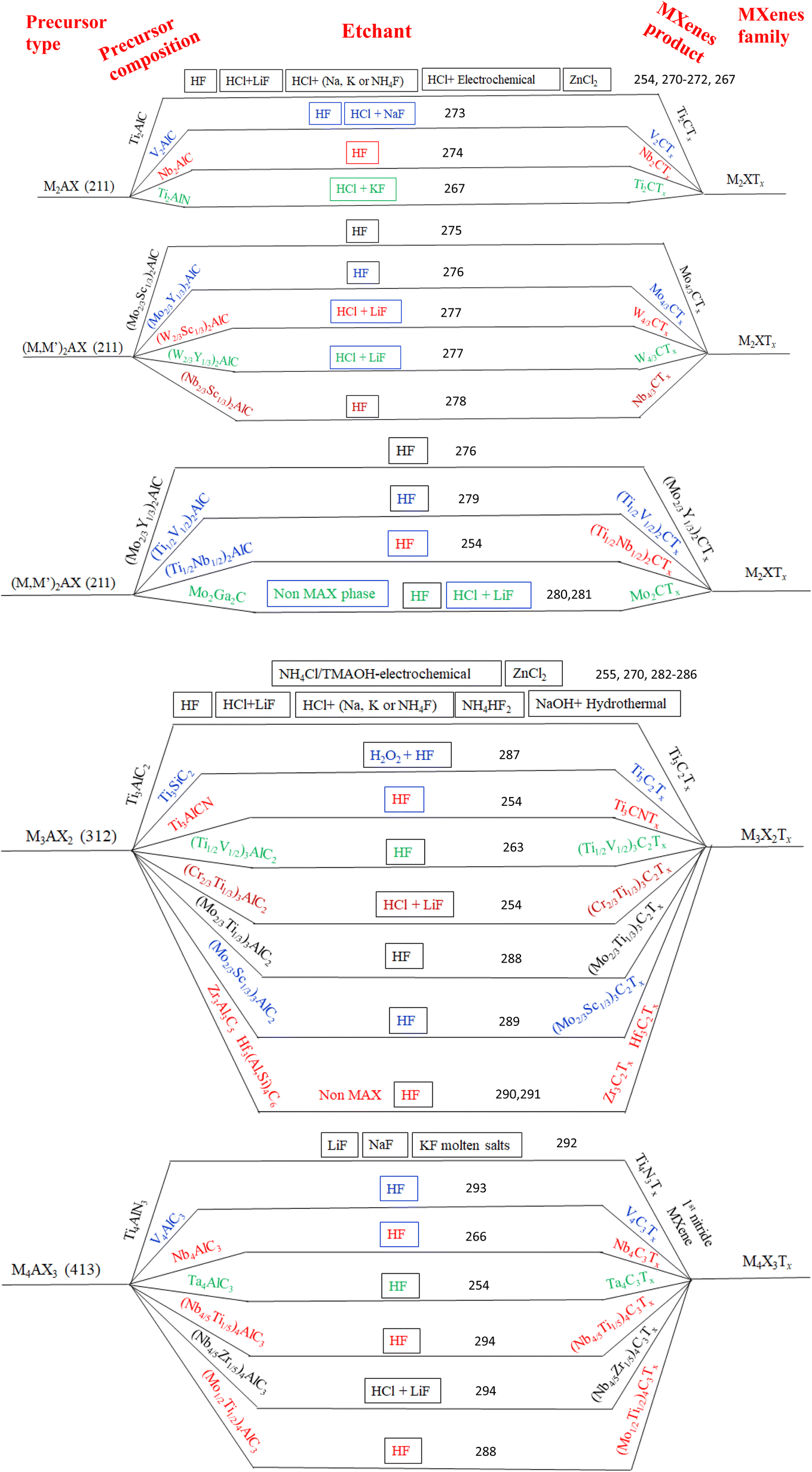 | ||
| Fig. 13 Existing MXene family with their precursors and etching route. | ||
:1 or 2:2 and 2:1, respectively. The ratios are produced by the different metal lattice sites in the MXene structures, and in the case of i-MXene, there is at least a 0.2-size difference between M and X.277,297 There are theoretically expected to be at least 26 different types of o-MXene, and some of them, M2AC2Tx (M = Mo, Cr, A = Ti, Sc), have already been synthesized.290,298 A honeycomb-like lattice is created by the hexagonal organization of the atoms in this structure, and the M atoms are located at the centers of the monoclinic (C2/c) or orthorhombic (C2/m or Cmcm) structures that make up the in-plane i-MXene.277 Ordered vacancies in i-MXene (W1.33CTx from (W2/3Sc1/3)2AlC) are produced as a consequence of the simultaneous HF etching of the A and M elements.279 The weak bonds between the M elements and carbon sites cause visible displacement from the M plane, and the characteristics of this structure allow for targeted etching of just the A or both the A and M from the i-MAX phase, i.e., Mo4/3Y2/3AlC.278
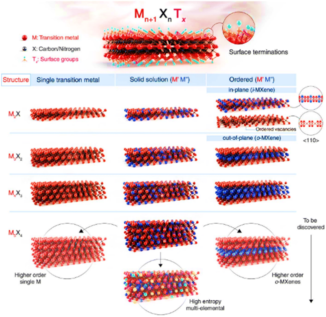 | ||
| Fig. 14 The general formula of 2D MXenes is Mn+1XnTx where M is an early transition metal, X is carbon and/or nitrogen, and Tx represents surface terminations of the outer metal layers. n can take values from 1 to 4, subject to the number of transition metal layers, i.e., Ti2CTx (n = 1), Ti3C2Tx (n = 2), Nb4C3Tx (n = 3), and (Mo, V)5C4Tx (n = 4). Reproduced from ref. 291 with permission from Elsevier, copyright 2017. | ||
The possibility of twinning in the M layers is made possible by the finding of a solid solution, which is composed of five M layers, Mo4VC4Tx, and differs from known MXenes. MXenes are classified as either solid solution or organized structure depending on whether one or more transition metal atoms are present in the M sites. For example, Mo2TiC2Tx is created by sandwiching two M layers together, and Mo2TiC3Tx is created by sandwiching one M layer between two M layers. One or three M layers could theoretically be squeezed between M layers (bottom row in Fig. 14), resulting in the formation of an M5X4 structure.299
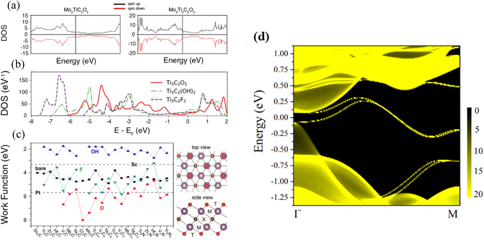 | ||
| Fig. 15 (a) TDOS of Mo2TiC2O2 and Mo2Ti2C2O2 indicates the effect of MXene structure. (b) DOS of Ti3C2, Ti3C2O2, Ti3C2(OH)2, and Ti3C2F2 show how the electronic properties of MXenes are affected by surface chemistry. Reproduced from ref. 314 and 321 with permission from John Wiley and Sons, copyright 2018. (c) The work function of various MXenes is dependent on surfactance. (d) Mo2HfC2O2 local DOS with energy and momentum dependence, where the edge states link the bulk valence and conduction bands at the M point by forming a single Dirac cone. | ||
In Fig. 15(c), where they are used as transparent conductive electrodes (TCEs) in OLEDs314 and photonic diodes, the work function (ϕ) of MXenes is highly tunable using an appropriate combination of transition metals, X elements, and surface termination.315 For instance, a Ti3C2Tx TCE in an OLED and the incorporation of a TiO2 electron transport layer in a perovskite solar cell improve the external quantum efficiency by 28.5% and 5%, respectively, over the original cell and the state-of-the-art commercial OLEDs.316 As the oxygen termination increases, OH always decreases, but F varies with the materials due to the influence of the surface dipole as compared to the naked surface.317 Fig. 15(c) shows the expected ultralow work function of hydroxyl (OH) surface terminated MXenes, which is attractive for emitter cathode field effect transistors (FETs). The lowest work function is 1.6 eV for Sc2C(OH)2. The work function is defined as the difference between the Fermi level and the vacuum level; shifting the Fermi level to a lower level has the effect of increasing the value of the work function. In general, the work functions for the O- and F-terminations show higher values than OH–. However, even compared to bare MXenes, where the negative surface dipole moment is actually operative, the value of the work function in the case of OH– is significantly lower.318 The controlling surface, which is extremely effective for the TCE, can be used to achieve a high value of 5.1 eV and large electrical conductivity of 11670 S cm−1.319 Ti3C2 is discovered to have a value of 4.60 eV, which makes it a better contact than ZnO or SnO to form n-type and p-type thin-film transistors, respectively.320
According to the definition of a topological insulator (TI), electrons with opposing spins propagate in opposite paths after low-dissipation electron transport. It is anticipated that the presence of heavy elements in 2D materials will result in TIs, in which spin–orbit coupling (SOC) has a significant impact on the electrical structure. As a result, MXenes containing strong 4D and 5D transition metals like Mo, W, Zr, or Hf may manifest as 2D TIs. It is expected that few MXenes will be TIs. 2D TI behavior has been found in MXenes double ordered transition metal carbides in M2MC2O2 (M = Mo, W and M = Ti, Zr, Hf) with O-termination.321,322 Fig. 15(d) shows an illustration of the energy–momentum local DOS of Mo2HfC2O2, where a Dirac cone is created by the edge states at the M point and attaches the bulk valence and conduction bands to safeguard the topological character. Recently, TI behavior has been revealed in a nitride-based MXene, Ti3N2F2. The TIs in MXenes have typically only been studied using complete O- or F-termination up until this point, and there has not been a comprehensive report on how surface termination affects the behavior of MXene TIs. Additionally, the behavior of MXenes is only anticipated; none of them has yet undergone experimental observation.323
| Solution | Film | λmax | |
|---|---|---|---|
| Ti2C | Wine | Green | 542 |
| Ti3C2 | Forest green | Dark purple | 800 |
| Nb2C | Blue hue | Yellow | 915 |
| Nb3C2 | Gray | Blue | No peak |
| V2C | Green-blue | Bronze | No peak |
| Mo2C | Brown | Green | 450 |
| Mo2TiC2 | Orange-brown | Light blue-silver | 476 |
| Mo2Ti2C3 | Grey | Dark green-grey | No peak |
| Ta4C3 | Brown | Sliver-grey | No peak |
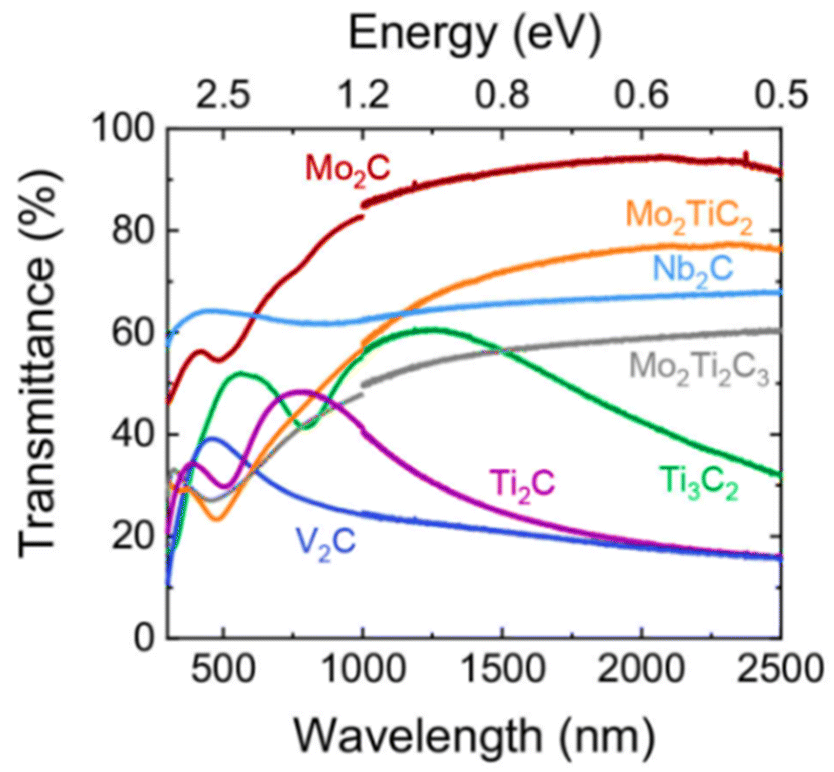 | ||
| Fig. 16 Transmittance profiles for various MXene materials. Adopted with consent from ref. 324. | ||
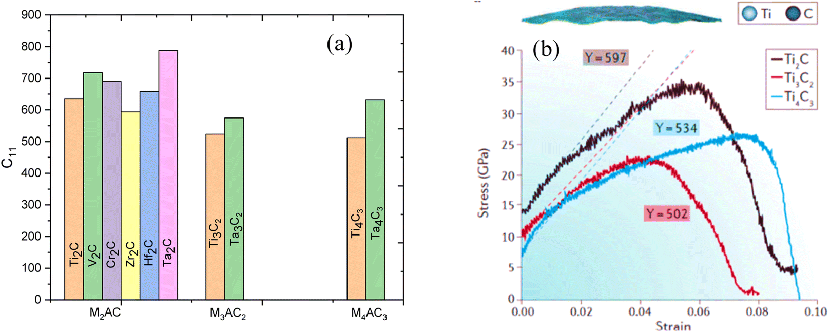 | ||
| Fig. 17 (a) Calculated elastic constant values for various MXenes. (b) MXene stress–strain curves for Ti2C, Ti3C2, Ti4C3. Reproduced from ref. 15 with permission from Springer Nature, copyright 2017. | ||
Fig. 18(a–h) show how the AFM nanoindentation experiments were explained in terms of the monolayer of Nb4C3Tx.328 It provides noncatastrophic fracture with a 202 nN maximal load. For monolayered Nb4C3Tx flakes, the typical 2D elastic modulus and pre-stress level are determined to be 486 to 18 N m−1 and 0.06 to 0.32 N m−1, respectively. A comparison of different 2D materials is shown in Fig. 18(i), where these materials exhibit greater values than those of Bi2Se3,329 InSe,330 WSe2,331 MoS2 (ref. 222) or WS2,332 but still fall short of those of graphene333 or h-BN.334 It is anticipated that nitride-based MXenes will have a greater in-plane Young's modulus than carbide-based MXenes.335
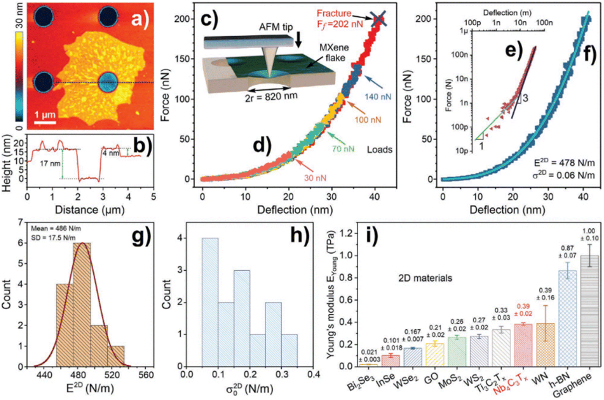 | ||
| Fig. 18 Nb4C3Tx indentation test findings for Nb4C3Tx: (a) AFM picture. (b) Measurement of the AFM height profile. (c) The tip of the ATM on the suspended membrane. (d) The force–deflection curve for various weights. (e) The loading curve for the Nb4C3Tx membrane. (f) The loading curve with least squares fit to the experimental data. (g) Distribution of elastic elasticity for 1L Nb4C3Tx membranes. (h) Pre-stress conditions for a monolayered membrane. (i) Comparative chart Young's modulus for various 2D materials. Reproduced from ref. 328 with permission from John Wiley and Sons, copyright 2020. | ||
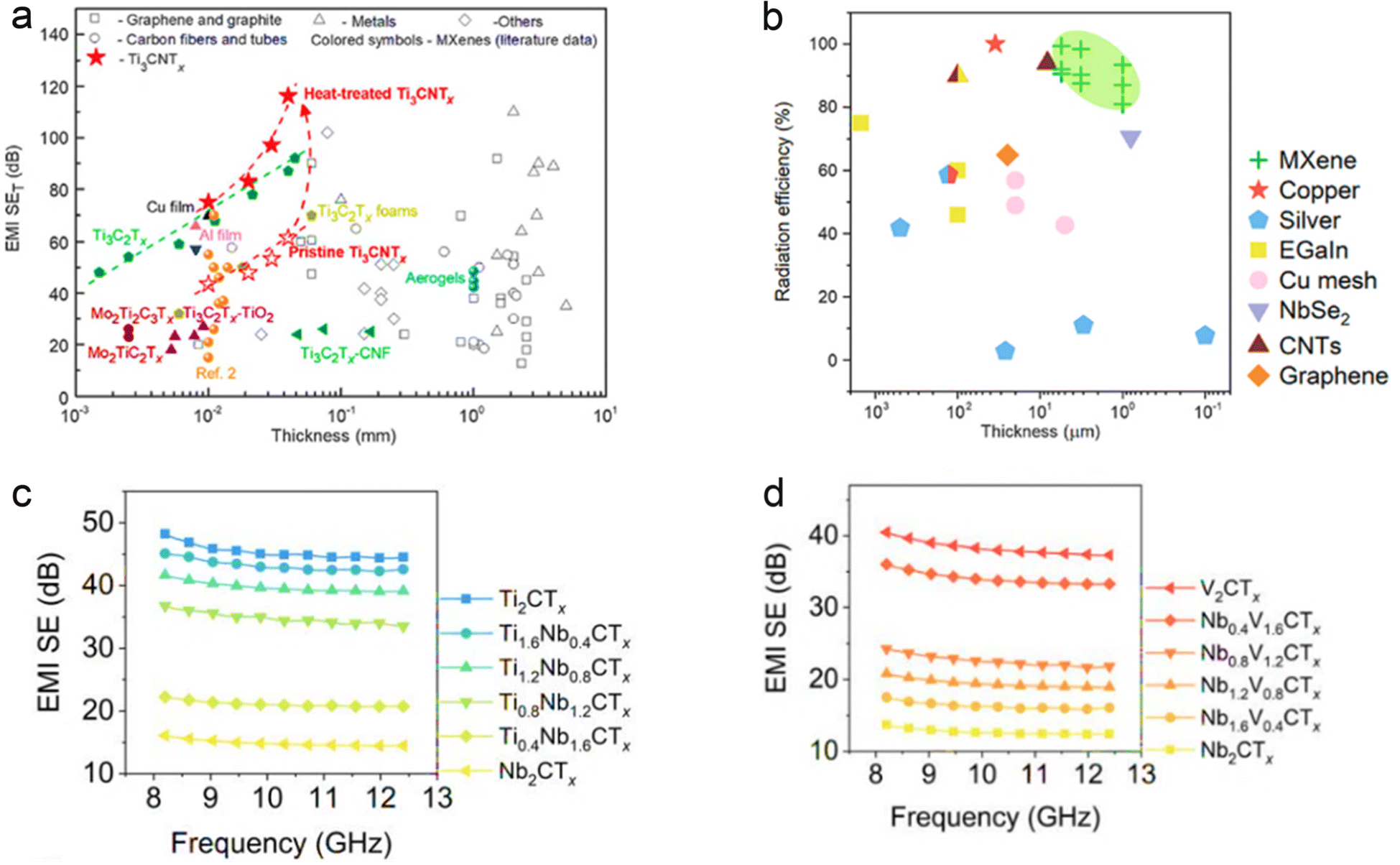 | ||
| Fig. 19 (a) Comparison of EMI shielding efficiencies of MXenes with carbons and metals. (b) A comparison of radiation efficiency versus thickness for MXene with metals, carbons, and others as patch antennas. (c and d) EMI SE of various MXenes with their solid solutions. Reproduced from ref. 337 with permission from [John Wiley and Sons], copyright [2020]. | ||
The EMI shielding efficiency of Ti-based MXene is greater than that of other MXene materials. Additionally, Fig. 19(c) and (d) illustrate the EMI shielding characteristics of some solid-solution MXenes, demonstrating how the chemical composition can be adjusted to alter this characteristic.338 Due to its increasing absorption, thermal annealing of Ti3CNTx results in a greater shielding efficiency than Ti3C2Tx.339 Fig. 19(d) illustrates a contrast in the annealing temperatures for Ti3CNTx and Ti3C2Tx. The value of total shielding efficiency of 40 m-thick Ti3CNTx is raised to 116 dB for an annealing temperature of 350 °C, indicating that the annealing temperature has a significant impact on EMI SI.
The samples are annealed at 800 °C for two hours in an argon environment in Fig. 20(a).340 The EMI SE value of the annealed sample is greater than those of clean 60 and 70 wt% samples but less than those of 80 and 90 wt% samples By foaming the porous structure, the EMI performance of 6 m-thick MXene can be raised to 70 dB from its initial value of 53 dB.341
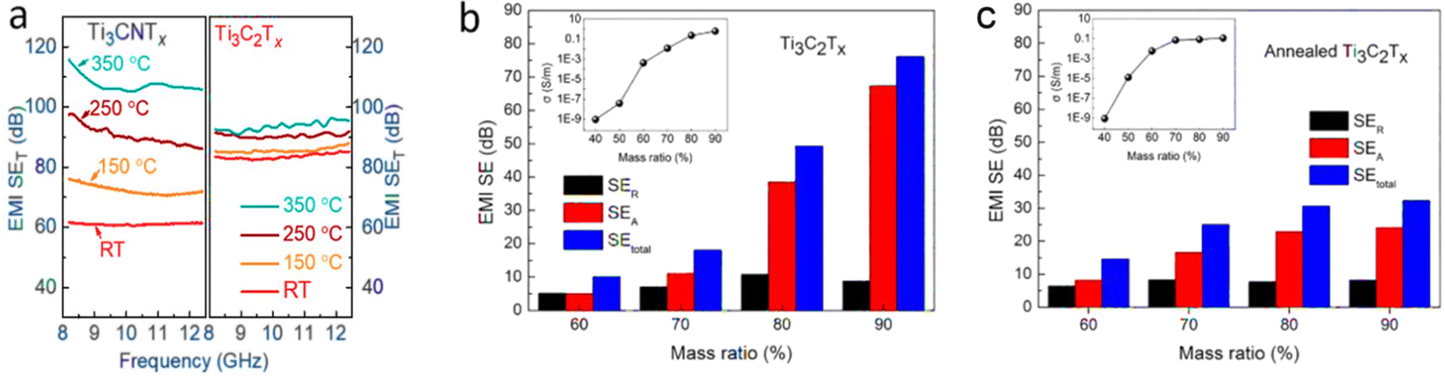 | ||
| Fig. 20 (a) comparison between Ti3CNTx and Ti3C2Tx with regard to annealing temperature. (b and c) Annealing effect for Ti3C2Tx/wax composites. Reproduced from ref. 340 with permission from American Chemical Society, copyright 2016. | ||
Replacing the Al layer reduces the interactions between MXene layers during the exfoliation synthesis technique. Therefore, surface termination is crucial in regulating the storage capability of MXenes. By blocking ion transport, termination by –F and –OH greatly reduces the capacity (from 320 for Ti3C2Li2 to 130 and 67 mA h g−1, respectively).343 However, by increasing Li mobility and lowering the diffusion barrier, which is lower than that of graphene, termination with chalcogen atoms (S and Se) increases the capacity.344 For non-lithium-ion batteries (NLiBs), MXenes can transport ions of various sizes in addition to Li-ions. Fig. 21 displays the storage capabilities of various ion batteries made of oxygen-terminated and bare MXenes. Due to their lighter weight, bare MXenes work better, and oxygen-terminated MXenes can break down into bare MXene. Additionally, adding a metal layer nearly doubles the ability for different ions.345
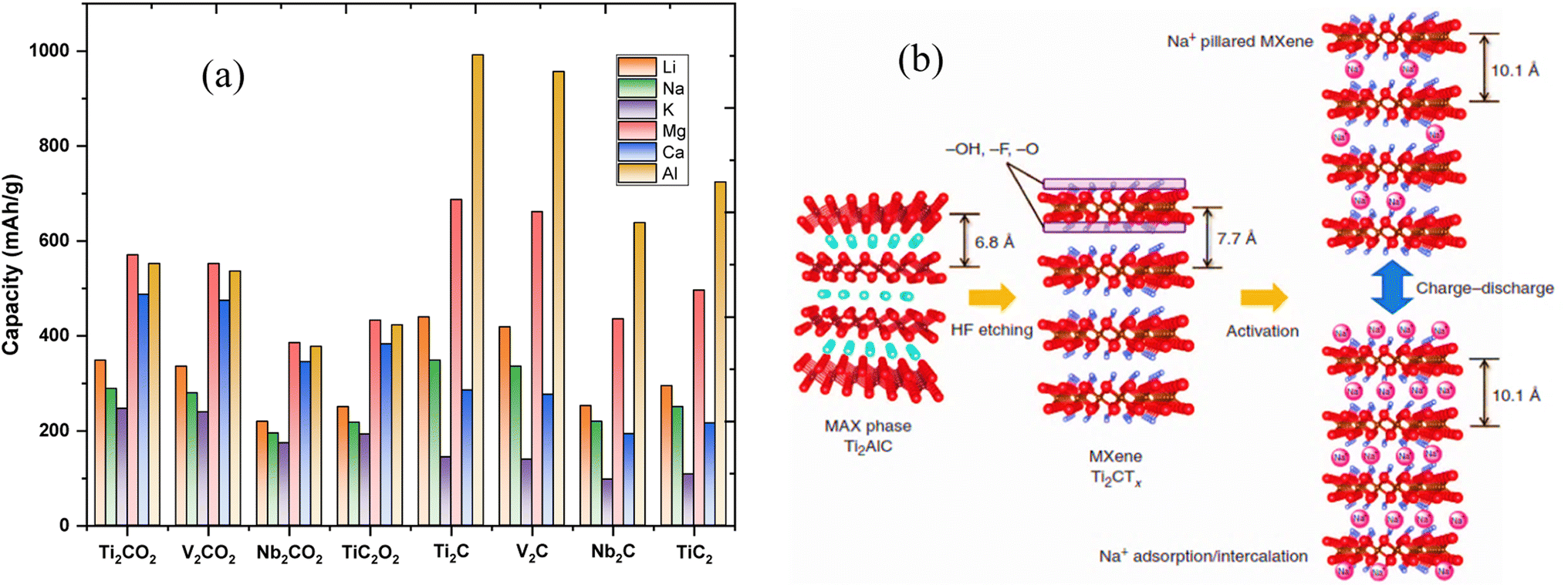 | ||
| Fig. 21 (a) A study of the storage capacities of various MXene materials. (b) Diagram of the electrochemical activation in the Ti2CTx reaction mechanism, where MXene Ti2CTx was created by HF treatment from the precursor Ti2AlC. The MXene Ti2CTx using expansion of Na+ intercalation and reversible Na+ (de)intercalation exhibits no alteration in interlayer distance. Reproduced from ref. 346 with permission from Springer Nature, copyright 2015. | ||
The films become more flexible and collect and store more ions on the surface of the pores thanks to the porous structure. A first-cycle capacity of 790 mA h g−1 is provided by a porous Ti3C2Tx alloy containing 10 wt% CNTs.347 A potential candidate for Li–S batteries is a 70 wt% Ti2C–S composite using Ti2C as the matrix. It has a storage capacity of 1090 mA h g−1 at C/2 and a very low decay rate of 0.05% per cycle.348 Comparably, a combination of layered Ti3C2 and 57.6 wt% sulfur has a capacity of 1291 mA h g−1 and can hold onto 970 mA h g−1 after 100 cycles.349 A simple liquid-phase immersion method is used to create a hybrid of 5 wt% Sn with Ti3C2.20,31 MXenes and absorber must therefore be properly paired in order to further improve energy storage.
MXenes are potential candidates for use in energy harvesting and conversion applications due to their mechanical stability and extremely negative triboelectric properties. Adaptable triboelectric nanogenerators (TENGs) can harvest power from human movement.350,351 At a matching load impedance of 4.5 M, a frequency of 4.5 Hz, and a force of 8 N, a fabric-based waterproof (FW-TENG) with MXene triboelectric produces 3.69 mW (maximum output peak power) and a power density of 9.24 W m−2.351 Ti3C2Tx is one of the finest materials for solar-powered water steam generation because of its extremely high light-to-heat conversion efficiency.352
High hydrogen evolution reaction (HER) in the materials results in a significant number of oxygen atom openings on the surface. Reducing fluorine concentrations and increasing oxygen concentrations, which serve as catalytic active sites for HER activity, can be used to successfully control MXene surface stoichiometry.353–355 The MXene surface must have greater oxygen and lower fluorine concentrations to be more catalytically effective toward HER.355 Compared to Ti3C2Tx or Ti2CTx, which have more fluorine, Mo-based Mo2CTx MXenes function better in HER tests.353,355 First-principles computations provide the hydrogen interaction with the MXene surface and in the vacancies. It demonstrates that the adsorption energy of hydrogen is sensitive to both surface coverage and vacancy occupancy and that thermoneutral values of hydrogen adsorption may be attained for certain structures with hydrogen in the vacancies. According to calculation, protons can move to vacancies at high cathodic potentials and remain there in a metastable state of hydrogen atoms, but at anodic potential the process is reversed. The first-principles results provide a rationale for the strongly enhanced HER activity that is observed experimentally on W1.33C and Mo4/3C MXenes.356 By creating gaps on M-sites, Mo2TiC2Cx exhibits enhanced catalytic activity for HER.357 The created catalyst exhibits performance overpotentials of 30 and 77 mV for 10 and 100 mA cm−2 (Fig. 22) and a mass activity that is about 40 times greater than that of a commercially available platinum-on-carbon catalyst. As a very effective oxygen electrode, a hybrid film (TCCN) comprising g-C3N4 and Ti3C2 nanosheets has been developed for overlaying. Through Ti–N interaction, Ti3C2 is joined to g-C3N4 to create a porous free-standing film with a hydrophilic surface and conductive framework that performs admirably in Zn-air batteries and OER catalysis.358 When MXene (Ti3C2Tx2) nanosheets are bonded to a vertically aligned metal host under ambient circumstances, they are able to produce NH3 at an extremely low potential with a high faradaic efficiency (5.78%). The increased activity of the basal plane of MXene, which is comparatively inert, is associated with the presence of more exposed edge sites. This work demonstrates that by adjusting active sites and delaying hydrogen evolution activity, NH3 electrosynthesis selectivity may be significantly increased in the N reduction reaction (NRR).359
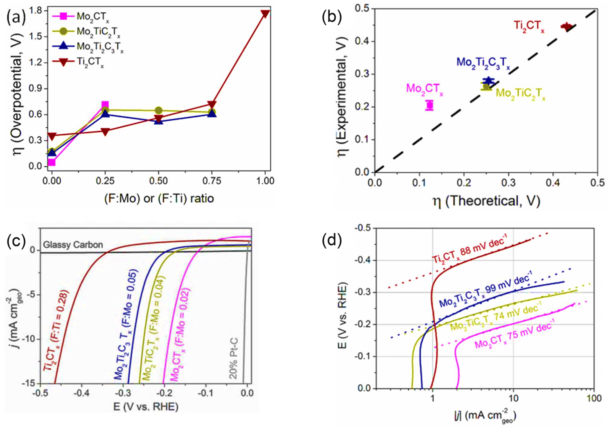 | ||
| Fig. 22 (a) DFT-calculated HER overpotential based on F basal plane coverage (F:Mo or F:Ti ratio). (b) Analysis of experimental and theoretical overpotentials. Ideal conditions that are consistent with theoretical numbers are shown by dashed lines. (c) Linear sweep voltammetry (LSV) used to measure HER activity, and (d) a Tafel diagram of MXenes in 0.5 M H2SO4. Reproduced from ref. 355 with permission from American Chemical Society, copyright 2018. | ||
Flexible solid-state supercapacitors have attracted a lot of interest for all types of electrochemical energy storage due to the fast development of modern wearable electronics.360–365 The fabrication of transparent electronic devices (TEDs) demands a fast charge–discharge rate, high capacitive nature, energy density, and long life under any distorting conditions. High-performance capacitors must have a high current flow and low energy wastage. Due to its high electrical conductivity of 15100 S cm−1 for a 214 nm-thick film, Ti3C2Tx is the most extensively researched material.366 Rolled sheets of Ti3C2Tx exhibit volumetric capacitances of up to 900 F cm−3 in 1 M H2SO4 electrolyte, and the capacitance remains constant even after 10000 cycles (Fig. 23).288 However, Ti3C2Tx paper, which is more pliable, offers 350 F cm−3.367 Comparably, 1315 F cm−3 is revealed by V2CTx particles in H2SO4 electrolyte, and they maintain 77% of their capacitance even after one million cycles at 100 A g−1.266 A hybrid electrode made of polyaniline and graphene encapsulated Ti2CTx exhibits an exceptional level of cycling stability and a volumetric capacitance of 1143 F cm−3 in 1 M H2SO4.368 Additionally, an Nb2CTx/CNT paper electrode, which has a polypropylene membrane, offers 325 F cm−3 capacitance at 5 mV s−1, but the performance degrades with rising scanning rate.369 Similar results are obtained with a Ti3C2Tx-CNT alloy, which exhibits 245 F cm−3 capacitance at 2 mV s−1.370 Due to the substantial interlayer spaces between the MXene sheets, a hybrid with a pyrrole to Ti3C2Tx ratio of 1:2 exhibits a volumetric capacitance of 1000 F cm−3 at 5 mV s−1 with 92% retention even after 25000 cycles.371 The electrochemical process can be managed and optimized using solid solutions of MXenes. With a rise in Nb content, Ti2−yNbyCTx and C2-yNbyCTx both exhibit a decrease in redox peak intensity and an improvement in cycling stability.372
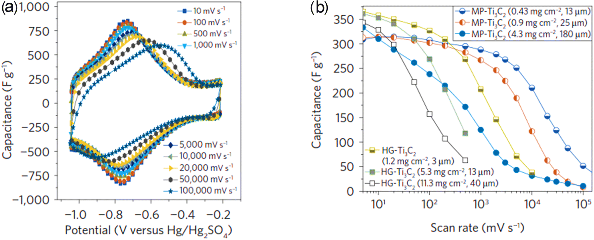 | ||
| Fig. 23 (a) Measurement of CV for a 90 nm thick Ti3C2Tx MXene at scan speeds ranging from 10 to 100000 mV s−1. (b) The gravimetric rate performance of MXene film preparation procedures and mass loading dependence. Reproduced from ref. 373 with permission from Springer Nature, copyright 2017. | ||
By using current collectors other than glassy carbon, such as graphite, an MXene electrode is able to push capacitance very close to its theoretical limit. Additionally, MXene macroporous electrode designs allow for exceptional capacitance withholding even at charge–discharge rates above 1 V s−1: 210 F g−1 at 10 V s−1 and 100 F g−1 at 40 V s−1, which are exceptional compared to the finest carbon supercapacitors known to man. Hydrogel electrodes outperformed state-of-the-art supercapacitor materials in terms of the volumetric performance of RuO2, demonstrating remarkable volumetric capacitance up to 1500 F cm−3 and areal capacitance up to 4 F cm−2.373
A quick charge–discharge rate, high capacitive nature, energy density, and a long life in any distorting situation are requirements for the fabrication of transparent electronic devices (TCDs). More than 90% transmittance and less than 100 sq−1 sheet resistance (Rs) of the electrode are required to accomplish these properties. Indium tin oxide has previously possessed these characteristics, but the development of this new industry is hampered by the inherent fragility of the material and its expensive fabrication costs.374,375 2D materials are presently thought to be emerging as a possible candidate to resolve every problem facing developing TCD industries. Flakes of Ti3C2Tx that are aligned in parallel exhibit remarkable success in producing low resistivity and high transmittance. MXene, which has a transmittance of over 90%, can provide Rs of 1032 sq−1, while graphene exhibits a value that is three times higher, as shown in Fig. 24.376–379 In another study, Ti3C2Tx film covering polyethylene terephthalate measured at 424 sq−1 Rs had 57% transmittance.380 Similarly, Ti3C2Tx alloy with silver nanowire that has undergone solution processing exhibits Rs of 13–15 sq−1 and 84–89% transmittance.381,382
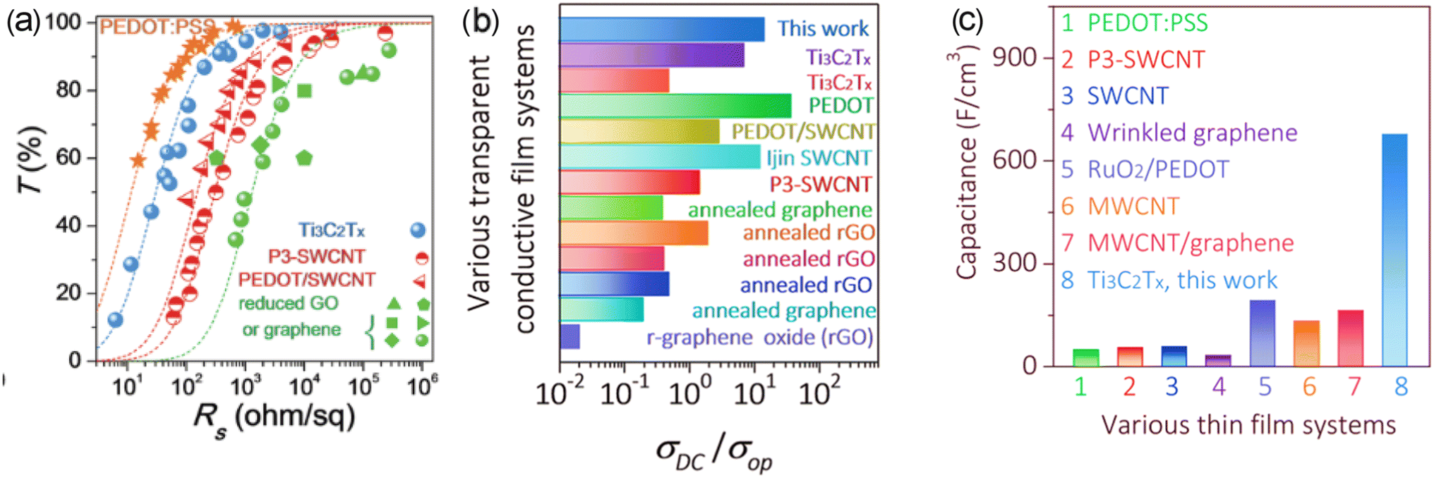 | ||
| Fig. 24 Optoelectronic properties of Ti3C2Tx films: (a) the transmittance (T) at 550 nm as a function of sheet resistance Rs and (b) comparison of Ti3C2Tx with other transparent thin films. (c) Comparison of σDC/σop in Ti3C2Tx films to various other transparent capacitive electrodes (TCEs). Reproduced from ref. 379 with permission from John Wiley and Sons, copyright 2017. | ||
Additionally, DC conductivity and bulk capacitance in relation to optical conductivity can be used to evaluate the competitiveness of a material for a TCD.379 MXene also has a higher DC to optical transmission ratio than other graphene materials, as shown in Fig. 24(b). MXene thin films also have the highest capacitance of any thin film.379 In comparison to other MXene composites, Ti3C2Tx and polycation layer-by-layer assembly provides 24 times more conductivity and 3 times better capacitance.383
Li-atom mobility computations show that M2C and M3C2 monolayered surfaces with notably low diffusion barriers—reportedly 0.01 eV for Ti2C, V2C, Sc2C, and Zr2C—have very high Li-atom mobility. It follows that multilayered transition-metal carbides might be employed as fast-charging electrode materials. More precisely, thorough experimental and theoretical studies are needed to examine the energy storage potential of Sc, Ti, V, and Zr based MXene materials. On the basis of this study, additional research on the electronic and optical characteristics of MXenes is also recommended, which could help to bridge the knowledge divide between theoretical predictions and experimental observations.
5. Concluding remarks
The current century is acknowledged by scientists to be the one of nanotechnology. One of the key elements in the advancement of nanotechnology is the creation of two-dimensional nanostructured materials (2D NSMs). Nanosheets of 2D NSMs and layered structured materials are widely studied because of their distinctive physicochemical characteristics. For 2D NSMs, efficient and approachable synthesis methods are more crucial. This review includes synthesis methods as well as the most recent advances in 2D NSM applications outside of graphene. Graphene is the perfect structure to comprehend the fundamental physiochemical characteristics of 2D NSMs and their applications. Different 2D NSMs other than graphene have recently become a very academically rigorous study area in 2D nanomaterials. 2D NSMs exhibit extremely intriguing electronic characteristics that are strikingly similar to or dissimilar from those of graphene. Due to the fact that their surface to volume ratios are different from those of their bulk counterpart, 2D NSMs actually exhibit distinctive physical and chemical properties. What is more exciting is that these properties can be excitingly tailored using strain, doping, and electric fields for many technological applications. These 2D layered materials are used in MEMS and NEMS electronic devices, energy storage devices, biosensors, supercapacitors, solar cells, and catalysts due to their versatile and excellent optical and electronic characteristics.There are difficulties in developing practical experimental methods for the massive manufacturing of monolayered and multilayered 2D NSMs. The most significant 2D materials beyond graphene are those with few layers and big surface areas. The optical, mechanical, chemical, and thermal properties of TMD and h-BN nanosheets, germanene, and silicene have not yet been fully revealed, despite intensive study of their electronic properties. Techniques for making MXenes have recently been developed, and a variety of their characteristics are currently the subject of extensive research. This review summarizes synthesis methods and discusses the difficulties and potential of MXenes; ideally, this will hasten the investigation of 2D NSMs other than graphene.
Even when silicon with a thin dielectric film is used, the transistor performance of TMD MX2 materials like MoS2 and WS2 is significantly enhanced. For the electronic sectors, the TMD semiconducting single layer has opened a door to ground-breaking and fascinating research. MoS2 has been the subject of intensive research, but little is known about the optical and electronic properties of metal chalcogenide nanosheets. Based on theoretical research, silicene and germanene exhibit almost identical graphene-like characteristics, but there is a severe lack of experimental data for these two materials. Additionally, the majority of research on germanene and silicene is conducted on metallic substrates, which are inappropriate for use in electronic devices. The fabrication of two materials on a non-metallic or insulating substrate presents a greater challenge. Beyond graphene, MXenes have been extensively explored using theoretical and experimental methods in 2D NSM. This review thoroughly explains the prospects and obstacles for MXenes, paving the way for the discovery of previously undiscovered properties. For the integration of MXenes on chips using conventional and widely available microfabrication device technology, a vapor-phase technique must be developed. To better comprehend the characteristics of MXenes, theoretical and experimental research must work together.
It is true that there is still much to learn about 2D compounds other than graphene. To address the challenges of nanotechnology, the peculiar properties of 2D NSMs can be unlocked and intriguing new breakthroughs made. New 2D NSMs with intriguing properties have been created after a lot of work and will be useful to the electronic sectors.
Conflicts of interest
The authors affirm that they have no known financial or interpersonal conflicts that might have looked to have an impact on the research presented in this paper.Abbreviation
| h-BN | Hexagonal boron nitride |
| BP | Black phosphorus |
| TMD | Transition metal dichalcogenides |
| MOFs | Metal–organic frameworks (MOFs) |
| LDHs | Layered double hydroxides |
| COFs | Covalent organic frameworks |
| Xenes | Monoelemental compounds metal oxides |
| TMHs | Transition metal halides |
| XRD | X-ray diffraction |
| SEM | Scanning electron microscope |
| TEM | Transmission electron microscope |
| STM | Scanning tunnelling microscopy |
| EELS | Electron energy loss spectra |
| AFM | Atomic force microscopy |
| PL | Photoluminescence |
| EDX | Energy dispersive X-ray analysis |
| DLS | Dynamic light scattering |
| GO | Graphene oxide |
| DFT | Density functional theory |
| UV | Ultraviolet |
| QLED | Quantum dot light-emitting diodes |
| HIL | Hole injection layer |
| LED | Light-emitting diodes |
| PV | Photovoltaics |
| GQDs | Graphene quantum dots |
| ConA | Concanavalin A |
| FRET | Fluorescence resonance energy transfer |
| ssDNA | Single-stranded deoxyribonucleic acid |
| PEG | Polyethylene glycol |
| SOC | Spin–orbit coupling |
| MBE | Molecular beam epitaxy |
| ARPES | Angle resolved photoemission spectroscopy |
| QSHE | Quantum spin Hall effect |
| FET | Field effect transistor |
| NM | Nonmagnetic |
| FM | Ferromagnetic |
| GGA | Generalized gradient approximation |
| EELS | Electron energy loss spectra |
| NMP | N-methylpyrrolidone |
| DMF | Dimethylformamide |
| DOX | Doxorubicin hydrochloride |
| BNNS | Boron nitride nanosheets |
| PMMA | Polymethyl methacrylate |
| BNONS | BN oxide nanosheets |
| DCE | 1,2-Dichloroethane |
| TFT | Thin film transistor |
| EDLC | Electrical double layer capacitance |
| SIBs | Sodium-ion batteries |
| LIBs | Lithium-ion batteries |
| DOS | Density of states |
| TIs | Topological insulator |
| TENGs | Flexible triboelectric nanogenerators |
| HER | Hydrogen evolution reaction |
| NRR | N reduction reactions |
| OER | Oxygen evolution reaction |
Acknowledgements
The Chittagong University of Engineering and Technology (CUET), Chattogram-4349, Bangladesh's Directorate of Research and Extension (DRE), for funding the research with the project number CUET/DRE/2020-2021/PHY/009, CUET/DRE/2021-22/PHY/011 and S. K. Mandal thanks the CSIR, Government of India, for giving the fellowship.References
- V. Singh, D. Joung, L. Zhai, S. Das, S. I. Khondaker and S. Seal, Prog. Mater. Sci., 2011, 56, 1178 CrossRef CAS.
- N. Yang, J. Zhai, D. Wang, Y. Chen and L. Jiang, ACS Nano, 2010, 4(2), 887 CrossRef CAS PubMed.
- S. Ghosh, B. K. Sarker, A. Chunder, L. Zhai and S. I. Khondaker, Appl. Phys. Lett., 2010, 96, 163109, DOI:10.1063/1.3415499.
- K. S. Novoselov, A. K. Geim, S. V Morozov, D. Jiang, Y. Zhang, S. V. Dubonos, I. V Grigorieva and A. A. Firsov, Science, 2004, 306, 666 CrossRef CAS PubMed.
- T. Kanazawa, T. Amemiya, A. Ishikawa, V. Upadhyaya, K. Tsuruta, T. Tanaka and Y. Miyamoto, Sci. Rep., 2016, 6, 22277, DOI:10.1038/srep22277.
- A. K. Geim and I. V. Grigorieva, Nature, 2013, 499, 419 CrossRef CAS PubMed.
- K. F. Mak, C. Lee, J. Hone, J. Shan and T. F. Heinz, Phys. Rev. Lett., 2010, 105, 136805, DOI:10.1103/PhysRevLett.105.136805.
- E. Canadell, A. LeBeuze, M. A. El Khalifa, R. Chevrel and M. H. Whangbo, J. Am. Chem. Soc., 1989, 111, 3778, DOI:10.1021/ja00193a002.
- M. A. Lukowski, A. S. Daniel, C. R. English, F. Meng, A. Forticaux, R. J. Hamers and S. Jin, Energy Environ. Sci., 2014, 7, 2608, 10.1039/c4ee01329h.
- A. N. Andriotis and M. Menon, Phys. Rev. B: Condens. Matter Mater. Phys., 2014, 90, 125304, DOI:10.1103/PhysRevB.90.125304.
- J. He, K. Hummer and C. Franchini, Phys. Rev. B: Condens. Matter Mater. Phys., 2014, 89, 075409, DOI:10.1103/PhysRevB.89.075409.
- Y. H. Huang, C. C. Peng, R. S. Chen, Y. S. Huang and C. H. Ho, Appl. Phys. Lett., 2014, 105, 093106, DOI:10.1063/1.4894857.
- D. B. Moore, M. Beekman, S. Disch, P. Zschack, I. Häusler, W. Neumann and D. C. Johnson, Chem. Mater., 2013, 25, 2404, DOI:10.1021/cm400090f.
- R. Ganatra and Q. Zhang, ACS Nano, 2014, 8, 4074 CrossRef CAS PubMed.
- B. Anasori, M. R. Lukatskaya and Y. Gogotsi, Nat. Rev. Mater., 2017, 2, 16098 CrossRef CAS.
- L. B. Gower, Chem. Rev., 2008, 108, 4551, DOI:10.1021/cr800443h.
- D. Gebauer and H. Cölfen, Nano Today, 2011, 6, 564 CrossRef CAS.
- J. Nai, H. Yin, T. You, L. Zheng, J. Zhang, P. Wang, Z. Jin, Y. Tian, J. Liu, Z. Tang and L. Guo, Adv. Energy Mater., 2015, 5, 1401880, DOI:10.1002/aenm.201401880.
- L. Deng, Z. Yang, L. Tan, L. Zeng, Y. Zhu and L. Guo, Adv. Mater., 2018, 30, 1802510, DOI:10.1002/adma.201802510.
- H. Zhao, X. Chen, G. Wang, Y. Qiu and L. Guo, 2d Mater., 2019, 6, 032002 CrossRef CAS.
- M. Alhabeb, K. Maleski, B. Anasori, P. Lelyukh, L. Clark, S. Sin and Y. Gogotsi, Chem. Mater., 2017, 29, 7633 CrossRef CAS.
- P. Ajayan, P. Kim and K. Banerjee, Phys. Today, 2016, 69, 38, DOI:10.1063/PT.3.3297.
- Y. Liu, N. O. Weiss, X. Duan, H. C. Cheng, Y. Huang and X. Duan, Nat. Rev. Mater., 2016, 1, 16042 CrossRef CAS.
- K. S. Novoselov, A. Mishchenko, A. Carvalho and A. H. Castro Neto, Science, 2016, 353, 6298 CrossRef PubMed.
- N. Briggs, S. Subramanian, Z. Lin, X. Li, X. Zhang, K. Zhang, K. Xiao, D. Geohegan, R. Wallace, L. Q. Chen, M. Terrones, A. Ebrahimi, S. Das, J. Redwing, C. Hinkle, K. Momeni, A. Van Duin, V. Crespi, S. Kar and J. A. Robinson, 2d Mater., 2019, 6, 022001 CrossRef CAS.
- P. Miró, M. Audiffred and T. Heine, Chem. Soc. Rev., 2014, 43, 6537 RSC.
- A. Bandyopadhyay and D. Jana, Rep. Prog. Phys., 2020, 83, 056501 CrossRef CAS PubMed.
- G. G. Naumis, S. Barraza-Lopez, M. Oliva-Leyva and H. Terrones, Rep. Prog. Phys., 2017, 80, 096501 CrossRef PubMed.
- Y. Zhang, A. Rubio and G. Le Lay, J. Phys. D Appl. Phys., 2017, 50, 053004 CrossRef.
- S. Balendhran, S. Walia, H. Nili, S. Sriram and M. Bhaskaran, Small, 2015, 11, 633, DOI:10.1002/smll.201570033.
- A. Gupta, T. Sakthivel and S. Seal, Prog. Mater. Sci., 2015, 73, 44 CrossRef CAS.
- V. K. Sangwan and M. C. Hersam, Annu. Rev. Phys. Chem., 2018, 69, 299, DOI:10.1146/annurev-physchem-050317-021353.
- A. H. Castro Neto, F. Guinea, N. M. R. Peres, K. S. Novoselov and A. K. Geim, Rev. Mod. Phys., 2009, 81, 109, DOI:10.1103/RevModPhys.81.109.
- D. R. Dreyer, S. Park, C. W. Bielawski and R. S. Ruoff, Chem. Soc. Rev., 2010, 39, 228 RSC.
- P. P. Brisebois and M. Siaj, J. Mater. Chem. C, 2020, 8, 1517 RSC.
- F. Farjadian, S. Abbaspour, M. A. A. Sadatlu, S. Mirkiani, A. Ghasemi, M. Hoseini-Ghahfarokhi, N. Mozaffari, M. Karimi and M. R. Hamblin, ChemistrySelect, 2020, 5, 10200 CrossRef CAS.
- R. Tarcan, O. Todor-Boer, I. Petrovai, C. Leordean, S. Astilean and I. Botiz, J. Mater. Chem. C, 2020, 8, 1198 RSC.
- R. K. Singh, R. Kumar and D. P. Singh, RSC Adv., 2016, 6, 64993 RSC.
- D. C. Marcano, D. V. Kosynkin, J. M. Berlin, A. Sinitskii, Z. Sun, A. Slesarev, L. B. Alemany, W. Lu and J. M. Tour, ACS Nano, 2010, 4, 4806, DOI:10.1021/nn1006368.
- D. C. Marcano, D. V. Kosynkin, J. M. Berlin, A. Sinitskii, Z. Sun, A. S. Slesarev, L. B. Alemany, W. Lu and J. M. Tour, ACS Nano, 2018, 12, 2078, DOI:10.1021/acsnano.8b00128.
- W. S. Hummers and R. E. Offeman, J. Am. Chem. Soc., 1958, 80, 1339, DOI:10.1021/ja01539a017.
- Z. Benzait, P. Chen and L. Trabzon, Nanoscale Adv., 2021, 3, 223, 10.1039/d0na00706d.
- R. Trusovas, G. Račiukaitis, G. Niaura, J. Barkauskas, G. Valušis and R. Pauliukaite, Adv. Opt. Mater., 2016, 4, 37, DOI:10.1002/adom.201500469.
- P. Ranjan, S. Agrawal, A. Sinha, T. R. Rao, J. Balakrishnan and A. D. Thakur, Sci. Rep., 2018, 8, 12007, DOI:10.1038/s41598-018-30613-4.
- S. Azizighannad and S. Mitra, Sci. Rep., 2018, 8, 10083, DOI:10.1038/s41598-018-28353-6.
- A. T. Smith, A. M. LaChance, S. Zeng, B. Liu and L. Sun, Nano Mater. Sci., 2019, 1, 31, DOI:10.1016/j.nanoms.2019.02.004.
- L. G. Guex, B. Sacchi, K. F. Peuvot, R. L. Andersson, A. M. Pourrahimi, V. Ström, S. Farris and R. T. Olsson, Nanoscale, 2017, 9, 9562, 10.1039/c7nr02943h.
- M. A. Khan, A. Kumar, J. Zhang and M. Kumar, J. Mater. Chem. C, 2021, 9, 3697 RSC.
- B. Chitara, L. S. Panchakarla, S. B. Krupanidhi and C. N. R. Rao, Adv. Mater., 2011, 23, 5419, DOI:10.1002/adma.201101414.
- P. E. Marchezi, F. L. de Araújo, R. Szostack, J. C. Germino, E. M. Therézio, A. Marletta and A. F. Nogueira, J. Mater. Chem. C, 2021, 9, 14648, 10.1039/d1tc01360b.
- Y. H. Lee, B. K. Kang, M. S. Kim, H. W. Choi, D. S. Choi, M. Kumar and D. H. Yoon, Phys. Status Solidi A, 2018, 215, 1700936, DOI:10.1002/pssa.201700936.
- S. K. Saha, S. Bhaumik, T. Maji, T. K. Mandal and A. J. Pal, RSC Adv., 2014, 4, 35493, 10.1039/c4ra03913k.
- P. S. Abid, S. S. Islam, P. Mishra and S. Ahmad, Sci. Rep., 2018, 8, 3537, DOI:10.1038/s41598-018-21686-2.
- B. Chitara, S. B. Krupanidhi and C. N. R. Rao, Appl. Phys. Lett., 2011, 99, 113114, DOI:10.1063/1.3640222.
- A. Mondal, A. Prabhakaran, S. Gupta and V. R. Subramanian, ACS Omega, 2021, 6, 8734 CrossRef CAS PubMed.
- P. Zheng and N. Wu, Chem.–Asian J., 2017, 12, 2343 CrossRef CAS PubMed.
- H. Zhang, H. Zhang, A. Aldalbahi, X. Zuo, C. Fan and X. Mi, Biosens. Bioelectron., 2017, 89, 96 CrossRef CAS PubMed.
- L. Wang, K.-Y. Pu, J. Li, X. Qi, H. Li, H. Zhang, C. Fan and B. Liu, Adv. Mater., 2011, 23, 4386 CrossRef CAS PubMed.
- J. H. Jung, D. S. Cheon, F. Liu, K. B. Lee and T. S. Seo, Angew. Chem., Int. Ed., 2010, 49, 5708 CrossRef CAS PubMed.
- E. Campbell, M. T. Hasan, C. Pho, K. Callaghan, G. R. Akkaraju and A. V. Naumov, Sci. Rep., 2019, 9, 416, DOI:10.1038/s41598-018-36617-4.
- L. Cunci, V. González-Colón, B. Lee Vargas-Pérez, J. Ortiz-Santiago, M. Pagán, P. Carrion, J. Cruz, A. Molina-Ontoria, N. Martinez, W. Silva, L. Echegoyen and C. R. Cabrera, ACS Appl. Nano Mater., 2021, 4, 211, DOI:10.1021/acsanm.0c02526.
- S. Chowdhury and D. Jana, Rep. Prog. Phys., 2016, 79, 126501, DOI:10.1088/0034-4885/79/12/126501.
- J. Zhao, H. Liu, Z. Yu, R. Quhe, S. Zhou, Y. Wang, C. C. Liu, H. Zhong, N. Han, J. Lu, Y. Yao and K. Wu, Prog. Mater. Sci., 2016, 83, 24 CrossRef CAS.
- P. Ramasami, Computational Sciences, Berlin, Boston, De Gruyter, 2017, DOI:10.1515/9783110467215.
- A. Fleurence, R. Friedlein, T. Ozaki, H. Kawai, Y. Wang and Y. Yamada-Takamura, Phys. Rev. Lett., 2012, 108, 245501, DOI:10.1103/PhysRevLett.108.245501.
- L. Meng, Y. Wang, L. Zhang, S. Du, R. Wu, L. Li, Y. Zhang, G. Li, H. Zhou, W. A. Hofer and H. J. Gao, Nano Lett., 2013, 13, 685, DOI:10.1021/nl304347w.
- P. Vogt, P. De Padova, C. Quaresima, J. Avila, E. Frantzeskakis, M. C. Asensio, A. Resta, B. Ealet and G. Le Lay, Phys. Rev. Lett., 2012, 108, 155501, DOI:10.1103/PhysRevLett.108.155501.
- E. Cinquanta, E. Scalise, D. Chiappe, C. Grazianetti, B. Van Den Broek, M. Houssa, M. Fanciulli and A. Molle, J. Phys. Chem. C, 2013, 117, 16719, DOI:10.1021/jp405642g.
- C. L. Lin, R. Arafune, K. Kawahara, N. Tsukahara, E. Minamitani, Y. Kim, N. Takagi and M. Kawai, Appl. Phys. Express, 2012, 5, 045802, DOI:10.1143/APEX.5.045802.
- B. Feng, Z. Ding, S. Meng, Y. Yao, X. He, P. Cheng, L. Chen and K. Wu, Nano Lett., 2012, 12, 3507, DOI:10.1021/nl301047g.
- A. Bhattacharya, S. Bhattacharya and G. P. Das, Appl. Phys. Lett., 2013, 103, 123113, DOI:10.1063/1.4821993.
- A. Acun, L. Zhang, P. Bampoulis, M. Farmanbar, A. Van Houselt, A. N. Rudenko, M. Lingenfelder, G. Brocks, B. Poelsema, M. I. Katsnelson and H. J. W. Zandvliet, J. Phys.: Condens.Matter, 2015, 27, 443002 CrossRef CAS PubMed.
- M. E. Dávila, L. Xian, S. Cahangirov, A. Rubio and G. Le Lay, New J. Phys., 2014, 16, 095002, DOI:10.1088/1367-2630/16/9/095002.
- L. Li, S. Z. Lu, J. Pan, Z. Qin, Y. Q. Wang, Y. Wang, G. Y. Cao, S. Du and H. J. Gao, Adv. Mater., 2014, 26, 4820, DOI:10.1002/adma.201400909.
- C. C. Liu, H. Jiang and Y. Yao, Phys. Rev. B: Condens. Matter Mater. Phys., 2011, 84, 195430, DOI:10.1103/PhysRevB.84.195430.
- A. Nijamudheen, R. Bhattacharjee, S. Choudhury and A. Datta, J. Phys. Chem. C, 2015, 119, 3802, DOI:10.1021/jp511488m.
- H. Behera and G. Mukhopadhyay, AIP Conf. Proc., 2011, 1349, 823 CrossRef CAS.
- Q. Pang, L. Li, C. L. Zhang, X. M. Wei and Y. L. Song, Mater. Chem. Phys., 2015, 160, 96, DOI:10.1016/j.matchemphys.2015.04.011.
- N. Dhar, A. Bandyopadhyay and D. Jana, Curr. Appl. Phys., 2017, 17, 573, DOI:10.1016/j.cap.2017.02.003.
- F. López-Urías, M. Terrones and H. Terrones, Carbon, 2015, 84, 317, DOI:10.1016/j.carbon.2014.11.053.
- N. Dhar and D. Jana, Curr. Appl. Phys., 2017, 17, 1589, DOI:10.1016/j.cap.2017.08.022.
- W. Xia, W. Hu, Z. Li and J. Yang, Phys. Chem. Chem. Phys., 2014, 16, 22495, 10.1039/c4cp03292f.
- H. H. Gürel, V. O. Özçelik and S. Ciraci, J. Phys.: Condens. Matter, 2013, 25, 305007, DOI:10.1088/0953-8984/25/30/305007.
- P. Jamdagni, A. Kumar, M. Sharma, A. Thakur and P. K. Ahluwalia, Phys. E, 2017, 85, 65, DOI:10.1016/j.physe.2016.08.015.
- Y. P. Wang, W. X. Ji, C. W. Zhang, S. S. Li, F. Li, P. Li, M. J. Ren, X. L. Chen, M. Yuan and P. J. Wang, Mater. Chem. Phys., 2016, 173, 379, DOI:10.1016/j.matchemphys.2016.02.026.
- N. Dhar and D. Jana, J. Phys. Chem. Solids, 2018, 115, 332, DOI:10.1016/j.jpcs.2017.12.055.
- F. bao Zheng and C. wen Zhang, Nanoscale Res. Lett., 2012, 7, 422, DOI:10.1186/1556-276X-7-422.
- J. Sivek, H. Sahin, B. Partoens and F. M. Peeters, Phys. Rev. B: Condens. Matter Mater. Phys., 2013, 87, 085444, DOI:10.1103/PhysRevB.87.085444.
- R. Das, S. Chowdhury, A. Majumdar and D. Jana, RSC Adv., 2015, 5, 41, 10.1039/c4ra07976k.
- S. Chowdhury, P. Nath and D. Jana, J. Phys. Chem. Solids, 2015, 83, 32, DOI:10.1016/j.jpcs.2015.03.017.
- M. Houssa, A. Dimoulas and A. Molle, J. Phys.: Condens. Matter, 2015, 27, 253002, DOI:10.1088/0953-8984/27/25/253002.
- E. Scalise, M. Houssa, E. Cinquanta, C. Grazianetti, B. Van Den Broek, G. Pourtois, A. Stesmans, M. Fanciulli and A. Molle, 2d Mater, 2014, 1, 011010, DOI:10.1088/2053-1583/1/1/011010.
- R. M. Ribeiro, V. M. Pereira, N. M. R. Peres, P. R. Briddon and A. H. Castro Neto, New J. Phys., 2009, 11, 115002, DOI:10.1088/1367-2630/11/11/115002.
- B. Mohan, A. Kumar and P. K. Ahluwalia, Phys. E, 2014, 61, 40, DOI:10.1016/j.physe.2014.03.013.
- G. Cheng, P. F. Liu and Z. T. Li, Chin. Phys. B, 2013, 22, 046201, DOI:10.1088/1674-1056/22/4/046201.
- Y. Wang and Y. Ding, Solid State Commun., 2013, 155, 6, DOI:10.1016/j.ssc.2012.10.044.
- G. Liu, M. S. Wu, C. Y. Ouyang and B. Xu, Europhys. Lett., 2012, 99, 17010, DOI:10.1209/0295-5075/99/17010.
- T. Hussain, T. Kaewmaraya, S. Chakraborty, H. Vovusha, V. Amornkitbamrung and R. Ahuja, ACS Sens., 2018, 3, 867, DOI:10.1021/acssensors.8b00167.
- S. Ghosal, A. Bandyopadhyay, S. Chowdhury and D. Jana, Rep. Prog. Phys., 2023, 86, 096502 CrossRef PubMed.
- J. Ding, H. Zhao, Q. Wang, W. Peng and H. Yu, Nanotechnology, 2017, 28, 475602, DOI:10.1088/1361-6528/aa8e3d.
- J. Ding, H. Zhao, Y. Zheng, Q. Wang, H. Chen, H. Dou and H. Yu, Nanotechnology, 2018, 29, 095603, DOI:10.1088/1361-6528/aaa05f.
- F. Xiao, S. Naficy, G. Casillas, M. H. Khan, T. Katkus, L. Jiang, H. Liu, H. Li and Z. Huang, Adv. Mater., 2015, 27, 7196, DOI:10.1002/adma.201502803.
- J. C. Zheng, L. Zhang, A. V. Kretinin, S. V. Morozov, Y. B. Wang, T. Wang, X. Li, F. Ren, J. Zhang, C. Y. Lu, J. C. Chen, M. Lu, H. Q. Wang, A. K. Geim and K. S. Novoselov, 2d Mater, 2016, 3, 011004, DOI:10.1088/2053-1583/3/1/011004.
- W. Lei, V. N. Mochalin, D. Liu, S. Qin, Y. Gogotsi and Y. Chen, Nat. Commun., 2015, 6, 8849, DOI:10.1038/ncomms9849.
- L. Niu, J. N. Coleman, H. Zhang, H. Shin, M. Chhowalla and Z. Zheng, Small, 2015, 12, 272, DOI:10.1002/smll.201502207.
- D. Paciĺ, J. C. Meyer, Ç. Girit and A. Zettl, Appl. Phys. Lett., 2008, 92, 133107, DOI:10.1063/1.2903702.
- J. C. Meyer, A. Chuvilin, G. Algara-Siller, J. Biskupek and U. Kaiser, Nano Lett., 2009, 9, 2683, DOI:10.1021/nl9011497.
- N. Alem, R. Erni, C. Kisielowski, M. D. Rossell, W. Gannett and A. Zettl, Phys. Rev. B: Condens. Matter Mater. Phys., 2009, 80, 155425, DOI:10.1103/PhysRevB.80.155425.
- A. Nagashima, N. Tejima, Y. Gamou, T. Kawai and C. Oshima, Phys. Rev. Lett., 1995, 75, 3918, DOI:10.1103/PhysRevLett.75.3918.
- C. Tang, Y. Bando, T. Sato and K. Kurashima, Chem. Commun., 2002, 1290, 10.1039/b202177c.
- J. Wang, C. H. Lee and Y. K. Yap, Nanoscale, 2010, 2, 2028 RSC.
- Y. Chen, L. T. Chadderton, J. F. Gerald and J. S. Williams, Appl. Phys. Lett., 1999, 74, 2960, DOI:10.1063/1.123979.
- J. K. Myung, S. Chatterjee, M. K. Seung, E. A. Stach, M. G. Bradley, M. J. Pender, L. G. Sneddon and B. Maruyama, Nano Lett., 2008, 8, 3298, DOI:10.1021/nl8016835.
- K. F. Huo, Z. Hu, J. J. Fu, H. Xu, X. Z. Wang, Y. Chen and Y. N. Lü, J. Phys. Chem. B, 2003, 107, 11316, DOI:10.1021/jp035375w.
- J. J. Fu, Y. N. Lu, H. Xu, K. F. Huo, X. Z. Wang, L. Li, Z. Hu and Y. Chen, Nanotechnology, 2004, 15, 727, DOI:10.1088/0957-4484/15/7/003.
- P. Gleize, M. C. Schouler, P. Gadelle and M. Caillet, J. Mater. Sci., 1994, 29, 1575, DOI:10.1007/BF00368928.
- D. P. Yu, X. S. Sun, C. S. Lee, I. Bello, S. T. Lee, H. D. Gu, K. M. Leung, G. W. Zhou, Z. F. Dong and Z. Zhang, Appl. Phys. Lett., 1998, 72, 1966, DOI:10.1063/1.121236.
- R. Arenal, O. Stephan, J. Lou Cochon and A. Loiseau, J. Am. Chem. Soc., 2007, 129, 16183, DOI:10.1021/ja076135n.
- M. W. Smith, K. C. Jordan, C. Park, J. W. Kim, P. T. Lillehei, R. Crooks and J. S. Harrison, Nanotechnology, 2009, 20, 505604, DOI:10.1088/0957-4484/20/50/505604.
- Y. Shimizu, Y. Moriyoshi, H. Tanaka and S. Komatsu, Appl. Phys. Lett., 1999, 75, 929, DOI:10.1063/1.124557.
- K. S. Kim, C. T. Kingston, A. Hrdina, M. B. Jakubinek, J. Guan, M. Plunkett and B. Simard, ACS Nano, 2014, 8, 6211, DOI:10.1021/nn501661p.
- A. Fathalizadeh, T. Pham, W. Mickelson and A. Zettl, Nano Lett., 2014, 14, 4881, DOI:10.1021/nl5022915.
- E. K. Sichel, R. E. Miller, M. S. Abrahams and C. J. Buiocchi, Phys. Rev. B: Condens. Matter Mater. Phys., 1976, 13, 4607, DOI:10.1103/PhysRevB.13.4607.
- A. Zunger, A. Katzir and A. Halperin, Phys. Rev. B: Condens. Matter Mater. Phys., 1976, 13, 5560, DOI:10.1103/PhysRevB.13.5560.
- S. Roy, X. Zhang, A. B. Puthirath, A. Meiyazhagan, S. Bhattacharyya, M. M. Rahman, G. Babu, S. Susarla, S. K. Saju, M. K. Tran, L. M. Sassi, M. A. S. R. Saadi, J. Lai, O. Sahin, S. M. Sajadi, B. Dharmarajan, D. Salpekar, N. Chakingal, A. Baburaj, X. Shuai, A. Adumbumkulath, K. A. Miller, J. M. Gayle, A. Ajnsztajn, T. Prasankumar, V. V. J. Harikrishnan, V. Ojha, H. Kannan, A. Z. Khater, Z. Zhu, S. A. Iyengar, P. A. da S. Autreto, E. F. Oliveira, G. Gao, A. G. Birdwell, M. R. Neupane, T. G. Ivanov, J. Taha-Tijerina, R. M. Yadav, S. Arepalli, R. Vajtai and P. M. Ajayan, Adv. Mater., 2021, 33, 2101589 CrossRef CAS PubMed.
- X. Blase, A. Rubio, S. G. Louie and M. L. Cohen, Phys. Rev. B: Condens. Matter Mater. Phys., 1995, 51, 6868, DOI:10.1103/PhysRevB.51.6868.
- H. Wang, X. Zhang, H. Liu, Z. Yin, J. Meng, J. Xia, X. M. Meng, J. Wu and J. You, Adv. Mater., 2015, 27, 8109, DOI:10.1002/adma.201504042.
- Q. Weng, D. G. Kvashnin, X. Wang, O. Cretu, Y. Yang, M. Zhou, C. Zhang, D. M. Tang, P. B. Sorokin, Y. Bando and D. Golberg, Adv. Mater., 2017, 29, 1700695, DOI:10.1002/adma.201700695.
- M. H. Tahersima and V. J. Sorger, Nanotechnology, 2015, 26, 344005, DOI:10.1088/0957-4484/26/34/344005.
- L. Lindsay and D. A. Broido, Phys. Rev. B: Condens. Matter Mater. Phys., 2012, 85, 035436, DOI:10.1103/PhysRevB.85.035436.
- P. Jiang, X. Qian, R. Yang and L. Lindsay, Phys. Rev. Mater., 2018, 2, 064005, DOI:10.1103/PhysRevMaterials.2.064005.
- A. Simpson and A. D. Stuckes, J. Phys. C: Solid State Phys., 1971, 4, 1710, DOI:10.1088/0022-3719/4/13/021.
- C. Yuan, J. Li, L. Lindsay, D. Cherns, J. W. Pomeroy, S. Liu, J. H. Edgar and M. Kuball, Commun. Phys., 2019, 2, 43, DOI:10.1038/s42005-019-0145-5.
- Q. Peng, W. Ji and S. De, Comput. Mater. Sci., 2012, 56, 11, DOI:10.1016/j.commatsci.2011.12.029.
- L. Song, L. Ci, H. Lu, P. B. Sorokin, C. Jin, J. Ni, A. G. Kvashnin, D. G. Kvashnin, J. Lou, B. I. Yakobson and P. M. Ajayan, Nano Lett., 2010, 10, 3209, DOI:10.1021/nl1022139.
- C. Li, Y. Bando, C. Zhi, Y. Huang and D. Golberg, Nanotechnology, 2009, 20, 385707, DOI:10.1088/0957-4484/20/38/385707.
- E. Hernández, C. Goze, P. Bernier and A. Rubio, Phys. Rev. Lett., 1998, 80, 4502 CrossRef.
- S. J. Cartamil-Bueno, M. Cavalieri, R. Wang, S. Houri, S. Hofmann and H. S. J. van der Zant, npj 2D Mater. Appl., 2017, 1, 16, DOI:10.1038/s41699-017-0020-8.
- S. M. Kim, A. Hsu, M. H. Park, S. H. Chae, S. J. Yun, J. S. Lee, D. H. Cho, W. Fang, C. Lee, T. Palacios, M. Dresselhaus, K. K. Kim, Y. H. Lee and J. Kong, Nat. Commun., 2015, 6, 8662, DOI:10.1038/ncomms9662.
- R. Y. Tay, H. J. Park, G. H. Ryu, D. Tan, S. H. Tsang, H. Li, W. Liu, E. H. T. Teo, Z. Lee, Y. Lifshitz and R. S. Ruoff, Nanoscale, 2016, 8, 2434, 10.1039/c5nr08036c.
- C. W. Chang, W.-Q. Han and A. Zettl, J. Vac. Sci. Technol. B, 2005, 23, 1883, DOI:10.1116/1.2008266.
- Y. Lin and J. W. Connell, Nanoscale, 2012, 4, 6908 RSC.
- H. Åžahin, M. Topsakal and S. Ciraci, Phys. Rev. B: Condens. Matter Mater. Phys., 2011, 83, 115432, DOI:10.1103/PhysRevB.83.115432.
- C. Zhi, Y. Bando, C. Tang, H. Kuwahara and D. Golberg, Adv. Mater., 2009, 21, 2889, DOI:10.1002/adma.200900323.
- C. S. Boland, S. Barwich, U. Khan and J. N. Coleman, Carbon, 2016, 99, 280, DOI:10.1016/j.carbon.2015.12.023.
- J. Liu, W. Li, Y. Guo, H. Zhang and Z. Zhang, Composites, Part A, 2019, 120, 140, DOI:10.1016/j.compositesa.2019.02.026.
- T. Özdemir and S. N. Yılmaz, Radiat. Phys. Chem., 2018, 152, 93, DOI:10.1016/j.radphyschem.2018.08.008.
- Q. Weng, B. Wang, X. Wang, N. Hanagata, X. Li, D. Liu, X. Wang, X. Jiang, Y. Bando and D. Golberg, ACS Nano, 2014, 8, 6123, DOI:10.1021/nn5014808.
- A. Sajid, M. J. Ford and J. R. Reimers, Rep. Prog. Phys., 2020, 83, 044501 CrossRef CAS PubMed.
- J. D. Caldwell, I. Aharonovich, G. Cassabois, J. H. Edgar, B. Gil and D. N. Basov, Nat. Rev. Mater., 2019, 4, 552–567 CrossRef CAS.
- Z. Jacob, Nat. Mater., 2014, 13, 044501 CrossRef PubMed.
- S. Dai, Z. Fei, Q. Ma, A. S. Rodin, M. Wagner, A. S. McLeod, M. K. Liu, W. Gannett, W. Regan, K. Watanabe, T. Taniguchi, M. Thiemens, G. Dominguez, A. H. Castro Neto, A. Zettl, F. Keilmann, P. Jarillo-Herrero, M. M. Fogler and D. N. Basov, Science, 2014, 343, 1125, DOI:10.1126/science.1246833.
- R. Bourrellier, S. Meuret, A. Tararan, O. Stéphan, M. Kociak, L. H. G. Tizei and A. Zobelli, Nano Lett., 2016, 16, 4317, DOI:10.1021/acs.nanolett.6b01368.
- T. T. Tran, K. Bray, M. J. Ford, M. Toth and I. Aharonovich, Nat. Nanotechnol., 2016, 11, 37, DOI:10.1038/nnano.2015.242.
- G. Grosso, H. Moon, B. Lienhard, S. Ali, D. K. Efetov, M. M. Furchi, P. Jarillo-Herrero, M. J. Ford, I. Aharonovich and D. Englund, Nat. Commun., 2017, 8, 705, DOI:10.1038/s41467-017-00810-2.
- N. Mendelson, M. Doherty, M. Toth, I. Aharonovich and T. T. Tran, Adv. Mater., 2020, 32, 1908316, DOI:10.1002/adma.201908316.
- H. Zhang, C. J. Tong, Y. Zhang, Y. N. Zhang and L. M. Liu, J. Mater. Chem. A, 2015, 3, 9632, 10.1039/c5ta01052g.
- S. H. Lim, J. Luo, W. Ji and J. Lin, Catal. Today, 2007, 120, 346, DOI:10.1016/j.cattod.2006.09.016.
- A. Lale, S. Bernard and U. B. Demirci, Chempluschem, 2018, 83, 893 CrossRef CAS PubMed.
- Q. Weng, X. Wang, C. Zhi, Y. Bando and D. Golberg, ACS Nano, 2013, 7, 1558, DOI:10.1021/nn305320v.
- S. Yu, X. Wang, H. Pang, R. Zhang, W. Song, D. Fu, T. Hayat and X. Wang, Chem. Eng. J., 2018, 333, 343 CrossRef CAS.
- W. Lei, D. Portehault, D. Liu, S. Qin and Y. Chen, Nat. Commun., 2013, 4, 1777, DOI:10.1038/ncomms2818.
- W. Hao, C. Marichy, C. Journet and A. Brioude, ChemNanoMat, 2017, 3, 656, DOI:10.1002/cnma.201700148.
- M. Weber, I. Iatsunskyi, E. Coy, P. Miele, D. Cornu and M. Bechelany, Adv. Mater. Interfaces, 2018, 5, 1800056, DOI:10.1002/admi.201800056.
- M. Emanet, Ö. Şen and M. Çulha, Nanomedicine, 2017, 12, 797, DOI:10.2217/nnm-2016-0322.
- E. Duverger, S. Balme, M. Bechelany, P. Miele and F. Picaud, Appl. Surf. Sci., 2019, 475, 666, DOI:10.1016/j.apsusc.2018.12.273.
- M. Li, G. Huang, X. Chen, J. Yin, P. Zhang, Y. Yao, J. Shen, Y. Wu and J. Huang, Perspectives on environmental applications of hexagonal boron nitride nanomaterials, Nano Today, 2022, 44, 101486, DOI:10.1016/j.nantod.2022.101486.
- A. H. Castro Neto and F. Guinea, Phys. Rev. Lett., 2009, 103, 026804, DOI:10.1103/PhysRevLett.103.026804.
- R. G. Dickinson and L. Pauling, J. Am. Chem. Soc., 1923, 45, 1466 CrossRef CAS.
- R. F. Frindt and A. D. Yoffe, Proc. R. Soc. London, Ser. A, 1963, 273, 69, DOI:10.1098/rspa.1963.0075.
- P. Joensen, R. F. Frindt and S. R. Morrison, Mater. Res. Bull., 1986, 21, 457, DOI:10.1016/0025-5408(86)90011-5.
- H. Li, G. Lu, Y. Wang, Z. Yin, C. Cong, Q. He, L. Wang, F. Ding, T. Yu and H. Zhang, Small, 2012, 9, 1974, DOI:10.1002/smll.201202919.
- J. N. Coleman, M. Lotya, A. O'Neill, S. D. Bergin, P. J. King, U. Khan, K. Young, A. Gaucher, S. De, R. J. Smith, I. V. Shvets, S. K. Arora, G. Stanton, H. Y. Kim, K. Lee, G. T. Kim, G. S. Duesberg, T. Hallam, J. J. Boland, J. J. Wang, J. F. Donegan, J. C. Grunlan, G. Moriarty, A. Shmeliov, R. J. Nicholls, J. M. Perkins, E. M. Grieveson, K. Theuwissen, D. W. McComb, P. D. Nellist and V. Nicolosi, Science, 2011, 331, 568 CrossRef CAS PubMed.
- G. Eda, H. Yamaguchi, D. Voiry, T. Fujita, M. Chen and M. Chhowalla, Nano Lett., 2011, 11, 5111 CrossRef CAS PubMed.
- K. K. Kim, A. Hsu, X. Jia, S. M. Kim, Y. Shi, M. Hofmann, D. Nezich, J. F. Rodriguez-Nieva, M. Dresselhaus, T. Palacios and J. Kong, Nano Lett., 2012, 12, 161, DOI:10.1021/nl203249a.
- H. S. S. Ramakrishna Matte, A. Gomathi, A. K. Manna, D. J. Late, R. Datta, S. K. Pati and C. N. R. Rao, Angew. Chem., Int. Ed., 2010, 49, 4059, DOI:10.1002/anie.201000009.
- K. S. Novoselov, A. K. Geim, S. V. Morozov, D. Jiang, M. I. Katsnelson, I. V. Grigorieva, S. V. Dubonos and A. A. Firsov, Nature, 2005, 438, 197, DOI:10.1038/nature04233.
- H. Li, J. Wu, Z. Yin and H. Zhang, Acc. Chem. Res., 2014, 47, 1067, DOI:10.1021/ar4002312.
- H. Li, J. Wu, X. Huang, G. Lu, J. Yang, X. Lu, Q. Xiong and H. Zhang, ACS Nano, 2013, 7, 10344, DOI:10.1021/nn4047474.
- A. E. Del Rio-Castillo, C. Merino, E. Díez-Barra and E. Vázquez, Nano Res., 2014, 7, 963, DOI:10.1007/s12274-014-0457-4.
- J. Chen, M. Duan and G. Chen, J. Mater. Chem., 2012, 22, 19625, 10.1039/c2jm33740a.
- K. S. Novoselov, D. Jiang, F. Schedin, T. J. Booth, V. V. Khotkevich, S. V. Morozov and A. K. Geim, Proc. Natl. Acad. Sci. U. S. A., 2005, 102, 10451, DOI:10.1073/pnas.0502848102.
- F. Torrisi, T. Hasan, W. Wu, Z. Sun, A. Lombardo, T. S. Kulmala, G. W. Hsieh, S. Jung, F. Bonaccorso, P. J. Paul, D. Chu and A. C. Ferrari, ACS Nano, 2012, 6, 2992, DOI:10.1021/nn2044609.
- X. Zeng, H. Hirwa, S. Metel, V. Nicolosi and V. Wagner, Solid-State Electron., 2018, 141, 58, DOI:10.1016/j.sse.2017.12.005.
- P. Blake, P. D. Brimicombe, R. R. Nair, T. J. Booth, D. Jiang, F. Schedin, L. A. Ponomarenko, S. V. Morozov, H. F. Gleeson, E. W. Hill, A. K. Geim and K. S. Novoselov, Nano Lett., 2008, 8, 1704, DOI:10.1021/nl080649i.
- J. Xiao, D. Choi, L. Cosimbescu, P. Koech, J. Liu and J. P. Lemmon, Chem. Mater., 2010, 22, 4522, DOI:10.1021/cm101254j.
- A. Jawaid, D. Nepal, K. Park, M. Jespersen, A. Qualley, P. Mirau, L. F. Drummy and R. A. Vaia, Chem. Mater., 2016, 28, 337, DOI:10.1021/acs.chemmater.5b04224.
- J. N. Coleman, M. Lotya, A. O'Neill, S. D. Bergin, P. J. King, U. Khan, K. Young, A. Gaucher, S. De, R. J. Smith, I. V. Shvets, S. K. Arora, G. Stanton, H. Y. Kim, K. Lee, G. T. Kim, G. S. Duesberg, T. Hallam, J. J. Boland, J. J. Wang, J. F. Donegan, J. C. Grunlan, G. Moriarty, A. Shmeliov, R. J. Nicholls, J. M. Perkins, E. M. Grieveson, K. Theuwissen, D. W. McComb, P. D. Nellist and V. Nicolosi, Science, 2011, 331, 568, DOI:10.1126/science.1194975.
- M. B. Dines, Mater. Res. Bull., 1975, 10, 287, DOI:10.1016/0025-5408(75)90115-4.
- Y. Yong, L. Zhou, Z. Gu, L. Yan, G. Tian, X. Zheng, X. Liu, X. Zhang, J. Shi, W. Cong, W. Yin and Y. Zhao, Nanoscale, 2014, 6, 10394, 10.1039/c4nr02453b.
- K. Kang, S. Chen and E. H. Yang, Synthesis, Modelling and Characterization of 2D Materials and their Heterostructures, 2020, p. 247 Search PubMed.
- M. B. Dines, Mater. Res. Bull., 1975, 10, 287 CrossRef CAS.
- Z. Zeng, Z. Yin, X. Huang, H. Li, Q. He, G. Lu, F. Boey and H. Zhang, Angew. Chem., Int. Ed., 2011, 50, 11093, DOI:10.1002/anie.201106004.
- G. Eda, H. Yamaguchi, D. Voiry, T. Fujita, M. Chen and M. Chhowalla, Nano Lett., 2011, 11, 5111 CrossRef CAS PubMed.
- R. A. Gordon, D. Yang, E. D. Crozier, D. T. Jiang and R. F. Frindt, Phys. Rev. B: Condens. Matter Mater. Phys., 2002, 65, 125407 CrossRef.
- G. Eda, H. Yamaguchi, D. Voiry, T. Fujita, M. Chen and M. Chhowalla, Nano Lett., 2011, 11, 5111, DOI:10.1021/nl201874w.
- M. A. Lukowski, A. S. Daniel, F. Meng, A. Forticaux, L. Li and S. Jin, J. Am. Chem. Soc., 2013, 135, 10274, DOI:10.1021/ja404523s.
- X. Zhou, H. Sun and X. Bai, Front. Bioeng. Biotechnol., 2020, 8, 236 CrossRef PubMed.
- R. Lv, J. A. Robinson, R. E. Schaak, D. Sun, Y. Sun, T. E. Mallouk and M. Terrones, Acc. Chem. Res., 2015, 48, 56, DOI:10.1021/ar5002846.
- Y. H. Lee, X. Q. Zhang, W. Zhang, M. T. Chang, C. Te Lin, K. Di Chang, Y. C. Yu, J. T. W. Wang, C. S. Chang, L. J. Li and T. W. Lin, Adv. Mater., 2012, 24, 2320, DOI:10.1002/adma.201104798.
- X. Ling, Y. H. Lee, Y. Lin, W. Fang, L. Yu, M. S. Dresselhaus and J. Kong, Nano Lett., 2014, 14, 464, DOI:10.1021/nl4033704.
- S. Najmaei, M. Amani, M. L. Chin, Z. Liu, A. G. Birdwell, T. P. Oregan, P. M. Ajayan, M. Dubey and J. Lou, ACS Nano, 2014, 8, 7930, DOI:10.1021/nn501701a.
- D. Dumcenco, D. Ovchinnikov, K. Marinov, P. Lazić, M. Gibertini, N. Marzari, O. L. Sanchez, Y. C. Kung, D. Krasnozhon, M. W. Chen, S. Bertolazzi, P. Gillet, A. Fontcuberta I Morral, A. Radenovic and A. Kis, ACS Nano, 2015, 9, 4611, DOI:10.1021/acsnano.5b01281.
- S. Cao, T. Liu, S. Hussain, W. Zeng, X. Peng and F. Pan, Mater. Lett., 2014, 129, 205, DOI:10.1016/j.matlet.2014.05.013.
- R. Schlaf, N. R. Armstrong, B. A. Parkinson, C. Pettenkofer and W. Jaegermann, Surf. Sci., 1997, 385, 1, DOI:10.1016/S0039-6028(97)00066-6.
- Q. He, P. Li, Z. Wu, B. Yuan, Z. Luo, W. Yang, J. Liu, G. Cao, W. Zhang, Y. Shen, P. Zhang, S. Liu, G. Shao and Z. Yao, Adv. Mater., 2019, 31, 1901578, DOI:10.1002/adma.201901578.
- A. Koma, K. Saiki and Y. Sato, Appl. Surf. Sci., 1990, 41, 451, DOI:10.1016/0169-4332(89)90102-5.
- D. Fu, X. Zhao, Y. Y. Zhang, L. Li, H. Xu, A. R. Jang, S. I. Yoon, P. Song, S. M. Poh, T. Ren, Z. Ding, W. Fu, T. J. Shin, H. S. Shin, S. T. Pantelides, W. Zhou and K. P. Loh, J. Am. Chem. Soc., 2017, 139, 9392, DOI:10.1021/jacs.7b05131.
- T. Chowdhury, E. C. Sadler and T. J. Kempa, Chem. Rev., 2020, 120, 1256 CrossRef PubMed.
- W. Choi, N. Choudhary, G. H. Han, J. Park, D. Akinwande and Y. H. Lee, Mater. Today, 2017, 20, 116 CrossRef CAS.
- R. Kappera, D. Voiry, S. E. Yalcin, B. Branch, G. Gupta, A. D. Mohite and M. Chhowalla, Nat. Mater., 2014, 13, 1128, DOI:10.1038/nmat4080.
- Y. C. Lin, D. O. Dumcenco, Y. S. Huang and K. Suenaga, Nat. Nanotechnol., 2014, 9, 391, DOI:10.1038/nnano.2014.64.
- W. Bao, N. J. Borys, C. Ko, J. Suh, W. Fan, A. Thron, Y. Zhang, A. Buyanin, J. Zhang, S. Cabrini, P. D. Ashby, A. Weber-Bargioni, S. Tongay, S. Aloni, D. F. Ogletree, J. Wu, M. B. Salmeron and P. J. Schuck, Nat. Commun., 2015, 6, 7993, DOI:10.1038/ncomms8993.
- F. Xia, H. Wang, D. Xiao, M. Dubey and A. Ramasubramaniam, Nat. Photonics, 2014, 8, 899, DOI:10.1038/nphoton.2014.271.
- O. Del Pozo-Zamudio, S. Schwarz, M. Sich, I. A. Akimov, M. Bayer, R. C. Schofield, E. A. Chekhovich, B. J. Robinson, N. D. Kay, O. V. Kolosov, A. I. Dmitriev, G. V. Lashkarev, D. N. Borisenko, N. N. Kolesnikov and A. I. Tartakovskii, 2d Mater, 2015, 2, 035010, DOI:10.1088/2053-1583/2/3/035010.
- C. Ataca, H. Şahin and S. Ciraci, J. Phys. Chem. C, 2012, 116, 8983, DOI:10.1021/jp212558p.
- R. Kappera, D. Voiry, S. E. Yalcin, B. Branch, G. Gupta, A. D. Mohite and M. Chhowalla, Nat. Mater., 2014, 13, 1128, DOI:10.1038/nmat4080.
- R. Kappera, D. Voiry, S. E. Yalcin, W. Jen, M. Acerce, S. Torrel, B. Branch, S. Lei, W. Chen, S. Najmaei, J. Lou, P. M. Ajayan, G. Gupta, A. D. Mohite and M. Chhowalla, APL Mater., 2014, 2, 092516, DOI:10.1063/1.4896077.
- K. A. N. Duerloo, Y. Li and E. J. Reed, Nat. Commun., 2014, 5, 4214, DOI:10.1038/ncomms5214.
- S. Das, H. Y. Chen, A. V. Penumatcha and J. Appenzeller, Nano Lett., 2013, 13, 100, DOI:10.1021/nl303583v.
- A. Castellanos-Gomez, M. Poot, G. A. Steele, H. S. J. Van Der Zant, N. Agraït and G. Rubio-Bollinger, Adv. Mater., 2012, 24, 772, DOI:10.1002/adma.201103965.
- S. Bertolazzi, J. Brivio and A. Kis, ACS Nano, 2011, 5, 9703 CrossRef CAS PubMed.
- J. W. Suk, R. D. Piner, J. An and R. S. Ruoff, ACS Nano, 2010, 4, 6557, DOI:10.1021/nn101781v.
- H. T. Yuan, M. Toh, K. Morimoto, W. Tan, F. Wei, H. Shimotani, C. Kloc and Y. Iwasa, Appl. Phys. Lett., 2011, 98, 012102, DOI:10.1063/1.3535613.
- J. Pu, Y. Yomogida, K. K. Liu, L. J. Li, Y. Iwasa and T. Takenobu, Nano Lett., 2012, 12, 4013, DOI:10.1021/nl301335q.
- V. E. Fedorov, N. G. Naumov, A. N. Lavrov, M. S. Tarasenko, S. B. Artemkina, A. I. Romanenko and M. V. Medvedev, in 2013 36th International Convention on Information and Communication Technology, Electronics and Microelectronics, MIPRO 2013 – Proceedings, 2013 Search PubMed.
- M. R. Laskar, D. N. Nath, L. Ma, E. W. Lee, C. H. Lee, T. Kent, Z. Yang, R. Mishra, M. A. Roldan, J. C. Idrobo, S. T. Pantelides, S. J. Pennycook, R. C. Myers, Y. Wu and S. Rajan, Appl. Phys. Lett., 2014, 104, 092104, DOI:10.1063/1.4867197.
- Y. Li, C. Y. Xu, P. Hu and L. Zhen, ACS Nano, 2013, 7, 7795, DOI:10.1021/nn402682j.
- S. Wi, H. Kim, M. Chen, H. Nam, L. J. Guo, E. Meyhofer and X. Liang, ACS Nano, 2014, 8, 5270, DOI:10.1021/nn5013429.
- K. Chen, D. Kiriya, M. Hettick, M. Tosun, T. J. Ha, S. R. Madhvapathy, S. Desai, A. Sachid and A. Javey, APL Mater., 2014, 2, 092504, DOI:10.1063/1.4891824.
- J. D. Lin, C. Han, F. Wang, R. Wang, D. Xiang, S. Qin, X. A. Zhang, L. Wang, H. Zhang, A. T. S. Wee and W. Chen, ACS Nano, 2014, 8, 5323, DOI:10.1021/nn501580c.
- P. Zhao, D. Kiriya, A. Azcatl, C. Zhang, M. Tosun, Y. S. Liu, M. Hettick, J. S. Kang, S. McDonnell, S. Kc, J. Guo, K. Cho, R. M. Wallace and A. Javey, ACS Nano, 2014, 8, 10808, DOI:10.1021/nn5047844.
- K. J. Huang, J. Z. Zhang, Y. J. Liu and L. L. Wang, Sens. Actuators, B, 2014, 194, 303, DOI:10.1016/j.snb.2013.12.106.
- S. Wang, Y. Chen, X. Li, W. Gao, L. Zhang, J. Liu, Y. Zheng, H. Chen and J. Shi, Adv. Mater., 2015, 27, 7117, DOI:10.1002/adma.201503869.
- R. Anbazhagan, H. J. Wang, H. C. Tsai and R. J. Jeng, RSC Adv., 2014, 4, 42936, 10.1039/c4ra07512a.
- J. Chao, M. Zou, C. Zhang, H. Sun, D. Pan, H. Pei, S. Su, L. Yuwen, C. Fan and L. Wang, Nanotechnology, 2015, 26, 274005, DOI:10.1088/0957-4484/26/27/274005.
- Q. Feng, K. Duan, X. Ye, D. Lu, Y. Du and C. Wang, Sens. Actuators, B, 2014, 192, 1, DOI:10.1016/j.snb.2013.10.087.
- D. Xiao, G. Bin Liu, W. Feng, X. Xu and W. Yao, Phys. Rev. Lett., 2012, 108, 196802, DOI:10.1103/PhysRevLett.108.196802.
- S. O. Kasap and S. M. Sze, Semiconductor Devices: Physics and Technology, 2002 Search PubMed.
- O. Lopez-Sanchez, D. Lembke, M. Kayci, A. Radenovic and A. Kis, Nat. Nanotechnol., 2013, 8, 497 CrossRef CAS PubMed.
- K. F. Mak, K. L. McGill, J. Park and P. L. McEuen, Science, 2014, 344, 1489, DOI:10.1126/science.1250140.
- B. W. H. Baugher, H. O. H. Churchill, Y. Yang and P. Jarillo-Herrero, Nat. Nanotechnol., 2014, 9, 262, DOI:10.1038/nnano.2014.25.
- A. Pospischil, M. M. Furchi and T. Mueller, Nat. Nanotechnol., 2014, 9, 257, DOI:10.1038/nnano.2014.14.
- X. Fang, C. Hua, X. Guo, Y. Hu, Z. Wang, X. Gao, F. Wu, J. Wang and L. Chen, Electrochim. Acta, 2012, 81, 155, DOI:10.1016/j.electacta.2012.07.020.
- H. Hwang, H. Kim and J. Cho, Nano Lett., 2011, 11, 4826, DOI:10.1021/nl202675f.
- A. M. Van Der Zande, P. Y. Huang, D. A. Chenet, T. C. Berkelbach, Y. You, G. H. Lee, T. F. Heinz, D. R. Reichman, D. A. Muller and J. C. Hone, Nat. Mater., 2013, 12, 554, DOI:10.1038/nmat3633.
- M. Acerce, D. Voiry and M. Chhowalla, Nat. Nanotechnol., 2015, 10, 313, DOI:10.1038/nnano.2015.40.
- N. Choudhary, M. Patel, Y. H. Ho, N. B. Dahotre, W. Lee, J. Y. Hwang and W. Choi, J. Mater. Chem. A, 2015, 3, 24049, 10.1039/c5ta08095a.
- X. Xie, Z. Ao, D. Su, J. Zhang and G. Wang, Adv. Funct. Mater., 2015, 25, 1393, DOI:10.1002/adfm.201404078.
- B. Cho, M. G. Hahm, M. Choi, J. Yoon, A. R. Kim, Y. J. Lee, S. G. Park, J. D. Kwon, C. S. Kim, M. Song, Y. Jeong, K. S. Nam, S. Lee, T. J. Yoo, C. G. Kang, B. H. Lee, H. C. Ko, P. M. Ajayan and D. H. Kim, Sci. Rep., 2015, 5, 8052, DOI:10.1038/srep08052.
- Q. Yue, Z. Shao, S. Chang and J. Li, Nanoscale Res. Lett., 2013, 8, 425, DOI:10.1186/1556-276X-8-425.
- Z. Qin, D. Zeng, J. Zhang, C. Wu, Y. Wen, B. Shan and C. Xie, Appl. Surf. Sci., 2017, 414, 244, DOI:10.1016/j.apsusc.2017.04.063.
- D. J. Late, T. Doneux and M. Bougouma, Appl. Phys. Lett., 2014, 105, 233103, DOI:10.1063/1.4903358.
- D. J. Late, Y. K. Huang, B. Liu, J. Acharya, S. N. Shirodkar, J. Luo, A. Yan, D. Charles, U. V. Waghmare, V. P. Dravid and C. N. R. Rao, ACS Nano, 2013, 7, 4879, DOI:10.1021/nn400026u.
- Z. Feng, Y. Xie, E. Wu, Y. Yu, S. Zheng, R. Zhang, X. Chen, C. Sun, H. Zhang, W. Pang, J. Liu and D. Zhang, Micromachines, 2017, 8, 155 CrossRef.
- M. Naguib, O. Mashtalir, J. Carle, V. Presser, J. Lu, L. Hultman, Y. Gogotsi and M. W. Barsoum, ACS Nano, 2012, 6, 1322 CrossRef CAS PubMed.
- M. Naguib, M. Kurtoglu, V. Presser, J. Lu, J. Niu, M. Heon, L. Hultman, Y. Gogotsi and M. W. Barsoum, Adv. Mater., 2011, 23, 4248, DOI:10.1002/adma.201102306.
- W. Tian, A. VahidMohammadi, Z. Wang, L. Ouyang, M. Beidaghi and M. M. Hamedi, Nat. Commun., 2019, 10, 2558, DOI:10.1038/s41467-019-10631-0.
- C. Chen, X. Xie, B. Anasori, A. Sarycheva, T. Makaryan, M. Zhao, P. Urbankowski, L. Miao, J. Jiang and Y. Gogotsi, Angew. Chem., Int. Ed., 2018, 57, 1846, DOI:10.1002/anie.201710616.
- M. Q. Zhao, C. E. Ren, Z. Ling, M. R. Lukatskaya, C. Zhang, K. L. Van Aken, M. W. Barsoum and Y. Gogotsi, Adv. Mater., 2015, 27, 339, DOI:10.1002/adma.201404140.
- A. VahidMohammadi, M. Mojtabavi, N. M. Caffrey, M. Wanunu and M. Beidaghi, Adv. Mater., 2019, 31, 1970057, DOI:10.1002/adma.201970057.
- B. Anasori, M. Dahlqvist, J. Halim, E. J. Moon, J. Lu, B. C. Hosler, E. N. Caspi, S. J. May, L. Hultman, P. Eklund, J. Rosén and M. W. Barsoum, J. Appl. Phys., 2015, 118, 094304, DOI:10.1063/1.4929640.
- M. W. Barsoum and M. Radovic, Annu. Rev. Mater. Res., 2011, 41, 195, DOI:10.1146/annurev-matsci-062910-100448.
- M. W. Barsoum, MAX phases: Properties of machinable ternary carbides and nitrides, 2013 Search PubMed.
- M. Naguib, V. N. Mochalin, M. W. Barsoum and Y. Gogotsi, Adv. Mater., 2014, 26, 992, DOI:10.1002/adma.201304138.
- A. VahidMohammadi, M. Mojtabavi, N. M. Caffrey, M. Wanunu and M. Beidaghi, Adv. Mater., 2019, 31, 1806931, DOI:10.1002/adma.201806931.
- L. Leclercq, M. Provost, H. Pastor, J. Grimblot, A. M. Hardy, L. Gengembre and G. Leclercq, J. Catal., 1989, 117, 371, DOI:10.1016/0021-9517(89)90348-5.
- M. Ghidiu, M. Naguib, C. Shi, O. Mashtalir, L. M. Pan, B. Zhang, J. Yang, Y. Gogotsi, S. J. L. Billinge and M. W. Barsoum, Chem. Commun., 2014, 50, 9517, 10.1039/c4cc03366c.
- M. Naguib, J. Halim, J. Lu, K. M. Cook, L. Hultman, Y. Gogotsi and M. W. Barsoum, J. Am. Chem. Soc., 2013, 135, 15966–15969 CrossRef CAS PubMed.
- M. Khazaei, M. Arai, T. Sasaki, M. Estili and Y. Sakka, J. Phys.: Condens.Matter, 2014, 26, 505503, DOI:10.1088/0953-8984/26/50/505503.
- H. W. Wang, M. Naguib, K. Page, D. J. Wesolowski and Y. Gogotsi, Chem. Mater., 2016, 28, 349, DOI:10.1021/acs.chemmater.5b04250.
- J. Lu, I. Persson, H. Lind, J. Palisaitis, M. Li, Y. Li, K. Chen, J. Zhou, S. Du, Z. Chai, Z. Huang, L. Hultman, P. Eklund, J. Rosen, Q. Huang and P. O. Å. Persson, Nanoscale Adv., 2019, 1, 3680, 10.1039/c9na00324j.
- W. Sun, S. A. Shah, Y. Chen, Z. Tan, H. Gao, T. Habib, M. Radovic and M. J. Green, J. Mater. Chem. A, 2017, 5, 21663, 10.1039/c7ta05574a.
- G. Ying, A. D. Dillon, A. T. Fafarman and M. W. Barsoum, Mater. Res. Lett., 2017, 5, 391, DOI:10.1080/21663831.2017.1296043.
- F. Liu, J. Zhou, S. Wang, B. Wang, C. Shen, L. Wang, Q. Hu, Q. Huang and A. Zhou, J. Electrochem. Soc., 2017, 164, A709, DOI:10.1149/2.0641704jes.
- B. Soundiraraju and B. K. George, ACS Nano, 2017, 11, 8892, DOI:10.1021/acsnano.7b03129.
- Q. Tao, M. Dahlqvist, J. Lu, S. Kota, R. Meshkian, J. Halim, J. Palisaitis, L. Hultman, M. W. Barsoum, P. O. Å. Persson and J. Rosen, Nat. Commun., 2017, 8, 14949, DOI:10.1038/ncomms14949.
- I. Persson, A. el Ghazaly, Q. Tao, J. Halim, S. Kota, V. Darakchieva, J. Palisaitis, M. W. Barsoum, J. Rosen and P. O. Å. Persson, Small, 2018, 14, 1703676, DOI:10.1002/smll.201703676.
- R. Meshkian, M. Dahlqvist, J. Lu, B. Wickman, J. Halim, J. Thörnberg, Q. Tao, S. Li, S. Intikhab, J. Snyder, M. W. Barsoum, M. Yildizhan, J. Palisaitis, L. Hultman, P. O. Å. Persson and J. Rosen, Adv. Mater., 2018, 30, 1706409, DOI:10.1002/adma.201706409.
- J. Halim, J. Palisaitis, J. Lu, J. Thörnberg, E. J. Moon, M. Precner, P. Eklund, P. O. A. Persson, M. W. Barsoum and J. Rosen, ACS Appl. Nano Mater., 2018, 1, 2455, DOI:10.1021/acsanm.8b00332.
- M. Naguib, Y. Gogotsi and M. W. Barsoum, Electrochemical Society Meeting Abstracts, 2015, 01, 849, DOI:10.1149/ma2015-01/9/849.
- P. Urbankowski, B. Anasori, K. Hantanasirisakul, L. Yang, L. Zhang, B. Haines, S. J. May, S. J. L. Billinge and Y. Gogotsi, Nanoscale, 2017, 9, 17722, 10.1039/c7nr06721f.
- J. Halim, S. Kota, M. R. Lukatskaya, M. Naguib, M. Q. Zhao, E. J. Moon, J. Pitock, J. Nanda, S. J. May, Y. Gogotsi and M. W. Barsoum, Adv. Funct. Mater., 2016, 26, 3118, DOI:10.1002/adfm.201505328.
- S. Yang, P. Zhang, F. Wang, A. G. Ricciardulli, M. R. Lohe, P. W. M. Blom and X. Feng, Angew. Chem., Int. Ed., 2018, 57, 15491, DOI:10.1002/anie.201809662.
- T. Li, L. Yao, Q. Liu, J. Gu, R. Luo, J. Li, X. Yan, W. Wang, P. Liu, B. Chen, W. Zhang, W. Abbas, R. Naz and D. Zhang, Angew. Chem., Int. Ed., 2018, 57, 6115, DOI:10.1002/anie.201800887.
- L. H. Karlsson, J. Birch, J. Halim, M. W. Barsoum and P. O. Å. Persson, Nano Lett., 2015, 15, 4955, DOI:10.1021/acs.nanolett.5b00737.
- J. Halim, M. R. Lukatskaya, K. M. Cook, J. Lu, C. R. Smith, L. Å. Näslund, S. J. May, L. Hultman, Y. Gogotsi, P. Eklund and M. W. Barsoum, Chem. Mater., 2014, 26, 2374, DOI:10.1021/cm500641a.
- M. Ghidiu, M. R. Lukatskaya, M. Q. Zhao, Y. Gogotsi and M. W. Barsoum, Nature, 2015, 516, 78 CrossRef PubMed.
- M. Alhabeb, K. Maleski, T. S. Mathis, A. Sarycheva, C. B. Hatter, S. Uzun, A. Levitt and Y. Gogotsi, Angew. Chem., Int. Ed., 2018, 57, 5444, DOI:10.1002/anie.201802232.
- B. Anasori, Y. Xie, M. Beidaghi, J. Lu, B. C. Hosler, L. Hultman, P. R. C. Kent, Y. Gogotsi and M. W. Barsoum, ACS Nano, 2015, 9, 9507, DOI:10.1021/acsnano.5b03591.
- R. Meshkian, Q. Tao, M. Dahlqvist, J. Lu, L. Hultman and J. Rosen, Acta Mater., 2017, 125, 476, DOI:10.1016/j.actamat.2016.12.008.
- J. Zhou, X. Zha, X. Zhou, F. Chen, G. Gao, S. Wang, C. Shen, T. Chen, C. Zhi, P. Eklund, S. Du, J. Xue, W. Shi, Z. Chai and Q. Huang, ACS Nano, 2017, 11, 3841, DOI:10.1021/acsnano.7b00030.
- J. Zhou, X. Zha, F. Y. Chen, Q. Ye, P. Eklund, S. Du and Q. Huang, Angew. Chem., Int. Ed., 2016, 55, 5008, DOI:10.1002/anie.201510432.
- P. Urbankowski, B. Anasori, T. Makaryan, D. Er, S. Kota, P. L. Walsh, M. Zhao, V. B. Shenoy, M. W. Barsoum and Y. Gogotsi, Nanoscale, 2016, 8, 11385, 10.1039/c6nr02253g.
- M. H. Tran, T. Schäfer, A. Shahraei, M. Dürrschnabel, L. Molina-Luna, U. I. Kramm and C. S. Birkel, ACS Appl. Energy Mater., 2018, 1, 3908, DOI:10.1021/acsaem.8b00652.
- J. Yang, M. Naguib, M. Ghidiu, L. M. Pan, J. Gu, J. Nanda, J. Halim, Y. Gogotsi and M. W. Barsoum, J. Am. Ceram. Soc., 2016, 99, 660, DOI:10.1111/jace.13922.
- M. Dahlqvist, J. Lu, R. Meshkian, Q. Tao, L. Hultman and J. Rosen, Sci. Adv., 2017, 3, 7, DOI:10.1126/sciadv.1700642.
- M. Dahlqvist, R. Meshkian and J. Rosen, Data Brief, 2017, 10, 576, DOI:10.1016/j.dib.2016.12.046.
- A. VahidMohammadi, J. Rosen and Y. Gogotsi, Science, 2021, 372, 6547 CrossRef PubMed.
- H. Kim, Z. Wang and H. N. Alshareef, Nano Energy, 2019, 60, 179 CrossRef CAS.
- K. Hantanasirisakul and Y. Gogotsi, Adv. Mater., 2018, 30, 1804779 CrossRef PubMed.
- M. Khazaei, A. Ranjbar, M. Arai, T. Sasaki and S. Yunoki, J. Mater. Chem. C, 2017, 5, 2488 RSC.
- X. H. Zha, K. Luo, Q. Li, Q. Huang, J. He, X. Wen and S. Du, Europhys. Lett., 2015, 111, 26007, DOI:10.1209/0295-5075/111/26007.
- A. N. Enyashin and A. L. Ivanovskii, Comput. Theor. Chem., 2012, 989, 27, DOI:10.1016/j.comptc.2012.02.034.
- M. Khazaei, A. Ranjbar, M. Ghorbani-Asl, M. Arai, T. Sasaki, Y. Liang and S. Yunoki, Phys. Rev. B: Condens. Matter Mater. Phys., 2016, 93, 205125, DOI:10.1103/PhysRevB.93.205125.
- G. Gao, G. Ding, J. Li, K. Yao, M. Wu and M. Qian, Nanoscale, 2016, 8, 8986, 10.1039/c6nr01333c.
- Y. Xie and P. R. C. Kent, Phys. Rev. B: Condens. Matter Mater. Phys., 2013, 87, 235441, DOI:10.1103/PhysRevB.87.235441.
- M. Khazaei, M. Arai, T. Sasaki, C. Y. Chung, N. S. Venkataramanan, M. Estili, Y. Sakka and Y. Kawazoe, Adv. Funct. Mater., 2013, 23, 2185, DOI:10.1002/adfm.201202502.
- V. Kamysbayev, A. S. Filatov, H. Hu, X. Rui, F. Lagunas, D. Wang, R. F. Klie and D. V. Talapin, Science, 2020, 369, 979, DOI:10.1126/science.aba8311.
- N. M. Caffrey, Nanoscale, 2018, 10, 13520, 10.1039/c8nr03221a.
- W. Sun, Y. Xie and P. R. C. Kent, Nanoscale, 2018, 10, 11962, 10.1039/c8nr00513c.
- K. Hantanasirisakul, B. Anasori, S. Nemsak, J. L. Hart, J. Wu, Y. Yang, R. V. Chopdekar, P. Shafer, A. F. May, E. J. Moon, J. Zhou, Q. Zhang, M. L. Taheri, S. J. May and Y. Gogotsi, Nanoscale Horiz., 2020, 5, 1557, 10.1039/d0nh00343c.
- A. L. Ivanovskii and A. N. Enyashin, Russ. Chem. Rev., 2013, 82, 735, DOI:10.1070/rc2013v082n08abeh004398.
- N. R. Hemanth, T. Kim, B. Kim, A. H. Jadhav, K. Lee and N. K. Chaudhari, Mater. Chem. Front., 2021, 5, 3298 RSC.
- Y. Dong, S. Chertopalov, K. Maleski, B. Anasori, L. Hu, S. Bhattacharya, A. M. Rao, Y. Gogotsi, V. N. Mochalin and R. Podila, Adv. Mater., 2018, 30, 1705714, DOI:10.1002/adma.201705714.
- A. Agresti, A. Pazniak, S. Pescetelli, A. Di Vito, D. Rossi, A. Pecchia, M. Auf der Maur, A. Liedl, R. Larciprete, D. V. Kuznetsov, D. Saranin and A. Di Carlo, Nat. Mater., 2019, 18, 1228, DOI:10.1038/s41563-019-0478-1.
- Y. Liu, H. Xiao and W. A. Goddard, J. Am. Chem. Soc., 2016, 138, 15853, DOI:10.1021/jacs.6b10834.
- M. Khazaei, M. Arai, T. Sasaki, A. Ranjbar, Y. Liang and S. Yunoki, Phys. Rev. B: Condens. Matter Mater. Phys., 2015, 92, 075411, DOI:10.1103/PhysRevB.92.075411.
- S. Ahn, T. H. Han, K. Maleski, J. Song, Y. H. Kim, M. H. Park, H. Zhou, S. Yoo, Y. Gogotsi and T. W. Lee, Adv. Mater., 2020, 32, 2000919, DOI:10.1002/adma.202000919.
- Z. Wang, H. Kim and H. N. Alshareef, Adv. Mater., 2018, 30, 1706656, DOI:10.1002/adma.201706656.
- C. Si, K. H. Jin, J. Zhou, Z. Sun and F. Liu, Nano Lett., 2016, 16, 6584, DOI:10.1021/acs.nanolett.6b03118.
- M. Khazaei, A. Ranjbar, M. Arai and S. Yunoki, Phys. Rev. B, 2016, 94, 125152, DOI:10.1103/PhysRevB.94.125152.
- Y. Liang, M. Khazaei, A. Ranjbar, M. Arai, S. Yunoki, Y. Kawazoe, H. Weng and Z. Fang, Phys. Rev. B, 2017, 96, 195414, DOI:10.1103/PhysRevB.96.195414.
- K. A. Maleski, Solution Processing and Optical Properties of 2D Transition Metal Carbides (MXenes), Doctoral Thesis, Drexel University, 2019 Search PubMed.
- M. Naguib, M. Kurtoglu, V. Presser, J. Lu, J. Niu, M. Heon, L. Hultman, Y. Gogotsi and M. W. Barsoum, Adv. Mater., 2011, 23, 4207, DOI:10.1002/adma.201190147.
- Y. G. Gogotsi and R. A. Andrievski, Materials Science of Carbides, Nitrides and Borides, Springer Netherlands, 1999 Search PubMed.
- M. Kurtoglu, M. Naguib, Y. Gogotsi and M. W. Barsoum, MRS Commun., 2012, 2, 133 CrossRef CAS.
- A. Lipatov, M. Alhabeb, H. Lu, S. Zhao, M. J. Loes, N. S. Vorobeva, Y. Dall'Agnese, Y. Gao, A. Gruverman, Y. Gogotsi and A. Sinitskii, Adv. Electron. Mater., 2020, 6, 1901382, DOI:10.1002/aelm.201901382.
- H. Yan, C. Vajner, M. Kuhlman, L. Guo, L. Li, P. T. Araujo and H. T. Wang, Appl. Phys. Lett., 2021, 8, 021318, DOI:10.1063/1.4958986.
- Y. Li, C. Yu, Y. Gan, Y. Kong, P. Jiang, D. F. Zou, P. Li, X. F. Yu, R. Wu, H. Zhao, C. F. Gao and J. Li, Nanotechnology, 2019, 30, 335703, DOI:10.1088/1361-6528/ab1a96.
- R. Zhang, V. Koutsos and R. Cheung, Appl. Phys. Lett., 2016, 108, 042104, DOI:10.1063/1.4940982.
- K. Liu, Q. Yan, M. Chen, W. Fan, Y. Sun, J. Suh, D. Fu, S. Lee, J. Zhou, S. Tongay, J. Ji, J. B. Neaton and J. Wu, Nano Lett., 2014, 14, 5097 CrossRef CAS PubMed.
- C. Lee, X. Wei, J. Kysar and J. Hone, Science, 2008, 321, 385 CrossRef CAS PubMed.
- A. Falin, Q. Cai, E. J. G. Santos, D. Scullion, D. Qian, R. Zhang, Z. Yang, S. Huang, K. Watanabe, T. Taniguchi, M. R. Barnett, Y. Chen, R. S. Ruoff and L. H. Li, Nat. Commun., 2017, 8, 15815, DOI:10.1038/ncomms15815.
- N. Zhang, Y. Hong, S. Yazdanparast and M. A. Zaeem, 2d Mater, 2018, 5, 045004, DOI:10.1088/2053-1583/aacfb3.
- F. Shahzad, M. Alhabeb, C. B. Hatter, B. Anasori, S. M. Hong, C. M. Koo and Y. Gogotsi, Science, 2016, 353, 1137 CrossRef CAS PubMed.
- M. Han, Y. Liu, R. Rakhmanov, C. Israel, M. A. S. Tajin, G. Friedman, V. Volman, A. Hoorfar, K. R. Dandekar and Y. Gogotsi, Adv. Mater., 2012, 33, 2003225, DOI:10.1002/adma.202003225.
- M. Han, C. E. Shuck, R. Rakhmanov, D. Parchment, B. Anasori, C. M. Koo, G. Friedman and Y. Gogotsi, ACS Nano, 2020, 14, 5008 CrossRef CAS PubMed.
- A. Iqbal, F. Shahzad, K. Hantanasirisakul, M.-K. Kim, J. Kwon, J. Hong, H. Kim, D. Kim, Y. Gogotsi and C. Min Koo, Scienece, 2020, 369, 446 CrossRef CAS PubMed.
- M. Han, X. Yin, H. Wu, Z. Hou, C. Song, X. Li, L. Zhang and L. Cheng, ACS Appl. Mater. Interfaces, 2016, 8, 21011 CrossRef CAS PubMed.
- J. Liu, H. Bin Zhang, R. Sun, Y. Liu, Z. Liu, A. Zhou and Z. Z. Yu, Adv. Mater., 2017, 29, 1702367, DOI:10.1002/adma.201702367.
- M. Naguib, J. Come, B. Dyatkin, V. Presser, P. L. Taberna, P. Simon, M. W. Barsoum and Y. Gogotsi, Electrochem. Commun., 2012, 16, 61 CrossRef CAS.
- Q. Tang, Z. Zhou and P. Shen, J. Am. Chem. Soc., 2012, 134, 16909 CrossRef CAS PubMed.
- D. Li, X. Chen, P. Xiang, H. Du and B. Xiao, Appl. Surf. Sci., 2020, 501, 144221, DOI:10.1016/j.apsusc.2019.144221.
- Y. Xie, Y. Dall'Agnese, M. Naguib, Y. Gogotsi, M. W. Barsoum, H. L. Zhuang and P. R. C. Kent, ACS Nano, 2014, 8, 9606 CrossRef CAS PubMed.
- X. Wang, S. Kajiyama, H. Iinuma, E. Hosono, S. Oro, I. Moriguchi, M. Okubo and A. Yamada, Nat. Commun., 2015, 6, 6544, DOI:10.1038/ncomms7544.
- C. E. Ren, M. Q. Zhao, T. Makaryan, J. Halim, M. Boota, S. Kota, B. Anasori, M. W. Barsoum and Y. Gogotsi, ChemElectroChem, 2016, 3, 689 CrossRef CAS.
- X. Liang, A. Garsuch and L. F. Nazar, Angew. Chem., 2015, 127, 3979 CrossRef.
- X. Zhao, M. Liu, Y. Chen, M. Long, B. Hou, N. Zhang, B. Chen, N. Yang, K. Chen, J. Li and L. An, J. Mater. Chem. A, 2015, 3, 7870 RSC.
- Y. Dong, S. S. K. Mallineni, K. Maleski, H. Behlow, V. N. Mochalin, A. M. Rao, Y. Gogotsi and R. Podila, Nano Energy, 2018, 44, 103, DOI:10.1016/j.nanoen.2017.11.044.
- M. Salauddin, S. M. S. Rana, M. Sharifuzzaman, M. T. Rahman, C. Park, H. Cho, P. Maharjan, T. Bhatta and J. Y. Park, Adv. Energy Mater., 2021, 11, 2002832, DOI:10.1002/aenm.202002832.
- R. Li, L. Zhang, L. Shi and P. Wang, ACS Nano, 2017, 11, 3752, DOI:10.1021/acsnano.6b08415.
- Z. W. Seh, K. D. Fredrickson, B. Anasori, J. Kibsgaard, A. L. Strickler, M. R. Lukatskaya, Y. Gogotsi, T. F. Jaramillo and A. Vojvodic, ACS Energy Lett., 2016, 1, 589, DOI:10.1021/acsenergylett.6b00247.
- G. Gao, A. P. O'Mullane and A. Du, ACS Catal., 2017, 7, 494, DOI:10.1021/acscatal.6b02754.
- A. D. Handoko, K. D. Fredrickson, B. Anasori, K. W. Convey, L. R. Johnson, Y. Gogotsi, A. Vojvodic and Z. W. Seh, ACS Appl. Energy Mater., 2018, 1, 173, DOI:10.1021/acsaem.7b00054.
- H. Lind, B. Wickman, J. Halim, G. Montserrat-Sisó, A. Hellman and J. Rosen, Adv. Sustainable Syst., 2021, 5, 2000158, DOI:10.1002/adsu.202000158.
- J. Zhang, Y. Zhao, X. Guo, C. Chen, C. L. Dong, R. S. Liu, C. P. Han, Y. Li, Y. Gogotsi and G. Wang, Nat. Catal., 2018, 1, 985, DOI:10.1038/s41929-018-0195-1.
- T. Y. Ma, J. L. Cao, M. Jaroniec and S. Z. Qiao, Angew. Chem., Int. Ed., 2016, 55, 1138, DOI:10.1002/anie.201509758.
- Y. Luo, G. F. Chen, L. Ding, X. Chen, L. X. Ding and H. Wang, Joule, 2019, 3, 279, DOI:10.1016/j.joule.2018.09.011.
- K. Li, J. Li, Q. Zhu and B. Xu, Small Methods, 2022, 6, 2100833 Search PubMed.
- V. Orts Mercadillo, K. C. Chan, M. Caironi, A. Athanassiou, I. A. Kinloch, M. Bissett and P. Cataldi, Adv. Funct. Mater., 2022, 32, 2204772 CrossRef CAS.
- C. Liu, H. Wu, X. Wang, J. Fan, H. Su, D. Yang, Y. Wei, F. Du, Y. Dall'Agnese and Y. Gao, Energy Storage Mater., 2023, 54, 164, DOI:10.1016/j.ensm.2022.09.037.
- X. Bi, M. Li, G. Zhou, C. Liu, R. Huang, Y. Shi, B. Bin Xu, Z. Guo, W. Fan, H. Algadi and S. Ge, Nano Res., 2023, 16, 7696, DOI:10.1007/s12274-023-5586-1.
- J. Islam, M. Shareef, H. M. Zabed, X. Qi, F. I. Chowdhury, J. Das, J. Uddin, Y. V. Kaneti, M. U. Khandaker, M. H. Ullah and M. K. Masud, Energy Storage Mater., 2023, 54, 98–119, DOI:10.1016/j.ensm.2022.10.007.
- D. Kasprzak, C. C. Mayorga-Martinez, O. Alduhaish and M. Pumera, Energy Technol., 2023, 11, 2201103, DOI:10.1002/ente.202201103.
- J. Zhang, N. Kong, S. Uzun, A. Levitt, S. Seyedin, P. A. Lynch, S. Qin, M. Han, W. Yang, J. Liu, X. Wang, Y. Gogotsi and J. M. Razal, Adv. Mater., 2020, 32, 2001093, DOI:10.1002/adma.202001093.
- M. R. Lukatskaya, O. Mashtalir, C. E. Ren, Y. Dall'Agnese, P. Rozier, P. L. Taberna, M. Naguib, P. Simon, M. W. Barsoum and Y. Gogotsi, Science, 2013, 341, 1502 CrossRef CAS PubMed.
- J. Fu, J. Moon Yun, S. Wu, L. Li, L. Yu and K. Kim, ACS Appl. Mater. Interfaces, 2018, 10, 34212 CrossRef CAS PubMed.
- O. Mashtalir, M. R. Lukatskaya, M. Q. Zhao, M. W. Barsoum and Y. Gogotsi, Adv. Mater., 2015, 27, 3501 CrossRef CAS PubMed.
- Y. Dall, P. Rozier, P.-L. Taberna, Y. Gogotsi, P. Simon, P. Simon Ca- and P. Capacitance, J. Power Sources, 2016, 306, 510 CrossRef.
- M. Boota, B. Anasori, C. Voigt, M. Q. Zhao, M. W. Barsoum and Y. Gogotsi, Adv. Mater., 2016, 28, 1517 CrossRef CAS PubMed.
- L. Wang, M. Han, C. E. Shuck, X. Wang and Y. Gogotsi, Nano Energy, 2021, 88, 106308, DOI:10.1016/j.nanoen.2021.106308.
- M. R. Lukatskaya, S. Kota, Z. Lin, M. Q. Zhao, N. Shpigel, M. D. Levi, J. Halim, P. L. Taberna, M. W. Barsoum, P. Simon and Y. Gogotsi, Nat. Energy, 2017, 2, 17105, DOI:10.1038/nenergy.2017.105.
- T. Minami, Semicond. Sci. Technol., 2005, 20, S35, DOI:10.1088/0268-1242/20/4/004.
- S. De, T. M. Higgins, P. E. Lyons, E. M. Doherty, P. N. Nirmalraj, W. J. Blau, J. J. Boland and J. N. Coleman, ACS Nano, 2009, 3, 1767, DOI:10.1021/nn900348c.
- S. De, P. J. King, M. Lotya, A. O'Neill, E. M. Doherty, Y. Hernandez, G. S. Duesberg and J. N. Coleman, Small, 2010, 6, 458, DOI:10.1002/smll.200901162.
- K. S. Kim, Y. Zhao, H. Jang, S. Y. Lee, J. M. Kim, K. S. Kim, J. H. Ahn, P. Kim, J. Y. Choi and B. H. Hong, Nature, 2009, 457, 706, DOI:10.1038/nature07719.
- X. Li, G. Zhang, X. Bai, X. Sun, X. Wang, E. Wang and H. Dai, Nat. Nanotechnol., 2008, 3, 538, DOI:10.1038/nnano.2008.210.
- C. J. Zhang, B. Anasori, A. Seral-Ascaso, S. H. Park, N. McEvoy, A. Shmeliov, G. S. Duesberg, J. N. Coleman, Y. Gogotsi and V. Nicolosi, Adv. Mater., 2017, 29, 1702678, DOI:10.1002/adma.201702678.
- S. Kumar, D. Kang, V. H. Nguyen, N. Nasir, H. Hong, M. Kim, D. C. Nguyen, Y. J. Lee, N. Lee and Y. Seo, ACS Appl. Mater. Interfaces, 2021, 13, 40976, DOI:10.1021/acsami.1c12100.
- P. Wang, C. Zhang, M. Wu, J. Zhang, X. Ling and L. Yang, Nanomaterials, 2021, 11, 1360, DOI:10.3390/nano11061360.
- W. Jiang, S. Lee, K. Zhao, K. Lee, H. Han, J. Oh, H. Lee, H. Kim, C. Min Koo and C. Park, ACS Nano, 2022, 16, 9203, DOI:10.1021/acsnano.2c01514.
- I. J. Echols, J. Yun, H. Cao, R. Mitra Thakur, A. Sarmah, Z. Tan, R. Littleton, M. Radovic, M. J. Green and J. L. Lutkenhaus, Chem. Mater., 2022, 34, 4884, DOI:10.1021/acs.chemmater.1c04394.
| This journal is © The Royal Society of Chemistry 2023 |