
Vertical organic transistors with short channels for multifunctional optoelectronic devices
Yusheng
Chen
,
Yifan
Yao
,
Nicholas
Turetta
 and
Paolo
Samorì
*
and
Paolo
Samorì
*
University of Strasbourg, CNRS, ISIS UMR 7006, 8 allée Gaspard Monge, F-67000 Strasbourg, France
First published on 16th November 2021
Abstract
Organic semiconductors are functional (macro)molecules with tunable physical properties that can be processed as mechanically flexible films over large areas via printing and other solution-based casting methods. Their unique characteristics make them ideal active components for the fabrication of novel flexible, low-power, ultra-light and high-performance devices such as displays, memories and sensors. Compared with planar field-effect transistors, vertical transistors emerged as a cheap and up-scalable solution for the fabrication of devices with nanoscale-sized active channels. The latter offers access to higher current densities at low operating voltages and thus to transition frequencies higher than planar organic transistors. As a result, the vertical organic transistor (VOT) design represents an ideal platform for applications requiring fast operating speeds with reduced power consumption, such as phototransistors and light-emitting devices. In fact, the future development of inexpensive and wearable smart devices depends on the ability to fabricate devices that can operate at low voltages as fast switching units while keeping size and manufacturing costs as low as possible. In this Perspective, we examine the most enlightening works on the development of multifunctional VOTs reported during the last decade and we discuss the challenges and opportunities to expand these strategies towards the technological implementation of VOTs in the next generation of opto-electronics and photonics technologies.
1. Introduction
Thin-film field-effect transistors (FETs) are the main logic units of today's electronics. They possess unique functions such as signal amplification and controlled switching which qualifies them as key components in integrated electronic circuitries. Being three-terminal devices, their electrical behavior can be gated via the third electrode by applying an electric field to the active channel with the current flowing either vertically or laterally (like in traditional architectures). FETs of this kind, based on organic semiconductor (OSC) active materials, have been successfully employed for both fundamental studies and for a variety of applications from electronics1–7 to biology,8–11 artificial intelligence, and biosensors and even for Covid-19 detection.12,13 While the traditional silicon technology relies on expensive manufacturing processes and on the typical use of rigid and brittle materials that are unsuitable for cheap and flexible electronics, organic semiconductors are promising candidates for the next-generation of smart, portable and wearable devices.1,14,15 The massive work carried out during the last three decades on the development of novel organic semiconductors, their controlled processing and device optimization made it possible to increase field-effect mobilities in organic transistors, reaching values up to 20 cm2 V−1 s−1.16–18 Yet, the very recent efforts in elaborating new synthetic strategies and transistor designs directed towards further improvements of these values have not been giving the expected results.19 At present, these mobility values are not sufficiently high to fulfill the minimum requirements for fast switching electronics, and novel approaches targeting a cost-effective reduction of the channel length and device size on large-area flexible substrates are needed.20Since sophisticated nanofabrication methods are not convenient for realizing low-cost electronics based on planar FETs,21 a possible alternative strategy may involve the use of transistors with a vertical channel. In the last decades, vertical thin film transistors (VTFTs) embedding an OSC active component have attracted a great interest in the community. The fabrication of VTFTs has taken advantage of the major steps forward that have been made in the development and optimization of organic light emitting diodes (OLEDs) and organic solar cells, whose processes and methods have been great sources of inspiration in terms of manufacturing approaches. For example, deposition methods optimized over the years now offer limited roughness and nanometer-scale thickness control. From the device physics perspective, the short channel of OSC inserted in-between vertically stacked electrodes possesses three unique features: (i) a large decrease in the channel length down to the ∼10 nm range, which is determined by the thickness of OSC layer, (ii) a higher current density at a lower operating voltage, (iii) a more efficient exciton separation yielding higher performance in practical applications based on light–matter interactions.
The optimization of large-scale fabrication technologies through improvement in the processing of materials and device engineering is key for laying the foundations of low-cost electronics on flexible substrates.15 One of the most representative examples is the fabrication of the VTFT based on a porous electrode that is capable of both exhibiting high drain current density and letting the gating electric field to pass through the hollow nanostructures.22 Compared to the direct thermal evaporation through microfabricated masks, the use of colloidal lithography has been demonstrated to be a viable strategy for fabricating porous ITO source electrodes thereby achieving an optimal energy level alignment with the selected OSC by controlling the size of nanoholes. An alternative approach is based on the use of assemblies of 1D conductors such as metallic nanowires or carbon nanotubes acting as source electrodes in inkjet-printed flexible devices.23,24 Such endeavor offered steady improvements in the performance of VTFTs.
In this perspective, we summarize the recent research progress made on the use of short-channel architectures for electronic and photonic applications. In Section 2, we introduce three typical VTFT device architectures and their different operation mechanism with a focus on the working principles and on the progress in the fabrication process. In Section 3, we present the most advanced applications of light-emitting, phototransistor and memory devices based on VTFTs. In Section 4, we summarize the greatest opportunities and associated challenges by highlighting two future research directions that hold a great technological potential, i.e. dual-gate vertical transistors and the development of smart devices.
2. Overview of device structure and working principle
According to their working principle, the most representative architectures of vertical organic thin-film transistors (VOTFTs) can be divided into three categories: Schottky-barrier vertical transistors (SBVTs), metal–insulator–semiconductor type vertical transistors (MISVTs), and space-charge-limited vertical transistors (SCLVTs).25,26 In SBVTs and MISVTs, the gate electrode and the dielectric layer both lay below the OSC, and they are responsible for controlling the carrier accumulation at the OSC/dielectric interface. Conversely, in SCLVTs, a control electrode named as “base electrode” is inserted in the middle of the OSC layer, enabling the modulation of the vertical charge injection and of the current transport between the outer electrodes. These device architectures are portrayed in Fig. 1a–c. | ||
| Fig. 1 Scheme of (a) Schottky-barrier vertical transistors (SBVT), (b) metal–insulator–semiconductor type vertical transistor (MISVT), and (c) space-charge-limited vertical transistor (SCLVT). (d) Graphical comparison of the performance of various VOTFT devices reported in the literature based on current density, Ion/Ioff ratio and operation voltages. For each point, the reference number within square brackets, the active OSC material, the gate-source voltage or collector-emitter voltage (VGS/VCE) and drain-source voltage or base-emitter voltage (VDS/VBE) in volts within round brackets are reported. Current density is defined as device current divided by device area.24,27–40 (e) Molecular structure of the organic and polymeric semiconductors discussed in this article. | ||
To evaluate the performance of VOTFTs, a series of key performance indicators including current density, current on/off ratio (Ion/off) and operation voltage are currently used. Fig. 1d compares the device performances of several state-of-the-art VOTFTs. Among these vertical transistors, MISVTs display the highest Ion/Ioff ratios, but their current density remains below 100 mA cm−2, most likely because the current is only flowing through the edges of the large-area source electrodes employed in these architectures. On the other hand, SBVTs and SCLVTs also exhibit a superior performance with relatively high current densities and Ion/Ioff ratios allowing the transistor to drive high-power consumption components such as OLED pixels. With their ultra-low operation voltages, SCLVTs can be considered as promising architectures for energy-efficient applications.
In the following sections, the fabrication processes which are typically employed to assemble these three different types of devices and their working principle will be discussed. It is however fair to point out that the device architecture of VOTFTs is not limited to these three configurations. Many alternative designs such as self-aligned vertical transistors and ionicliquid-gated vertical transistors have been demonstrated.41–44 Yet, because of the complexity in their fabrication process, large-scale and successful photonic or electronic applications based on these alternative structures are still limited.
The common small-molecule and polymeric semiconductors currently utilized in VOFETs as channel layers are summarized in Fig. 1e with their respective abbreviations and chemical structures. Small-molecule materials, which include pentacene, copper(II) phthalocyanine (CuPc), N,N′-dioctyl-3,4,9,10-perylenedicarboximide (PTCDI-C8), dinaphtho-[2,3-b:2′,3′-f]thieno[3,2-b]-thiophene (DNTT) and fullerene (C60) displayed unique properties resulting from their easy purification and propensity to self-assemble into ordered polycrystalline films.45 On the other hand, conjugated polymers such as poly(3-hexylthiophène) (P3HT) can assemble into uniform large-area films as prepared via low-temperature solution-processing approaches. Interestingly, donor-acceptor conjugated polymers based on diketopyrrolopyrrole (DPP) could reach p-type mobilities around 10 cm2 V−1 s−1.46,47 For the sake of example, the following polymers have been successfully integrated in working VOFETs: p-type DPP-based polymer poly[2,5-bis(2-octyldodecyl)pyrrolo[3,4-c]pyrrole-1,4(2H,5H)-dione-3,6-diyl)-alt-(2,2′;5′,2′′;5′′′,2′′′-quaterthiophen-5,5′′′-diyl)] (PDPP4T), poly[2,5-bis(alkyl)pyrrolo[3,4-c]pyrrole-1,4(2H,5H)-dione-alt-5,5′-di(thiophen-2-yl)-2,2′-(E)-2-(2-(thiophen-2-yl)vinyl)-thiophene] (PDVT-8), and ambipolar DPP-based polymer poly[2,5-(2-octyldodecyl)-3,6-diketopyrrolopyrrole-alt-5,5-(2,5-di(thien-2-yl)thieno[3,2-b]thiophene)] (DPP-DTT).
2.1. Schottky-barrier vertical transistors (SBVTs)
SBVTs, with their characteristic source electrode based on a porous conducting material or graphene, have been intensively studied in the recent years. This kind of VOTFT comprises a vertical stack of a bottom gate electrode, a dielectric layer, a source electrode, an organic channel layer, and a drain electrode (Fig. 2a). The fabrication of a perforated source electrode is crucial to avoid the shielding of the electric field applied from the gate electrode and to thus promote charge injection from the source electrode to the OSC layer. SBVTs were first reported by Ma et al. in 2004.48 A Cu(20 nm)/Al(10 nm) source electrode and a C60 active layer were deposited via vacuum thermal evaporation onto a Cu-based gate electrode coated with a 240-nm-thick dielectric layer of LiF. Having a root-mean-square roughness (∼19 nm) equivalent to the thickness of the source electrode (Fig. 2b), this granular and semi-continuous region favors the percolation of the charge carriers. The devices reach an Ion/Ioff ratio around 106 with an applied drain-source voltage of 4 V, hence meeting the requirements for logic circuit applications. The operation of these SBVTs relies on the modulation of the Schottky barrier at the OSC/source electrode interface. For n-type SBVTs operated under a constant source–drain bias, zero gate bias or negative gate bias, the large Schottky barrier suppresses the electron injection from the source electrode to the n-type OSC channel layer. On the other hand, under a positive gate bias with the same source–drain voltage, the vacuum energy level of the OSCs is downshifted, thereby facilitating charge injection and resulting in the enhancement of the source–drain current.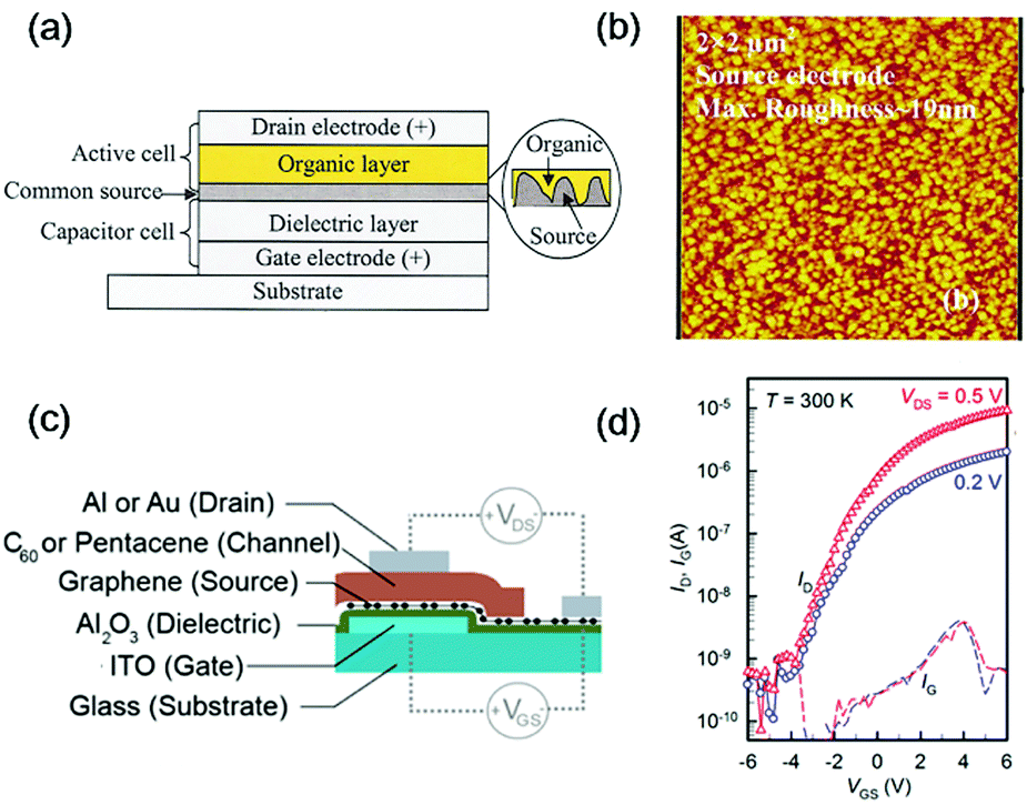 | ||
| Fig. 2 (a) Schematic diagram of the SBVTs with a thermally evaporated Al electrode. (b) Atomic force microscopy image of the surface of the semi-continuous source electrode.48 Copyright 2004, American Institute of Physics. (c) Schematic diagram of a SBVT device comprising a graphene source electrode. (d) Transfer characteristics of a continuous graphene-based SBVTs measured at VDS values of 0.2 and 0.5 V.27 Copyright 2015, American Chemical Society. | ||
To overcome the problems associated to the poor reproducibility and control over the complex morphology of porous electrodes produced by simple thermal evaporation,49 various other techniques have been employed to fabricate porous structures, such as mesh-electrode patterning by a lithographic process,30,50 solution processing of metallic nanowires31,51 and graphene etching.29 Continuous (pore-free) graphene electrodes were also demonstrated as newly emerging source electrodes for SBVTs.52–54 Hlaing et al. have reported a high-performance continuous graphene-based SBVTs (Fig. 2c).27 Upon using a 140-nm-thick layer of C60 as channel layer, the device can be fully turned on and off with a source–drain voltage (VDS) of 0.2 V (Fig. 2d). When a VGS of ±6 V was applied, an Ion/Ioff ratio exceeding 104 and an on-state current density of 44 mA cm−2 were reached.
Moreover, both porous source electrodes and continuous graphene are semi-transparent, allowing the visible light to irradiate towards the OSC layer, enabling the potential use of SBVTs in light–matter interaction studies and applications.
2.2. Metal–insulator–semiconductor type vertical transistors (MISVTs)
MISVTs can differ from lateral transistors by the presence of an additional insulating layer coating the source electrode (Fig. 3a). By taking advantage of the existence of such insulating layer blocking the leakage current through the dielectric encapsulation of the source electrode, the drain electrode can then be stacked on the top of the other layers without the need of being aligned. Hence, the distance between drain and source electrodes directly scales with the thickness of the OSC layer. Kleemann et al. developed high-performance MISVTs with a vertical channel length down to 50 nm via standard photolithography, as shown in Fig. 3a and b. The scanning electron microscopy (SEM) image in Fig. 3c illustrates the topography of the device, composed of a source Au electrode on a 150 nm SiO2 layer covered by a 50 nm C60 layer and the 30 nm Au drain electrode. In this study, MISVTs exhibited high Ion/Ioff ratios of ∼106 and high transconductance values exceeding 50 μS mm−1. Furthermore, when utilizing pentacene as OSC channel layer, on-state current densities of about 50 mA cm−2 were also reached.32 | ||
| Fig. 3 (a) Schematic, (b) microscopic image, and (c) SEM image of a MISVTs fabricated by Kleemann et al.32 Copyright 2013, Wiley-VCH. (d) Three different configurations of the MISVTs. In Device I, the OSC is neither above nor below the source electrode. In Device II, the OSC is placed between the source insulator and the source electrode. In Device III, the OSC is placed in-between the source electrode and the gate insulator. QI, QI′, QII, and QIII represent current pathways in these MISVTs structures, as indicated in the device schematics. (e and f) The current density distributions of device II and device III in the off and in the on state, respectively. In the color code used for the simulations the charges density increases from purple (0) to red (max).55 Copyright 2017, American Institute of Physics. | ||
In this kind of architectures, the position of the source electrode and its coating dielectric layer was found to significantly influence the device performance. Lee et al. have systematically studied three similar MISVTs, as displayed in Fig. 3d.55 For the case of device I, the charges are injected from the side of the source electrode, which was referred to as QI, and then transported towards the drain electrode through the OSC bulk rather than through the gate insulator/OSC interface, resulting in a limited Ion/Ioff ratio and a low switching capability.56 For the case of device II, the charges are injected not only from the side of the source electrode (denoted by QI′, similar to QI), but also from the top of the source electrode (denoted by QII). However, the current pathway of QII still not pass through the charge accumulation zone near the gate insulator and results in a similar limitation of the device performance. For device III, the source electrode with an encapsulation layer was placed in the middle and wrapped by the OSC layer. The charges are injected from the bottom of the source electrode (denoted by QIII) towards the interface between OSC and gate insulator. This design strategy dramatically reduced the current leakage through the device that resulted in a higher Ion/Ioff ratio. By using a commercial calculation software, the authors computed numerical simulations of the current flow in device II and device III under off state and on state, as reported in Fig. 3e and f, respectively. In the off state, a substantial amount of the leakage current was observed in device II, while device III was characterized by an almost-zero electric field distribution within the current leakage pathways. Conversely, when a negative gate voltage was applied and the device was in the on state, device III displayed stronger electric fields compared to device II. Correspondingly, a higher Ion/Ioff ratio was obtained in device III, due to the current passing through the gate insulator/OSC interface which was more effectively controlled by the gate voltage. For these reasons, in principle, the architecture of device III holds a greater potential as a transistor for application in display and photodectetor.57
Furthermore, the contact-doping method has been widely used to optimize the device performance. Günther et al. have found that thin injection layers, compared to mixed layers, can greatly improve the transistor performance because of the significant reduction of contact resistance and transfer length.34 Liu et al. have also investigated a heterogeneous doping of drain and source contacts, being able to suppress the direct source–drain leakage current and thus correspondingly improving the device performance in the saturation regime.33
2.3. Space-charge-limited vertical transistors (SCLVTs)
SCLVTs are three-terminal bias-controlled devices which resemble porous-electrode vertically-stacked structures comprising permeable-base transistors and static-induction transistors. Yet, rather than relying on field-effect charge carrier accumulation at the dielectric/semiconductor interface, the control electrodes in SCLVTs are deposited between the injecting electrode (denoted as emitter) and the extraction electrode (denoted as collector, Fig. 4a), resulting in a structure that consists of two Schottky diodes connected back-to-back. As the current injected from the emitter electrode (IBE) can be drained by the base electrode, not all the current is successfully transferred to and collected by the collector electrode (ICE). Hence, the transmission factor α can be defined as the ratio of the transmitted current to the total current injected at the emitter (α = IBE/ICE).58–60 This effective modulation of injected current by an electrical potential applied between emitter and base (VBE) results in the on/off switch of the transistor. | ||
| Fig. 4 (a) Device scheme of a SCLVTs with an electrochemically oxidized permeable base electrode and (b) transfer curves of these SCLVTs under an emitter-collector voltage VCE of 1 V. Ano 1 V, 2 V and 4 V represent the different anodized Al base electrodes with anodizing potentials of 1, 2, and 4 V.37 Copyright 2019, Wiley-VCH. (c) Cross-section scheme of the built-in channels in SCLVTs developed by Guo et al. (d) Al surface in these devices after removing spheres. The inset shows the size distribution of the nanoholes left on the Al film.36 Copyright 2020, Wiley-VCH. (e) Device structure of SCLVTs based on mesoporous alumina templates. (f) AFM image of the porous anodized alumina membranes.39 Copyright 2017, American Chemical Society. | ||
Similarly to SBVTs, in SCLVTs the perforated base electrode is also critical for controlling the potential profile of the vertical channel and, hence, the performance of VTFTs. For SBVTs, a porous electrode is deposited on the insulating layer, often made of inorganic materials displaying a corrosion resistance to many of the most common organic solvents. However, porous base electrodes in SCLVTs need to be filled with OSCs, which is a limiting factor for the fabrication technology.40,61,62 Dollinger et al. presented an in situ method for passivating the oxide film of the base electrode by wet electrochemical anodization. It has been demonstrated that such an anodization process is not affecting the C60 active layer. Excellent Ion/Ioff ratios of 5 × 10⁵ and on-currents exceeding 300 mA cm−2 indicate that the C60 layer still preserves its semiconducting function.37 High α factors of 99.9996% are achieved with this device structure, as shown in Fig. 4b.
Guo et al. demonstrated another method to fabricate porous gate electrodes via metal deposition on an insulating layer and subsequent creation of pinholes via colloidal lithography (see Fig. 4c).36 After spin-coating PMMA on the substrate, self-assembled polystyrene spheres were utilized as a mask for the thermal evaporation of an Al film. Subsequently, the polystyrene spheres were peeled off with a tape and the PMMA without Al coverage was etched out by using a reactive ion etching system with a power of 20 W and a volume ratio of 2![[thin space (1/6-em)]](https://www.rsc.org/images/entities/char_2009.gif) :1 for O2 and Ar. Consequently, pinholes were left in the PMMA/Al layer as it can be observed in TEM image (Fig. 4d).
:1 for O2 and Ar. Consequently, pinholes were left in the PMMA/Al layer as it can be observed in TEM image (Fig. 4d).
To further simplify the technology, Swathi et al.39 employed well-defined and large-area mesoporous Al2O3 templates providing an inherently scalable architecture to implement vertical conduction in solution-processable P3HT channel layers, as shown in Fig. 4e and f. In this structure, anodized Al2O3 membranes presented a uniformly spaced size distribution and a high pore density of about 109 pores per cm2, which is important to obtain a reliable device operation.
The dual-gate vertical transistor consisting of a single thin-film transistor with an additional second gate and second dielectric is an architecture modification that significatively improves the overall figures of merit, such as a steeper sub-threshold slope, an improved carrier mobility, and an increased Ion/Ioff ratio.63–65 The vertical dual-gate SCLTs reported by Guo et al. exhibited excellent electrical properties with a high on-state current density of 1.54 A cm−2 and a large current gain of 9.2 × 10⁵. Simultaneously, power-efficient applications including inverter and NAND/AND logic units were demonstrated by operating single devices at a bias below 2.0 V.66
3. Electronic and photonic applications
From a geometrical perspective, many VOTFTs architectures have been recently explored to overcome the performance limitations of conventional planar optoelectronic devices, which include light-emitting, photosensitive and memory devices.Thanks to their fast charge transfer characteristics originating from the short channel length in VOTFTs, the efficiency of exciton generation and separation in photonic devices is greatly improved when compared to planar OTFTs. In addition, since the electrodes are covering the top of the OSC layer, they offer a protection towards the surrounding environment, which ensures an air-stable operation in both p- and n-type devices. A major challenge for conventional planar OTFTs in flexible devices is that the lateral transport occurring in the bulk of OSC crystallites can be highly affected by bending and stretching stresses, as the charge transport can be significantly suppressed by the presence of cracks or crystal dislocations under mechanical strain. On the contrary, it has been demonstrated that VTFTs exhibit high tolerance to mechanical strain because the vertical charge transport is much less influenced by these cracks or dislocations.67,68
The vertical channel device configuration could be exploited to construct other organic nanostructured optoelectronic devices integrating various hybrid organic/inorganic active materials, towards the emergence of novel photonic technologies. In this section, we highlight the most remarkable results on photonic and electronic devices based on versatile vertical geometries.
3.1. Light-emitting devices
Organic light-emitting transistors have been considered as core elements for the next-generation of active-matrix (AM) displays, as they integrate both the current-switching and the light-emitting functions in a single device.69,70 Vertical organic light-emitting transistors (VOLETs) are attractive because of the conceptually simple fabrication process consisting in depositing a vertical transistor on a light-emitting diode. Compared to the narrow emission zone typical of lateral LETs, the vertically-stacked configuration ensures higher space utilization and aperture ratios. Hole and electron transport layers were necessarily embedded into devices for balancing the charge injection and thus enhance the light luminescence efficiency. According to the type of charge carriers that are preferentially transported, the materials can be divided into hole transporting materials, which include N,N′-bis(naphthalen-1-yl)-N,N′-bis(phenyl)benzidine (NPB), 2,2′,7,7′-tetra(N,N-di-p-tolyl)amino-9,9-spirobifluorene (Spiro-TTB), 1,1-bis[(di-4-tolylamino)phenyl]cyclohexane (TAPC), 1,3-bis(N-carbazolyl)benzene (mCP), MoO3, and electron transporting materials, which include bathophenanthroline (Bphen), tris(2,4,6-trimethyl-3-(pyridin-3-yl)phenyl)borane (3TPYMB), 1,3,5-tri(m-pyridin-3-ylphenyl)benzene (TmPypB), LiF.Xu et al. have successfully performed the fabrication of SBVT-based VOLETs in 2007.28 By exploiting a process similar to standard OLED fabrication, PEDOT:PSS and the light-emitting polymer (LEP) were spin-coated on an ITO substrate (Fig. 5a). Subsequently, a thin Al source electrode (17 nm) was thermally deposited onto the surface of the LEP. According to the cross-sectional transmission electron microscope (TEM) images shown in Fig. 5b, such a source electrode consists of quasi-discontinuous Al grains that allow the OSC film to contact the dielectric layer by ensuring the direct modulation of the gate-controlled interfacial charge injection. Electrical and optical output characteristics of these VOLET devices are plotted in Fig. 5c and d. The same tendency and similar on/off ratios in electrical and optical characteristics provided unambiguous evidence that the gate bias not only controls the current flow but also the light intensity.
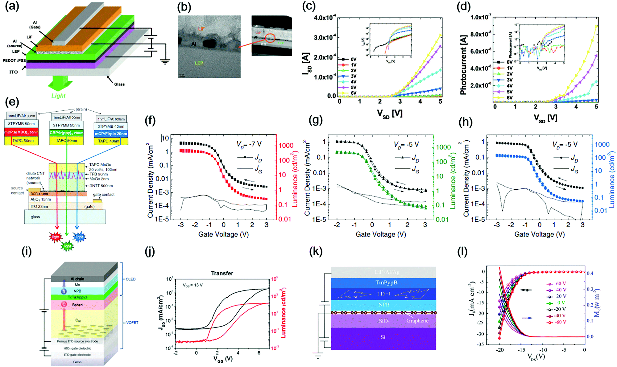 | ||
| Fig. 5 (a) Device structure of the VOLETs based on the SBVT architecture with a porous Al source electrode. (b) Cross-sectional TEM images of these VOLETs indicating the granular structure of the Al film. (c) Electric and (d) optical output characteristics of the same device tested in ambient conditions.28 Copyright 2007, American Institute of Physics. (e) Schematics of the red, green, and blue VOLETs with a single-wall carbon nanotube electrode. Transfer J–L–V curves of the (f) red, (g) green, and (h) blue VOLETs.71 Copyright 2011, American Association for the Advancement of Science. (i) Schematic diagram of the VOLETs with porous ITO electrode. (j) Transfer J–L–V curves of these devices.22 Copyright 2016, American Chemical Society. (k) Schematic image of VOLETs with graphene source electrode. (l) Typical optical and electrical output characteristics of these VOLETs.74 Copyright 2020, American Chemical Society. | ||
Another class of porous electrodes is represented by nanostructured conductors, which includes carbon nanotubes and metal nanowires. McCarthy et al. have reported red, green, and blue VOLETs using single-wall carbon nanotubes as source electrodes.71 The carbon nanotubes transferred on the sample are not only forming a dilute network with superior electrical percolation, but they also exhibit a light transmittance exceeding 98% across the whole visible spectrum. A DNTT layer with a thickness of 500 nm was deposited on the carbon nanotube. Such a thick channel layer can eliminate shorting paths from residual particulates in the carbon nanotube source material. The device structure of OLETs is displayed in Fig. 5e whereas Fig. 5f–h show the transfer characteristics of current density and light luminescence for each of the differently colored devices. By applying suitable drain voltages (VDS) for each VOLETs (−6.8 V for red, −4.9 V for green and −5.7 V for blue), the devices were operated at a gate voltage (VGS) ranging from −3 V to +3 V. All these devices exhibit a maximum luminance around 500 cd m−2 and on/off ratios attaining 104. Similarly to single-wall carbon nanotubes, spin-coated Ag nanowires have been also employed as source electrodes to fabricate VOLETs.72,73
Since a fine control of the source electrode porosity is essential for a homogeneous potential distribution within the channel layer at equilibrium, Yu et al. exploited the self-assembly of polystyrene (PS) nano-spheres to produce a close-packed nanopore array serving as a shadow mask for evaporating the ITO film.22 By controlling the particle size of PS nanospheres by reactive ion etching, the pore size in the ITO film can be tuned from 40 to 150 nm. Based on the optimized VOTFT structure, the authors fabricated VOLETs with the structure illustrated in Fig. 5i. Transfer characteristics were collected at a constant VDS of 13 V. Without gate biasing, the electron injection at the ITO source electrode is negligible, resulting in poor luminance although holes are efficiently injected from the Al drain electrode. At a positive gate bias, the decreased Schottky barrier reflects the increased injection of electrons which then recombine with holes delivering a device luminance of 170 cd m−2 and a high luminance on/off ratio of 104 at VGS = 6 V.
In recent years, graphene-based electrodes have been exploited in VTFTs by taking advantage of the excellent optoelectronic properties of graphene. Liu et al. designed and synthesized an organic molecule, 2,7-diphenyl-9H-fluorene (LD-1), characterized by an intense deep-blue emission. VOLETs based on LD-1 and a graphene gate were fabricated on Si/SiO2 substrates with the structure displayed in Fig. 5k. As illustrated in Fig. 5l, the output characteristics of these OLETs revealed the good electrical and light-emitting tunability under gate bias. When a VDS of −20 V and a VGS of −60 V were applied on devices, a current density of 32 mA cm−2 and a light output power of 0.45 W m−2 were obtained. A uniform and strong blue electroluminescence was also observed on the overall active region.74
MISVTs have also been employed for the fabrication of VOLETs since 2006 by Nakamura et al.75 The architecture is a modified top-contact transistor, where an OLED is stacked on top of a pentacene transistor. One additional insulating layer is deposited on the source electrode so that hole carriers can be injected into the emitting layer by first passing through the OSC channel layer. At negative voltages, hole carriers accumulate in the OSC which acts as anode of the OLED, while the drain electrode act as cathode. When a VDS of −10 V and a VGS of −50 V were applied, a maximum current density of 13.8 mA cm−2 and a luminescence of 290 cd m−2 were recorded, but a poor on/off ratio arised due to the current leakage through the edge of SiO2 insulating layer. To address this problem, Greenman et al. modified the MISVTs-based OLET by covering the edge of the source electrode with an insulator.76 However, the performance of these VOLETs was still not satisfactory considering the requirements for solid-state lighting and active-matrix display applications, because of the complex building technology and an insufficient current density. The current challenges in such VOLET fabrication are thus the following: (i) obtaining a more effective coverage of the insulating layer on the source electrode is sought after for decreasing the leakage current. (ii) Shrinking the size of single devices: according to the theoretical calculations shown in Fig. 3f, the region of high current density (red) is located only nearby the source electrode, for a spatial extension smaller than 1 μm.55 With either shadow mask or photolithography methods, the spacing between the two components of the source electrode was around 50 μm. This distance must be decreased to improve the current density of future VOLETs with the aid of more advanced colloidal lithography and nano-patterning technologies.
Compared to SBVTs and MISVTs, SCLVTs display the unique advantage of combining low operating voltages and high operating speeds.59,77–79 By incorporating a SCLVTs and an OLED into a single device, Wu et al. demonstrated an OLET with a permeable base emitting the three primary colors.80 A schematic cross-section of the VOLET structure indicating the material used for each primary color is depicted in Fig. 6a, where the emitter is a grounded Al electrode, the base (Al/AlOx) and collector (MoOx Au/Ag) electrodes are biased relative to the electrical ground, Bphen/Bphen:Cs and mCP/Spiro-TFB:F6TCNNQ are the electron and the hole transport layers, respectively. After exposing the Al film to ambient air in the dark, the native oxide layer was obtained around the Al electrode as insulating layer. Homogeneously distributed pinholes were also formed in the Al film due to the strain shrinkage, allowing the current from the collector to flow through the base electrode and thus being key for the correct functioning of the device. The transfer characteristics for red, green and blue VOLETs are shown in Fig. 6b–d, respectively. With red, green and blue light emitting materials, peak external quantum efficiencies of 19.6%, 24.6% and 11.8%, and maximum luminance values of 9.833 × 10³ cd m−2, 12.513 × 10³ cd m−2 and 4.753 × 10³ cd m−2 were approached. Due to an effective insulating ability of the self-passivating AlOx layer, high transmission factors were also achieved. The current density of the collector remained above the leakage current density of the base by four orders of magnitude in the on state (base-emitter voltage of 2 V) and by two orders of magnitude in the off state (base-emitter voltage of 0 V). In particular, all VOLETs work at a maximum base-emitter voltage of 3 V and a maximum collector-emitter voltage of 5 V, which paves the way towards efficient and low-voltage OLETs for energy-saving displays.
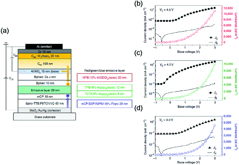 | ||
| Fig. 6 (a) Schematic device structure and hole/electron injection paths of VOLETs based on SCLVTs. For each device color, only the material in light emissive layer is different, ranging from red, green and blue phosphorescent materials. Transfer J–L–V curves of the (b) red, (c) green and (d) blue VOLETs.80 Copyright 2021, Springer Nature. | ||
3.2. Photodetector
Phototransistors show higher photosensitivity and lower noise compared to traditional photodiodes due to their operation mechanism that involves the application of a gate electric field. Hence, they hold great potential for applications in industrial detection, intelligent remote sensing, and optical imaging.81By simple mechanical transfer, a p-type 2,6-diphenyl anthracene (DPA) single crystal has been utilized as channel layer for vertical transistors by Liu et al.82 DPA was chosen as active material because of its high mobility and large Schottky barrier when coupled with graphene, which promotes the decrease of the off-state current. The device architecture of organic single-crystal vertical transistor is reported in Fig. 7a and b. In these phototransistors, the concentration of holes increases when light is irradiated on the DPA single crystal, consequently reducing the Schottky barrier height at the graphene–DPA interface and therefore augmenting the source–drain current (Fig. 7c). Fig. 7d displays the transfer curves of DPA single-crystal vertical phototransistors in dark and under light illumination with different intensities. As the intensity of irradiated light increases, the threshold voltage of the transistors shifts to more positive values. At VGS = 19 V under a light intensity of 2.03 mW cm−2, a high photocurrent of 2 × 10⁻⁷ A and a high ILight/IDark = 104 were obtained. Furthermore, at VGS = 10 V under an illumination intensity of 0.62 mW cm−2, a maximum detectivity (D*) of 1013 Jones was reached. The authors attributed this excellent optoelectronic performance both to the high-quality DPA/source electrode interface and to the high-quality and superior mobility of DPA single crystals having an appropriate Schottky barrier when coupled with graphene and a deep highest occupied molecular orbital (HOMO) energy of −5.6 eV.
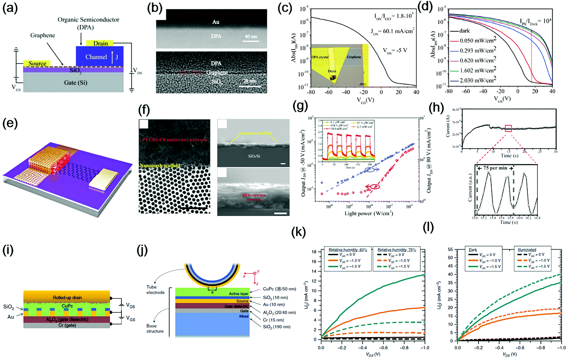 | ||
| Fig. 7 (a) Scheme of the cross-sectional view of the device with graphene and top gold stamp functioning as the source and drain electrodes and DPA single crystal as the vertical channel. (b) High-resolution TEM images of DPA/Au and graphene/DPA interfaces. (c) Typical transfer characteristics of a representative DPA-based VTFT. (d) Transfer characteristics of phototransistors under various illumination intensities compared to that in darkness.82 Copyright 2018, Wiley-VCH. (e) Scheme of VTFTs architecture based on the Au nanomesh scaffold. (f) SEM image of nanomesh electrodes covering the PTCDI-C8 nanowires network. (g) Photocurrent density value at VGS = −50 V (red dots) and VGS = 80 V (blue dots) plotted against different irradiances at 850 nm. Inset: The photoswitching cycles at 850 nm driven by VDS = 20 V and VGS = 60 V. (h) Long-term measurement of the pulse signal measured from vertical phototransistors at resting conditions.83 Copyright 2021, Springer Nature. (i) Front-view and (j) side-view of schematic cross-section of rolled-up NM-based MISVTs. (k) Output curves of rolled-up NM-based MISVTs performed at different humidity levels. (l) Output curves of rolled-up NM-based MISVTs performed in dark and illuminated environments.84 Copyright 2020, Springer Nature. | ||
Near infrared (NIR) organic photodetectors based on wide-bandgap crystalline supramolecular nanowires have been recently reported by our group.83 A novel vertical field-effect phototransistor in which a network of PTCDI-C8 supramolecular nanowires (thickness: ∼900 nm) is sandwiched between a CVD graphene bottom contact and a Au nanomesh top electrode (Fig. 7e). The PTCDI-C8 devices exhibit an impressive photoresponsivity of 2 × 10⁵ A W−1 and 1 × 10² A W−1, at 570 nm and 940 nm, respectively, combined with a photoresponse time as fast as ∼10 ms. We have shown for the first time that a wide bandgap organic prototypical semiconductor, PTCDI-C8 can provide a markedly high light response not only in the visible region of the electromagnetic spectrum, but also in the NIR. Such unique optoelectronic characteristics are the result of an ad hoc supramolecular self-assembly ensuring efficient charge transfer, which determines the emergence of a tailing peak in the absorption spectrum in the NIR region. Real-time heart rate monitoring was also demonstrated hence providing clear evidence of the huge potential of the supramolecular photodetectors for a practical application as a highly efficient photodetection platform.
To the best of our knowledge, only one work has been hitherto published on MISVTs phototransistors by Nawaz et al.84 The authors presented a vertical transistor with multi-sensing capability where the drain electrode is based on rolled-up metallic nanomembranes (NM) with a diameter of ∼8 μm and a source electrode patterned via lithography. A cross-sectional scheme of the front and side-views of these transistors, with copper phthalocyanine (CuPc) operating as active material, is displayed in Fig. 7i. Top drain electrodes based on rolled-up NMs offer an opportunity for a direct interaction between the OSC layer and environmental water molecules. The electrical response of the VOFET devices was recorded under different humidity conditions (60% and 75%), as shown in Fig. 7k. The devices showed a significant decrease in drain-source current density (JDS) when the relative humidity was increased from 60 to 75%, indicating that the adsorption of water molecules on the CuPc layer results in the possible formation of charge traps in the OSC bulk or at the transistor interfacial regions. A second functionality besides the humidity sensing is the light responsivity, as a slight increase in JDS (attributed to the formation of photogenerated electron–hole pairs in the OSC layer) could be observed under exposure to solar light with optical power of 150 W (Fig. 7l). At VDS = −1 V and VGS = −1.5 V, the responsivity and detectivity of the devices approached ∼0.05 A W−1 and ∼109 Jones, respectively.
3.3. Volatile and non-volatile memory devices
The versatility of OSC materials allowed OTFTs to emerge as low-cost and high-performance memory devices facilitating the commercialization of the next-generation of flexible radio-frequency identification tags, integrated circuits and portable electronics.85 An emblematic example is the one of vertical non-volatile memory transistors combining floating gates with chargeable electrets fabricated on flexible substrates.86The unique MISVTs architecture is utilized for memory applications (She et al.).87 It incorporates a down-scaled gate modulation, fast ambipolar accumulation, and quasi-unipolar transport to achieve a significant improvement in the switching speed. By contributing to minimize the charging delays in a relatively long channel and avoiding slow minority carrier accumulation, these chargeable-electrode VTFTs offer a route to realize fast chargeable-gate systems that could meet the industry requirements for data programming (150 ns, P) and erasing (50 ns, E). After a positive gate voltage pulse for programming, carriers accumulate at the DPP-DTT/insulating layer interface and are then injected into the poly(2-vinylnaphthalene) (PVN) electret, resulting in a positive threshold voltage (VTh) shift. For erasing the device memory, a negative gate voltage pulse was then applied, as shown in Fig. 8a and b. A typical memory transfer loop is shown in Fig. 8c. A large anticlockwise hysteresis indicates that the considerable VTh shifts result in a large memory window (ΔVTh). In particular, the writing time dependence of the memory window (Fig. 8d) after applying a writing pulse with different pulse duration was investigated. It was observed that when the writing time exceeded about 1 μs, the ΔVTh had the tendency to saturate, possibly because of the limited charging capability of the polymer.
 | ||
| Fig. 8 Schematic illustrations of different phases of (a) programming and (b) erasing process in chargeable-electrode VTFTs. (c) Memory transfer loop of chargeable-electrode VTFTs. (d) Shift of VTh in the transfer curve of chargeable-electrode VTFTs after 150 ns programming and 50 ns erasing.87 Copyright 2017, Wiley-VCH. (e) Schematic diagram of the device architecture of floating-gate VTFTs. (f) Optical image of a flexible memory device fabricated on the PI substrate. (g) Transfer characteristic curves of floating-gate VTFTs as a function of pulse time. (h) Corresponding memory window variations of the floating-gate VTFTs as a function of pulse time.89 Copyright 2017, Wiley-VCH. | ||
The floating gate organic transistor memory, which resembles a chargeable electrode for its working operation, has also achieved tremendous success as a non-volatile memory device because of its unique advantages, which include non-destructive reading, a sophisticated data-storage mechanism, a reliable long-term data retention capacity, a ultrahigh storage density, and an easy compatibility with integrated circuits.88 Hu et al. reported a flexible photonic memory VTFT by inserting a floating gate into SBVTs.89 A mixed solution of poly(4-vinylphenol) (PVP) and CdSe/ZnS quantum dots (QD) was spin-coated on a Al2O3 dielectric which acts as floating gate for adjusting the Schottky barrier between (HOMO) energy level of PDVT-8 and the work function of Ag nanowires. To explore the programmable and erasable properties of floating-gate VTFTs, the transfer characteristic curves were measured at increasing programming pulse times (Fig. 8g). Longer pulse times induce the formation of more charge carriers which can tunnel into the floating gate and be finally captured by CdSe, resulting in an enlargement of the ΔVTh, as shown in Fig. 8h.
Volatile memory devices have attracted the attention of researchers due to its possible applications in artificial intelligence and brain-like computing. Chen et al. demonstrated the photonic synaptic devices based on a SBVT structure without using any floating gate or polymer electrode for charge retention.90 By employing single-wall carbon nanotubes (SWCNTs) as a porous electrode deposited on a Si/SiO2 substrate, the perovskite VOTFTs was completed by light harvesting CsPbBr3 quantum dots covered by a PDPP4T channel layer and finally capped by a PEDOT:PSS electrode. By taking advantage of the vertical structure, a low working voltage of 10 μV and an ultra-low power consumption of 1.3 fJ per spike can be achieved providing a promising approach for energy-efficient artificial synaptic simulation and neuromorphic computation.
3.4. Multifunctional devices
The integration of multifunctionality in optoelectronics has been considered as instrumental for smart devices technologies.91 Yu et al. fabricated an infrared-to-visible upconversion device by vertically stacking a visible OLED and an IR photodetector in one single device.92 In this configuration, the porous ITO source electrode of the IR photodetector was fabricated by colloidal lithography and acted as cathode in the OLED. The current passing through the OLED can be modulated by both the incident light and the applied gate voltage. Under a positive gate voltage and no IR light irradiation, electrons accumulated on the surface of C60 and insulation layer, resulting in the bending of energy levels. However, the generated electric field is not sufficiently strong to effectively decrease the Schottky barrier between the ITO porous electrode and C60, regulating the on-state current. With the help of IR light irradiation, this Schottky barrier decreased significantly, leading to on-currents suitable for light emission. These upconversion devices exhibits high sensitivity and speed of response, demonstrating their potential for replacing upconversion materials that typically suffer from stringent molecular design and synthesis requirements.4. Summary and outlook
The remarkable progress made in organic vertical transistors over the past 20 years has played a pivotal role in the development of high-performance electronic and photonic applications such as light-emitting devices, photodetector and memory devices. In this Perspective article, we have highlighted the most remarkable recent studies performed on VOTFTs by outlining the impressive advances obtained in the optimization of porous electrodes as well as the development of novel VOFET architectures by discussing both experimental trials and theoretical calculations in light of their potential applications. It is clear throughout the studies discussed above that the simultaneous development of novel multiple functionalities and an ad hoc architecture for devices is essential to access the optimized OSC properties.In light of the future development of VOFETs, three can be considered the major challenges that deserve a more comprehensive investigation: (i) towards the development of flexible computing electronics, little is known on VOFETs-based logic units (e.g. NAND/AND logic gates and inverters). (ii) To improve the current density level of VOFETs, especially for MISVTs structures, the deposition of nanoporous electrodes with large-scale and homogenous hole arrays is necessary. Nanopatterning technologies including electron beam lithography, interference lithography, nanoimprint lithography will enable the fabrication of high-resolution patterned nanostructures for VOFETs. (iii) As of the increasing demand of smart health monitoring, multi-functional sensing devices responding to not only to physical inputs (light, heat and pressure) but also to chemical inputs (ions and gases) require the incorporation of stimuli-responsive molecules in low-power consumption devices.93
In the near future, there are two main hot topics which will attract the attention of researchers: (i) further steps forward when targeting advanced design of the device architecture can be accomplished by exploiting dual-gate VOTFTs and by taking advantage of the threshold voltage setting as a function of the fourth electrode bias, being instrumental for applications in logic gates and integrated circuits. Moreover, dual-gate VOTFTs offer an exquisite control over the recombination zone by integrating the device with an ambipolar OSC or a p–i–n organic junction thereby enabling the balance of hole and electron carrier concentration by choosing appropriate biases to attain high-efficiency electroluminescence for OLED applications.94,95 Hence, vertical dual-gate SBVTs and MISVTs will surely attract a great interest in the scientific community. (ii) In the view of practical applications, multifunctional devices exhibit a great potential for the development of smart devices. Such multifunctional nature can be achieved by manipulating matter via its controlled interaction with the vacuum field by using strategies being developed in the emerging field of light-matter strong coupling,96,97 by increasing the functional complexity in opto-electronic devices and by combining components that are able to impart a distinct function to the ensemble, for example through the integration of both light-emission and memory functions. In this framework, non-volatile light-emitting device and long afterglow light-emitting device were successfully demonstrated by our group via embedding photochromic molecules and metal oxides exhibiting persistent photoconductivity, respectively.98,99 By mastering such a hybrid approach, the fabrication multifunctional devices with short vertical channels will lay the foundations for new emerging optoelectronic devices for memory displays and visual sensors.
Conflicts of interest
There are no conflicts to declare.Acknowledgements
This work was financially supported by the Chinese Scholarship Council and by the European Union's Horizon 2020 research and innovation programme under the Marie Skłodowska-Curie grant agreements No. 811284 (UHMob), the ERC Advanced Grant SUPRA2DMAT (GA-833707) and the Graphene Flagship Core 3 project (GA-881603), the Agence Nationale de la Recherche through the Labex project CSC (ANR-10-LABX-0026 CSC) within the Investissement d’Avenir program (ANR-10-120 IDEX-0002-02), the International Center for Frontier Research in Chemistry (icFRC) and the Institut Universitaire de France (IUF).References
- Y. Zhao, L. Liu, F. Zhang, C. A. Di and D. Zhu, SmartMat., 2021 DOI:10.1002/smm2.1034.
- Y. Yan, Y. Zhao and Y. Liu, J. Polym. Sci., 2021 DOI:10.1002/pol.20210457.
- H. Sirringhaus, Adv. Mater., 2014, 26, 1319–1335 CrossRef CAS PubMed.
- C. D. Dimitrakopoulos and P. R. L. Malenfant, Adv. Mater., 2002, 14, 99–117 CrossRef CAS.
- A. F. Paterson, S. Singh, K. J. Fallon, T. Hodsden, Y. Han, B. C. Schroeder, H. Bronstein, M. Heeney, I. McCulloch and T. D. Anthopoulos, Adv. Mater., 2018, 30, 1801079 CrossRef PubMed.
- Y. Ni, Y. Wang and W. Xu, Small, 2021, 17, 1905332 CrossRef CAS PubMed.
- Q. Zhang, T. Jin, X. Ye, D. Geng, W. Chen and W. Hu, Adv. Funct. Mater., 2021, 2106151, DOI:10.1002/adfm.202106151.
- J. Wang, D. Ye, Q. Meng, C. A. Di and D. Zhu, Adv. Mater. Technol, 2020, 5, 2000218 CrossRef CAS.
- T. Someya, Z. Bao and G. G. Malliaras, Nature, 2016, 540, 379–385 CrossRef CAS PubMed.
- W. Shi, Y. Guo and Y. Liu, Adv. Mater., 2020, 32, 1901493 CrossRef CAS.
- S. Inal, J. Rivnay, A. O. Suiu, G. G. Malliaras and I. McCulloch, Acc. Chem. Res., 2018, 51, 1368–1376 CrossRef CAS PubMed.
- K. Ditte, T. A. Nguyen Le, O. Ditzer, D. I. Sandoval Bojorquez, S. Chae, M. Bachmann, L. Baraban and F. Lissel, ACS Biomater. Sci. Eng., 2021 DOI:10.1021/acsbiomaterials.1c00727.
- H. Liu, A. Yang, J. Song, N. Wang, P. Lam, Y. Li, H. K.-W. Law and F. Yan, Sci. Adv., 2021, 7, eabg8387 CrossRef CAS PubMed.
- Z. Li, S. K. Sinha, G. M. Treich, Y. Wang, Q. Yang, A. A. Deshmukh, G. A. Sotzing and Y. Cao, J. Mater. Chem. C, 2020, 8, 5662–5667 RSC.
- A. C. Arias, J. D. MacKenzie, I. McCulloch, J. Rivnay and A. Salleo, Chem. Rev., 2010, 110, 3–24 CrossRef CAS PubMed.
- L. Zheng, J. Li, K. Zhou, X. Yu, X. Zhang, H. Dong and W. Hu, Nano Res., 2020, 13, 1976–1981 CrossRef CAS.
- S. Griggs, A. Marks, H. Bristow and I. McCulloch, J. Mater. Chem. C, 2021, 9, 8099–8128 RSC.
- X. Guo, M. Baumgarten and K. Müllen, Prog. Polym. Sci., 2013, 38, 1832–1908 CrossRef CAS.
- G. Schweicher, G. Garbay, R. Jouclas, F. Vibert, F. Devaux and Y. H. Geerts, Adv. Mater., 2020, 32, 1905909 CrossRef CAS PubMed.
- U. Zschieschang, J. W. Borchert, M. Giorgio, M. Caironi, F. Letzkus, J. N. Burghartz, U. Waizmann, J. Weis, S. Ludwigs and H. Klauk, Adv. Funct. Mater., 2019, 30, 1903812 CrossRef.
- Y. Yao, L. Zhang, E. Orgiu and P. Samorì, Adv. Mater., 2019, 31, 1900599 CrossRef PubMed.
- H. Yu, Z. Dong, J. Guo, D. Kim and F. So, ACS Appl. Mater. Interfaces, 2016, 8, 10430–10435 CrossRef CAS PubMed.
- G. Han, S. Cao, Q. Yang, W. Yang, T. Guo and H. Chen, ACS Appl. Mater. Interfaces, 2018, 10, 40631–40640 CrossRef CAS.
- M. A. McCarthy, B. Liu, R. Jayaraman, S. M. Gilbert, D. Y. Kim, F. So and A. G. Rinzler, ACS Nano, 2011, 5, 291–298 CrossRef CAS.
- J. Liu, Z. Qin, H. Gao, H. Dong, J. Zhu and W. Hu, Adv. Funct. Mater., 2019, 29, 1808453 CrossRef.
- H. Kleemann, K. Krechan, A. Fischer and K. Leo, Adv. Funct. Mater., 2020, 30, 1907113 CrossRef CAS.
- H. Hlaing, C. H. Kim, F. Carta, C. Y. Nam, R. A. Barton, N. Petrone, J. Hone and I. Kymissis, Nano Lett., 2015, 15, 69–74 CrossRef CAS PubMed.
- Z. Xu, S.-H. Li, L. Ma, G. Li and Y. Yang, Appl. Phys. Lett., 2007, 91, 092911 CrossRef.
- M. G. Lemaitre, E. P. Donoghue, M. A. McCarthy, B. Liu, S. Tongay, B. Gila, P. Kumar, R. K. Singh, B. R. Appleton and A. G. Rinzler, ACS Nano, 2012, 6, 9095–9102 CrossRef CAS PubMed.
- A. J. Ben-Sasson and N. Tessler, Nano Lett., 2012, 12, 4729–4733 CrossRef CAS PubMed.
- X. Qiu, J. Guo, P. A. Chen, K. Chen, Y. Liu, C. Ma, H. Chen and Y. Hu, Small, 2021, 17, 2101325 CrossRef CAS PubMed.
- H. Kleemann, A. A. Gunther, K. Leo and B. Lussem, Small, 2013, 9, 3670–3677 CrossRef CAS.
- S. Liu, M. L. Tietze, A. Al-Shadeedi, V. Kaphle, C. Keum and B. Lüssem, ACS Appl. Electron. Mater., 2019, 1, 1506–1516 CrossRef CAS.
- A. A. Günther, M. Sawatzki, P. Formánek, D. Kasemann and K. Leo, Adv. Funct. Mater., 2015, 26, 768–775 CrossRef.
- H. Kwon, M. Kim, H. Cho, H. Moon, J. Lee and S. Yoo, Adv. Funct. Mater., 2016, 26, 6888–6895 CrossRef CAS.
- E. Guo, S. Xing, F. Dollinger, Z. Wu, A. Tahn, M. Löffler, K. Leo and H. Kleemann, Adv. Mater. Technol., 2020, 5, 2000361 CrossRef CAS.
- F. Dollinger, K. G. Lim, Y. Li, E. Guo, P. Formanek, R. Hubner, A. Fischer, H. Kleemann and K. Leo, Adv. Mater., 2019, 31, 1900917 CrossRef PubMed.
- A. Fischer, R. Scholz, K. Leo and B. Lüssem, Appl. Phys. Lett., 2012, 101, 213303 CrossRef.
- K. Swathi and K. S. Narayan, Nano Lett., 2017, 17, 7945–7950 CrossRef CAS PubMed.
- Y. M. Chen, Y. Y. Lai, Y. C. Chao, H. W. Zan, H. F. Meng, S. F. Horng and C. H. Chang, ACS Appl. Mater. Interfaces, 2015, 7, 18899–18903 CrossRef CAS.
- Y. Liu, J. Guo, E. Zhu, P. Wang, V. Gambin, Y. Huang and X. Duan, ACS Nano, 2019, 13, 847–854 CrossRef CAS PubMed.
- N. Stutzmann, R. H. Friend and H. Sirringhaus, Science, 2003, 299, 1881–1884 CrossRef CAS PubMed.
- J. Lenz, F. Del Giudice, F. R. Geisenhof, F. Winterer and R. T. Weitz, Nat. Nanotechnol., 2019, 14, 579–585 CrossRef CAS PubMed.
- J. Lenz, A. M. Seiler, F. R. Geisenhof, F. Winterer, K. Watanabe, T. Taniguchi and R. T. Weitz, Nano Lett., 2021, 21, 4430–4436 CrossRef CAS PubMed.
- Y. Yao, L. Zhang, T. Leydecker and P. Samorì, J. Am. Chem. Soc., 2018, 22, 6984–6990 CrossRef PubMed.
- Y. Li, P. Sonar, L. Murphya and W. Hong, Energy Environ. Sci., 2013, 6, 1684–1710 RSC.
- H. Wang, Y. Wang, Z. Ni, N. Turetta, S. M. Gali, H. Peng, Y. Yao, Y. Chen, I. Janica, D. Beljonne, W. Hu, A. Ciesielski and P. Samorì, Adv. Mater., 2021, 33, 2008215 CrossRef CAS PubMed.
- L. Ma and Y. Yang, Appl. Phys. Lett., 2004, 85, 5084–5086 CrossRef CAS.
- S.-H. Li, Z. Xu, L. Ma, C.-W. Chu and Y. Yang, Appl. Phys. Lett., 2007, 91, 083507 CrossRef.
- H. Yu, Y. Cheng, D. Shin, S.-W. Tsang and F. So, Adv. Electron. Mater., 2018, 4, 1800039 CrossRef.
- X. Song, Y. Zhang, H. Zhang, Y. Yu, M. Cao, Y. Che, J. Wang, H. Dai, J. Yang, X. Ding and J. Yao, Nanotechnology, 2016, 27, 405201 CrossRef PubMed.
- C. Pan, Y. Fu, J. Wang, J. Zeng, G. Su, M. Long, E. Liu, C. Wang, A. Gao, M. Wang, Y. Wang, Z. Wang, S.-J. Liang, R. Huang and F. Miao, Adv. Electron. Mater., 2018, 4, 1700662 CrossRef.
- J. Kang, D. Jariwala, C. R. Ryder, S. A. Wells, Y. Choi, E. Hwang, J. H. Cho, T. J. Marks and M. C. Hersam, Nano Lett., 2016, 16, 2580–2585 CrossRef CAS PubMed.
- M. Kuiri, B. Chakraborty, A. Paul, S. Das, A. K. Sood and A. Das, Appl. Phys. Lett., 2016, 108, 063506 CrossRef.
- G. Lee, I.-H. Lee, H.-L. Park, S.-H. Lee, J. Han, C. Lee, C.-M. Keum and S.-D. Lee, J. Appl. Phys., 2017, 121, 024502 CrossRef.
- C. M. Keum, I. H. Lee, S. H. Lee, G. J. Lee, M. H. Kim and S. D. Lee, Opt. Express, 2014, 22, 14750–14756 CrossRef CAS PubMed.
- G. Sheleg, M. Greenman, B. Lussem and N. Tessler, J. Appl. Phys., 2017, 122, 195502 CrossRef.
- Y. Watanabe and K. Kudo, Appl. Phys. Lett., 2005, 87, 223505 CrossRef.
- F. Pu, Y. Watanabe, H. Yamauchi, M. Nakamura and K. Kudo, Thin Solid Films, 2009, 518, 514–517 CrossRef CAS.
- Y.-C. Chao, C.-Y. Chen, H.-W. Zan and H.-F. Meng, J. Phys. D: Appl. Phys., 2010, 43, 205101 CrossRef.
- P.-Y. Chang, S.-F. Peng, Y.-C. Chao, H.-C. Lin, H.-W. Zan and H.-F. Meng, Appl. Phys. Lett., 2015, 106, 153301 CrossRef.
- H. Li, T. Chen and Y. Chao, Nano Res., 2014, 7, 938–944 CrossRef CAS.
- M. Nikolka, D. Simatos, A. Foudeh, R. Pfattner, I. McCulloch and Z. Bao, ACS Appl. Mater. Interfaces, 2020, 12, 40581–40589 CrossRef CAS PubMed.
- F. Liao, Z. Guo, Y. Wang, Y. Xie, S. Zhang, Y. Sheng, H. Tang, Z. Xu, A. Riaud, P. Zhou, J. Wan, M. S. Fuhrer, X. Jiang, D. W. Zhang, Y. Chai and W. Bao, ACS Appl. Electron. Mater., 2019, 2, 111–119 CrossRef.
- W. S. Roelofs, M. J. Spijkman, S. G. Mathijssen, R. A. Janssen, D. M. de Leeuw and M. Kemerink, Adv. Mater., 2014, 26, 4450–4455 CrossRef CAS PubMed.
- E. Guo, Z. Wu, G. Darbandy, S. Xing, S. J. Wang, A. Tahn, M. Gobel, A. Kloes, K. Leo and H. Kleemann, Nat. Commun., 2020, 11, 4725 CrossRef PubMed.
- Y. Zheng, G. J. N. Wang, J. Kang, M. Nikolka, H. C. Wu, H. Tran, S. Zhang, H. Yan, H. Chen, P. Y. Yuen, J. Mun, R. H. Dauskardt, I. McCulloch, J. B. H. Tok, X. Gu and Z. Bao, Adv. Funct. Mater., 2019, 29, 1905340 CrossRef CAS.
- A. D. Printz and D. J. Lipomi, Appl. Phys. Rev., 2016, 3, 021302 Search PubMed.
- Z. Qin, H. Gao, J. Liu, K. Zhou, J. Li, Y. Dang, L. Huang, H. Deng, X. Zhang, H. Dong and W. Hu, Adv. Mater., 2019, 31, 1903175 CrossRef PubMed.
- L. Ma, D. Qin, Y. Liu and X. Zhan, J. Mater. Chem. C, 2018, 6, 535–540 RSC.
- M. A. McCarthy, B. Liu, E. P. Donoghue, I. Kravchenko, D. Y. Kim, F. So and A. G. Rinzler, Science, 2011, 232, 570–573 CrossRef PubMed.
- M. A. Mohd Sarjidan, A. Shuhaimi and W. H. A. Majid, Curr. Appl. Phys., 2018, 18, 1415–1421 CrossRef.
- Q. Chen, Y. Yan, X. Wu, S. Lan, D. Hu, Y. Fang, D. Lv, J. Zhong, H. Chen and T. Guo, ACS Appl. Mater. Interfaces, 2019, 11, 35888–35895 CrossRef CAS PubMed.
- D. Liu, J. De, H. Gao, S. Ma, Q. Ou, S. Li, Z. Qin, H. Dong, Q. Liao, B. Xu, Q. Peng, Z. Shuai, W. Tian, H. Fu, X. Zhang, Y. Zhen and W. Hu, J. Am. Chem. Soc., 2020, 142, 6332–6339 CrossRef CAS PubMed.
- K. Nakamura, T. Hata, A. Yoshizawa, K. Obata, H. Endo and K. Kudo, Appl. Phys. Lett., 2006, 89, 103525 CrossRef.
- M. Greenman, G. Sheleg, C.-M. Keum, J. Zucker, B. Lussem and N. Tessler, J. Appl. Phys., 2017, 121, 204503 CrossRef.
- D. Yang, S. Yang, L. Zhang, Y. Wang, C. Fu, T. Song, R. Liu and B. Zou, Org. Electron., 2016, 31, 273–277 CrossRef CAS.
- E. Guo, F. Dollinger, B. Amaya, A. Fischer and H. Kleemann, Adv. Opt. Mater., 2021, 9, 2002058 CrossRef CAS.
- G. Darbandy, F. Dollinger, P. Formánek, R. Hübner, S. Resch, C. Roemer, A. Fischer, K. Leo, A. Kloes and H. Kleemann, Adv. Electron. Mater., 2020, 6, 2000230 CrossRef CAS.
- Z. Wu, Y. Liu, E. Guo, G. Darbandy, S. J. Wang, R. Hubner, A. Kloes, H. Kleemann and K. Leo, Nat. Mater., 2021, 20, 1007–1014 CrossRef CAS PubMed.
- Y. Yao, Y. Chen, H. Wang and P. Samorì, SmartMat., 2020, 1, e1009 CrossRef.
- J. Liu, K. Zhou, J. Liu, J. Zhu, Y. Zhen, H. Dong and W. Hu, Adv. Mater., 2018, 30, 1803655 CrossRef PubMed.
- Y. Yao, Q. Ou, K. Wang, H. Peng, F. Fang, Y. Shi, Y. Wang, D. I. Asperilla, Z. Shuai and P. Samorì, Nat. Commun., 2021, 12, 3667 CrossRef CAS PubMed.
- A. Nawaz, L. Merces, D. M. de Andrade, D. H. S. de Camargo and C. C. Bof Bufon, Nat. Commun., 2020, 11, 841 CrossRef CAS PubMed.
- T. Leydecker, M. Herder, E. Pavlica, G. Bratina, S. Hecht, E. Orgiu and P. Samorì, Nat. Nanotechnol., 2016, 11, 769–775 CrossRef CAS PubMed.
- S. T. Han, Y. Zhou and V. A. Roy, Adv. Mater., 2013, 25, 5425–5449 CrossRef CAS PubMed.
- X. J. She, D. Gustafsson and H. Sirringhaus, Adv. Mater., 2017, 29, 1604769 CrossRef PubMed.
- M. Kang, K.-J. Baeg, D. Khim, Y.-Y. Noh and D.-Y. Kim, Adv. Funct. Mater., 2013, 23, 3503–3512 CrossRef CAS.
- D. Hu, X. Wang, H. Chen and T. Guo, Adv. Funct. Mater., 2017, 27, 1703541 CrossRef.
- T. Chen, X. Wang, D. Hao, S. Dai, Q. Ou, J. Zhang and J. Huang, Adv. Opt. Mater., 2021, 9, 2002030 CrossRef CAS.
- E. Orgiu and P. Samorì, Adv. Mater., 2014, 26, 1827–1845 CrossRef CAS PubMed.
- H. Yu, D. Kim, J. Lee, S. Baek, J. Lee, R. Singh and F. So, Nat. Photonics, 2016, 10, 129–134 CrossRef CAS.
- H. Qiu, S. Ippolito, A. Galanti, Z. Liu and P. Samorì, ACS Nano, 2021, 15, 10668–10677 CrossRef PubMed.
- J.-H. Lee, T.-H. Ke, J. Genoe, P. Heremans and C. Rolin, Adv. Electron. Mater., 2019, 5, 1800437 CrossRef.
- B. B. Hsu, C. Duan, E. B. Namdas, A. Gutacker, J. D. Yuen, F. Huang, Y. Cao, G. C. Bazan, I. D. Samuel and A. J. Heeger, Adv. Mater., 2012, 24, 1171–1175 CrossRef CAS PubMed.
- E. Orgiu, J. George, J. A. Hutchison, E. Devaux, J. F. Dayen, B. Doudin, F. Stellaci, C. Genet, J. Schachenmayer, C. Genes, G. Pupillo, P. Samori and T. W. Ebbesen, Nat. Mat., 2015, 14, 1123–1129 CrossRef CAS PubMed.
- F. J. Garcia-Vidal, C. Ciuti and T. W. Ebbesen, Science, 2021, 373, eabd0336 CrossRef CAS PubMed.
- L. Hou, X. Zhang, G. F. Cotella, G. Carnicella, M. Herder, B. M. Schmidt, M. Patzel, S. Hecht, F. Cacialli and P. Samorì, Nat. Nanotechnol., 2019, 14, 347–353 CrossRef CAS PubMed.
- Y. Chen, H. Wang, Y. Yao, Y. Wang, C. Ma and P. Samorì, Adv. Mater., 2021, 33, 2103369 CrossRef CAS PubMed.
| This journal is © The Royal Society of Chemistry 2022 |