 Open Access Article
Perspectives on metal induced crystallization of a-Si and a-Ge thin films
G. Maity
*ab,
S. Dubey
c,
T. Meher
b,
S. Dhar
a,
D. Kanjilal
d,
T. Som
ef and
Shiv P. Patel
 *b
*b
aDepartment of Physics, Shiv Nadar Institute of Eminence, Gautam Buddha Nagar-201314, India. E-mail: gurupada.phy@gmail.com
bDepartment of Pure & Applied Physics, Guru Ghasidas Vishwavidyalaya (A Central University), Bilaspur-495009, India. E-mail: shivpoojanbhola@gmail.com
cApplied Science Cluster, School of Engineering, University of Petroleum & Energy Studies, Bidholi, Dehradun-248007, India. E-mail: santosh.dubey@ddn.upes.ac.in
dInter University Accelerator Centre, Aruna Asaf Ali Marg, New Delhi-110067, India
eInstitute of Physics, Sachivalaya Marg, Bhubaneswar-751005, India
fHomi Bhabha National Institute, Training School Complex, Anushakti Nagar, Mumbai-40008, India
First published on 28th November 2022
Abstract
In recent times, the metal induced crystallization (MIC) process in amorphous semiconductors (a-Si and a-Ge) has been extensively investigated by many researchers due to potential applications of crystalline semiconductors in high-density data storage devices, flat panel displays, and high performance solar cells. In this context, we have presented a review on different schemes of MIC in metal/a-Si and metal/a-Ge bilayer films (with stacking change) on various substrates under different annealing conditions. The parameters, which limit crystallization of a-Si and a-Ge have been analyzed and discussed extensively keeping in mind their applications in solar cells and flat panel displays. The MIC of a-Si and a-Ge films under ion beam irradiation has also been discussed in detail. At the end, some suggestions to overcome the limitations of the MIC process in producing better crystalline semiconductors have been proposed. We believe that this review article will inspire readers to perform a thorough investigation on various aspects of MIC for further development of high efficiency solar cells and high quality flat panel displays.
1. Introduction
It is now evident that silicon (Si) and germanium (Ge) based devices have dominated the microelectronics industry, which may be understood from the fact that more than 90% of the sales in the global semiconductor market account for Si and Ge based devices.1,2 Polycrystalline silicon and germanium (p-Si and p-Ge), in particular, have been found to be suitable materials for high-density data storage devices, thin film transistors and solar cells.3,4 However, due to the production cost of p-Si and p-Ge based solar cells, the cost of electricity production is higher. Therefore, there is an opportunity for the research community to produce low cost p-Si and p-Ge as substrates in solar cells to lower the overall cost of the solar cell production. In order to address the above, significant efforts have been directed towards developing p-Si and p-Ge via solid-phase crystallization (SPC) of amorphous-Si (a-Si) and amorphous-Ge (a-Ge).5,6 However, SPC process suffers from long annealing times even at 600 °C for Si and 550 °C for Ge; these temperatures are too high for large-area glass substrates. Moreover, the bulk amorphous semiconductors crystallize at higher temperatures (500–600 °C).5–7 It has been reported that a-Ge and a-Si crystallize at a very low temperatures when they are in contact with metals such as Al,8–24 Au,25–29 Ag,30–32 Ni,33–40 Cu,41–43 and Pd,44,45 in comparison to their “bulk” crystallization temperatures. This process is called as metal-induced crystallization (MIC), which was first observed 50 years before in the case of a-Ge.46–50 In the last decade, MIC process for different metal/a-semiconductor bilayer systems has been extensively investigated. In this context, we present a detailed review on different MIC schemes to prepare semiconductors films of desired physical properties. The parameters that limit the crystallization of amorphous-semiconductors are discussed in detail; some suggestions for further development of these materials for the solar cell and flat panel display have been proposed. This review should also apprise the readers about the recent developments in developing crystalline semiconductors using MIC process, and equip them with the needed information to develop materials for efficient inorganic solar cells and various other applications of interest.2. Brief history and importance of MIC of a-Ge and a-Si
Oki et al.46 observed in 1969 that the crystallization of a-Ge happens at low temperature in the proximity with some metals such as Au, Al, Ag, Sn or Cu. Bosnel and Voisey51 also reported similar finding in the case of a-Si. Vacuum evaporation scheme was used to prepare samples (amorphous semiconductor + metal layer) and electron diffraction technique was used to investigate the crystallization in both the above studies. The crystallization phenomenon in presence of metals has been named metal-contact-induced crystallization,52 which is also popularly known as MIC. Herd et al.52 and Ottaviani et al.53–55 carried out more extensive electron microscopic investigations on MIC. Based on the observations made in the above investigations, MIC effect was understood to happen broadly in two steps: (1) dissolution of the semiconductor into the metal along the metal/semiconductor interface and (2) precipitation of the semiconductor crystallites out of the metal matrix.53–55 According to Brodsky et al,56 in a bilayer system (where one component is amorphous), MIC proceeds by the development of a eutectic melt produced at low temperature (i.e. binary eutectic temperature). In 1990s, the understanding of MIC process got an impetus with the use of in situ transmission electron microscopy (TEM) techniques. In situ heating high-resolution transmission electron microscopy (HRTEM) was employed to investigate MIC in metal semiconductor eutectic systems, like crystalline Al (c-Al)/a-Si,8 c-Ag/a-Si30 and, c-Ag/a-Ge;57 the results showed it to be a complete solid-state process. Furthermore, in all the observations discussed so far, no metastable metal semiconductor compound was observed during MIC.8,30,57,58 In situ heating HRTEM was also employed to study the MIC process in Ni/a-Si system; in this study, MIC was observed to happen by the formation of solid silicide phase (NiSi2) initially, and its subsequent migration into the a-Si film to form crystalline Si (c-Si) phase.33,59 After 1990s, metal-induced layer exchange (MILE)7,9,10 and metal-induced lateral crystallization (MILC)35,44,60 mechanism were used to explain amorphous to crystalline phase transformation. In these mechanisms, Al and Si sublayers in the c-Al/a-Si system exchange their original positions to form approximately continuous c-Si layer at the original position of the Al sublayer at low temperature.7 During annealing of the bilayer system, the growth of crystalline semiconductor phase was observed both at the metal contacted region as well as laterally outside the metal covered region. The possibility of low temperature synthesis of p-Si and p-Ge makes MILC a very useful scheme to develop thin-film transistors (TFT) and advanced flat panel displays. In 2003, Mittemeijer, explained MIC and MILE processes using interface thermodynamics.11–22,47,61–64 Auger electron spectroscopy (AES) depth profile measurements were used to describe the kinetics of MIC and MILE by quantitatively evaluating inter-diffusion processes in metal/semiconductor layered systems.16,61,62 Recently, a novel advanced real-time in situ analytic TEM technique was proposed to understand the atomic-scale mechanism of MIC and MILE.21,22 With the persistent efforts of the research community since the year 2000 and even before, it has been now possible to develop solar cells having efficiencies more than 8% using c-Si prepared based on Al-induced crystallization.65 A recent success in developing advanced display devices having exceptional performance via low-temperature MILC of a-Si is noteworthy.66 MIC has also been used to develop Blu-ray data storage devices because very low power and low cost laser irradiation is sufficient to attain the needed crystallization temperature in metal/a-Si (or a-Ge) bilayer systems.673. Preparation methods
The amorphous semiconductor (a-Si and a-Ge) thin films can be prepared at low temperatures by two methods: chemical and physical method. Chemical methods such as chemical vapor deposition (CVD), plasma-enhanced chemical vapor deposition (PECVD), and hotwire chemical vapor deposition (HWCVD) are employed to deposit metal/semiconductor layer thin films. Sputtering (direct current sputtering and magnetron sputtering), evaporation (thermal evaporation and electron beam evaporation) and molecular beam epitaxy (MBE) are some of the physical methods employed in the preparation of amorphous semiconductor thin films. In addition to these methods, low energy ion irradiation of crystalline semiconductors may also be used to prepare amorphous semiconductor films.68,69 The microstructure of an amorphous semiconductor and its crystallization behaviors (like crystallization temperature, crystallization energy, etc.) may be very different depending on the fabrication methods.68,70 The existence of hydrogen and doping elements may also influence the crystallization of amorphous semiconductors.70 In the following section, different processes of sample preparation have been summarized.3.1. Chemical methods
Chemical vapor deposition (CVD) is a chemical process, useful for atomic layer deposition. Matsumura et al.71 deposited hydrogenated amorphous silicon (a-Si:H) films using SiH4 and H2 gas mixture without using any plasma or photochemical excitation, but using only thermal and catalytic reactions between deposition-gas and a heated tungsten catalyzer. Wang et al.72 deposited single-crystal germanium nanowires by the CVD of germane (GeH4) at 275 °C with Au nanocrystals as seed particles. Low-pressure chemical vapor deposition (LPCVD) method is used to reduce unwanted gas-phase reaction and improve film uniformity across the substrate. The a-Si films of different thicknesses (i.e. 50–200 nm) were deposited on different substrates (i.e. thermally oxidized Si, glass, and quartz) by LPCVD method at the substrate temperature in the range of 400–600 °C.40,73–79 For example, Miyasaka et al.40 deposited 50 nm a-Si thin films by LPCVD process on glass substrate at 425 °C and 1.1 torr pressure. Pereira et al.74 prepareda-Si thin films (80–125 nm) on a glass substrate by LPCVD method at 550 °C, 30 Pa pressure and with the silane (SiH4) flow of 30 sccm. Ahn et al.75 deposited a-Si (50 nm) on SiO2 by LPCVD method at 450 °C with a deposition pressure of 200 mTorr and disilane (Si2H6) as a source gas for Si. Jung et al.76 deposited 100 nm thick a-Si layer with the help of SiH4 gas (with a pressure of 136 mTorr), at 525–550 °C in a LPCVD system with three different in situ doping conditions. Gardelis group77 deposited a-Si films on quartz substrate at 610 °C with the base pressure of 300 mTorr by LPCVD method. The MIC was then studied by depositing different types of metals (i.e. Ni, Al, etc.) on amorphous semiconductor films deposited by LPCVD and annealing the bilayer samples at low temperatures in the range 450–500 °C.40,73–79 PECVD is also one type of CVD technique used to enhance the rate of chemical reaction at low temperatures. Several researchers have used PECVD technique to prepare a-Si and a-Ge thin films on different substrates.80–85 Haque et al.80 employed an ultra-high vacuum (UHV) PECVD method with the base pressure of 8 × 10⁻⁷ torr at 250 °C (deposition pressure: 500 mTorr, and power density: 50 mW cm−2) to deposit phosphorus-doped a-Si:H films on the oxidized silicon and glass substrates. Choi et al.81 deposited a-Si:H film (50 nm) on glass by PECVD method with a RF power density of 0.27 W cm−2 at a temperature of 270 °C using a 25% silane and 75% hydrogen mixture. Giangregorio et al.82 deposited a-Ge (500 nm) on p-type c-Si (100) by PECVD method using GeH4![[thin space (1/6-em)]](https://www.rsc.org/images/entities/char_2009.gif) :
:![[thin space (1/6-em)]](https://www.rsc.org/images/entities/char_2009.gif) H2 (∼2
H2 (∼2![[thin space (1/6-em)]](https://www.rsc.org/images/entities/char_2009.gif) :
:![[thin space (1/6-em)]](https://www.rsc.org/images/entities/char_2009.gif) 38) mixture at a pressure of 0.28 torr, temperature of 275 °C, and an RF power of 3 W. Schmidt et al.83 employed PECVD method to deposit a-Si on a glass plate using reactant gases like silane (SiH4), phosphine (PH3, forn-type doping) and diborane (B2H6, forp-type doping), without hydrogen dilution at a temperature of 200 °C, at a pressure of 600 μbar and power density of 120 mW cm−2 (frequency 50 MHz). Peng et al.84 used a radio frequency (13.56 MHz) capacitive-coupled PECVD system in Ar and GeH4 (H2 dilution) mixture with a total flow of 20 sccm to deposit a-Ge:H thin films (∼1 μm thickness) on the surface of Al films at 200 °C. The deposition and base pressure were 3.0 × 10⁻⁴ Pa and 150 Pa, respectively. The MIC was studied on PECVD deposited amorphous semiconductor films in contact with different metals by annealing the bilayer systems in the temperature range of 170–300 °C.80–85 The HWCVD is also known as catalytic CVD, is a new technology for depositing amorphous-semiconductors thin films at low temperatures without the use of plasma to decompose source gases.86–88 Ebil et al.86 deposited a-Si film (of 500–1000 nm thickness) by custom mode HWCVD system with load lock (base pressure of 6.67 × 10⁻⁵ Pa) at a filament temperature of 430–1850 °C and deposition pressure of 3.33 Pa; silane was used as the source gas without hydrogen dilution. Chong et al.88 prepared five sets of a-Si samples by HWCVD at different temperatures ranging from 200 to 400 °C with an interval of 50 °C at a chamber base pressure of approximately 2 × 10⁻⁵ mbar. The SiH4 gas flow-rate and deposition pressure were maintained at 5 sccm and 0.18 mbar, respectively. The MIC was observed at temperatures ranging from 200 to 400 °C.86–88
38) mixture at a pressure of 0.28 torr, temperature of 275 °C, and an RF power of 3 W. Schmidt et al.83 employed PECVD method to deposit a-Si on a glass plate using reactant gases like silane (SiH4), phosphine (PH3, forn-type doping) and diborane (B2H6, forp-type doping), without hydrogen dilution at a temperature of 200 °C, at a pressure of 600 μbar and power density of 120 mW cm−2 (frequency 50 MHz). Peng et al.84 used a radio frequency (13.56 MHz) capacitive-coupled PECVD system in Ar and GeH4 (H2 dilution) mixture with a total flow of 20 sccm to deposit a-Ge:H thin films (∼1 μm thickness) on the surface of Al films at 200 °C. The deposition and base pressure were 3.0 × 10⁻⁴ Pa and 150 Pa, respectively. The MIC was studied on PECVD deposited amorphous semiconductor films in contact with different metals by annealing the bilayer systems in the temperature range of 170–300 °C.80–85 The HWCVD is also known as catalytic CVD, is a new technology for depositing amorphous-semiconductors thin films at low temperatures without the use of plasma to decompose source gases.86–88 Ebil et al.86 deposited a-Si film (of 500–1000 nm thickness) by custom mode HWCVD system with load lock (base pressure of 6.67 × 10⁻⁵ Pa) at a filament temperature of 430–1850 °C and deposition pressure of 3.33 Pa; silane was used as the source gas without hydrogen dilution. Chong et al.88 prepared five sets of a-Si samples by HWCVD at different temperatures ranging from 200 to 400 °C with an interval of 50 °C at a chamber base pressure of approximately 2 × 10⁻⁵ mbar. The SiH4 gas flow-rate and deposition pressure were maintained at 5 sccm and 0.18 mbar, respectively. The MIC was observed at temperatures ranging from 200 to 400 °C.86–88
3.2. Physical methods
Sputtering is used to deposit a-semiconductors and metal thin film by sputter out target atom bombarding with ions in a high vacuum chamber.49,89–98 Zanatta et al.89 deposited hydrogenated a-Ge:H and Al films on c-Si substrate by sputtering in a high vacuum (residual pressure ∼3 × 10⁻⁶ mbar, radio frequency ∼13.56 MHz) sputtering system with the substrate held at 220 °C. Wang et al.90 prepared a-Si and Al bilayer system by magnetron sputtering in a high vacuum chamber. Muniz et al.91 deposited a-Ge:H(Al) samples onto polished (air-exposed) crystalline silicon (111) and Corning 7059 glass substrates kept at 220 °C in a high-vacuum radio frequency (RF) sputtering system using argon as the sputtering gas. Knaepen et al.49 deposited a-Si (200 nm) and Al (30 nm) layer system by RF sputtering at room temperature on thermally grown SiO2 (100 nm) with the deposition pressure of 10−4 Pa. Kezzoula et al.93 deposited a-Si and a-Si:H on Al/glass and glass substrate using DC magnetron sputtering at 250 °C with the input power of 100 W (power density 2.25 W cm−2). Toko et al.95 deposited Al and a-Ge thin films each of thickness 50 nm on quartz (SiO2) by RF sputtering at room temperature. Ou et al.96 prepared a-Ge and Ni layer system on SiO2 glass and polycarbonate substrate at room temperature by sputtering (input power 50 W) with a deposition pressure of 0.67 Pa. Chen et al.98 deposited Al and a-Si film on quartz substrate using a RF magnetron sputtering apparatus with a deposition rate of 17.4 nm min−1 and 19.4 nm min−1, respectively. Evaporation is a common physical vapor deposition (PVD) method to form uniform thin films. There are two types of evaporation methods: thermal and electron beam. Thermal evaporation is suitable for low melting point materials (such as metals), whereas s electron-beam (e-beam) evaporation is suitable for high melting point materials (such as semiconductors).50,99–107 Katsuki et al.99 deposited Al (134 nm)/a-Ge (108 nm) on SiO2 by vacuum evaporation at the room temperature with a base pressure of 104 Pa. Alford et al.100 used e-beam evaporation to deposit a-Si (800 nm)/Al (20 nm) on thermally oxidized SiO2 (200 nm) at room temperature with the base pressure of 3 × 10⁻⁶ torr. Knaepen et al.50 prepared a-Ge (200 nm) and 20 transition metals (Ti, Zr, Hf, V, Nb, Ta, Cr, Mo, W, Mn, Re, Fe, Ru, Co, Rh, Ir, Ni, Pd, Pt, Cu, Ag, Au, and Al) layer system with a thickness of 30 nm by e-beam evaporation at a base pressure of 10−4 Pa. Hu et al.101 deposited a-Ge (100 nm) and Al (50 nm) layer system on fussed silica (SiO2) by e-beam evaporation at room temperature. Takiguchi et al.102 deposited a-Si/Au and a-Ge/Au layer system by e-beam evaporation on sapphire at room temperature and chamber pressure of 5 × 10⁻⁶ Pa. Mohiddon et al.103 deposited a 500 nm a-Si film followed by a 200 nm Ni film by e-beam evaporation on borosilicate glass substrate with the deposition pressure of 5 × 10⁻⁶ torr at room temperature. Karaman et al.105 deposited 15 nm Au film onto Al-doped ZnO (AZO) film by e-beam evaporation and after the formation of Au nano particles, 1 μm of a-Si layer was deposited on Au/AZO bilayer system at 200 °C with a vacuum of 5 × 10⁻⁷ torr. The crystallization of a-semiconductor thin films deposited by sputtering was then studied by annealing of metal/a-semiconductor systems at the temperature range of 160–600 °C in different atmosphere.49,89–98 Molecular beam epitaxy (MBE) has also been used to prepare a-semiconductors thin films.108–111 Sadoh et al.108 deposited a-Ge layers (100 nm thick) on the SiO2 films (160 nm) using MBE technique (base pressure: 5 × 10⁻¹⁰ torr) at room temperature. Uenuma et al.109 deposited a-Ge films with the thickness of 30 nm on SiO2 (100 nm)/Si substrates by MBE technique. Park et al.110 deposited Au films (thickness: 100 nm) on quartz substrates at room temperature by electron beam evaporation. After sputter deposited Al2O3 (0–10 nm), the a-Ge films (thickness: 100 nm) were deposited using the MBE system. Ooato et al.111 prepared Sn films and a-Ge films each of 100 nm thickness on quartz substrate at room temperature by MBE technique (base pressure: ∼7 × 10⁻⁸ Pa, deposition rate: 0.01 nm s−1). Metal induced lateral crystallization in metal/a-semiconductors system was studied by annealing the samples at 200–500 °C.108–111The modification in the microstructure and internal energy of the a-semiconductors films prepared by different methods might induce a significant free energy difference between metal and a-semiconductor networks.82–84 Therefore, nucleation and hence the crystallization kinetics is influenced enormously by the local environment of a-semiconductors. Among all the deposition methods to produce a-Si and a-Ge reviewed so far, the presence of hydrogen atoms in PECVD method increases the density of dangling bonds in the film. This generates more structural disorder, in addition to the existing disorder present in a-Si and a-Ge. The increase in structural disorder modifies the structure and internal energy of the system, which further modifies the activation energy for diffusion of Si and Ge atoms into the metal. The density of defects (mainly low-angle grain boundaries) also increases with hydrogen content. Due to the presence of hydrogen in the film, the rate of diffusion of Si and Ge is expected to increase because of additional stress/strain energy generated at the interface when the precursor films start to anneal.82–84 This might be the reason behind the observation that the crystallization temperature of a-semiconductors thin film in contact with metals is lower in case of PECVD than the other CVD methods. The hydrogenated a-Si/a-Ge usually developed by PECVD, which may be advantageous for the applications in electronic and optoelectronic devices.112 Moreover, the sputtering deposition technique is employed to ensure the uniformity of the films and it is also favorable for MIC.
4. Metal-induced crystallization mechanism
The mechanisms of MIC process have been outlined here. The MIC precedes with nucleation of crystallites at the metal/a-semiconductor interface as well as at the grain boundaries of the metal. The proper location of crystallization and reduction in the crystallization temperature is controlled by the balance of change in the interface energy and semiconductor crystallization energy.17,18,21 The principal mechanism behind MIC is divided in four parts such as covalent bond weakening, grain boundary wetting, layer exchange, and nucleation and growth.The crystallization of amorphous semiconductors reduces Gibbs free energy. Crystallization process starts with the formation of a tiny nucleus of semiconductor atoms at a certain location by diffusion. However, the presence of strong covalent bonds between the semiconductor atoms (2.30 eV for Si–Si, 1.95 eV for Ge–Ge) hampers the formation of nucleus in the bulk amorphous semiconductor.113 Hiraki et al.114–117 (since 1970 onwards) explained the weakening of strong covalent bonds in Ge, Si, InP, InSb, and GaAs at the interfaces with metals (i.e., Ag, Au, and Pd) by invoking Coulomb screening effect. The bond weakening induced by metals usually leads to interfacial reactions and/or interdiffusion of semiconductor and metal atoms even at low temperatures. According to Quantum mechanics, the free electron gas's wave function of the metal extended into the adjacent semiconductor layer and screens the covalent bonds between the semiconductor atoms,118 resulting in weakening/breaking of the bonds.18 This renders the semiconductor atoms free to diffuse along the grain boundaries (GBs) of the metal. The free semiconductor atoms (e.g., Si or Ge) at the metal/a-semiconductor interface may wet these GBs. The occurrence of GB wetting requires a decrease in the total energy of the system and helps in MIC.119 Recently, in situ heating valence energy filtered transmission electron microscopy (VEFTEM) experiment was used to observe metal GBs wetting by amorphous semiconductor in c-Al/a-Si bilayer system21 and it was also utilized to differentiate the Plasmon loss characteristics of the metal (Al) and the semiconductor (Si). Wang et al.21,22 have carefully discussed the GB-wetting process in c-Al/a-Si bilayer system and it is observed that the GBs in the Al get wetted by a-Si at 140 °C and crystallization initiates after reaching a critical thickness of a-Si film, and then growth of c-Si occurred. The initial wetting of the Al GB by Si is confirmed by the increase in the plasmon loss energy at Al GB near the c-Al/a-Si interface (at 120 °C) and complete wetting was observed at 140 °C. The growth of a c-Si nucleus in the Al layer and the formation of mushroom-shaped Al plume in the a-Si layer is also observed. The layer exchange is observed to occur upon heating at 280 °C.21,22,120 Wang et al.18 discussed the diffusion of free Ge atoms at the Al/a-Ge and a-Ge/Al interfaces. They observed a positive driving force ∼0.22 J m−2 (at 150 °C) to diffuse the free Ge atoms into/within the Al layer at the interface during annealing of all sets of samples.
The layer exchange of Al and Si sublayers as a result of annealing an a-Si/c-Al bilayer, also known as Al-induced layer exchange (ALILE), was first introduced in 1976.9,10 Since then it has drawn considerable attention even today because, as a result of ALILE, a continuous c-Si layer may be formed at low temperatures,11 which may subsequently be used as a seed layer for further epitaxial growth.12,14 ALILE may prove to be a promising method to produce low-cost solar cells and flexible thin-film transistors (TFTs).17,18 The continual growth of c-Si grain in the original Al sublayer and the existing development of Al plumes in the original a-Si layer results in exchange of the original layer sequence (ALILE mechanism). The MIC mechanism has been directly visualized by in situ heating TEM experiments.21 The crystallization and growth of Si at the original Al GBs continues due to a stress gradient (compressive stress in the c-Al sublayer and tensile stress in the a-Si sublayer) buildup in the bilayer system. Because of a diffusion potential gradient for Al atoms in the Al sublayer, the Al atoms move towards the adjoining free-volume-rich a-Si sublayer resulting in gradual dissolution of Al grains in the original c-Al sublayer. These dissolved Al atoms form Al plumes in the a-Si sublayer. The Al plumes both move upward with in the solid a-Si layer as well as grow in size by accumulating Al atoms from the Al bottom layer. Such a solid-state convection process has been understood to result in layer exchange.22 The exchange of Ge and metal layers during the annealing of a-Ge/metal or metal/a-Ge layer was discussed by many researchers.93,121–123 Toko et al.124 studied the layer exchange of a-Ge/Al systems by annealing the samples at 325 °C in N2 ambient for 100 hours. Sugawara et al.125 studied the nucleation and growth dynamics of p-Ge cluster during annealing of a-Ge/Ag layer system by in situ TEM and Auger electron spectroscopy. In this study, p-Ge clusters of up to 2 μm in diameter were found to grow laterally on the film plane surrounded by Ge-depleted zones of about 100 nm width. Very recently, Pelati et al.106 have also studied the nucleation and growth of Al/a-Ge system by in situ optical microscopy.
The above discussed mechanism can be explained with the help of a schematic diagram, as shown in Fig. 1. From the figure it can be seen that there are five steps to formation of c-Si layer:
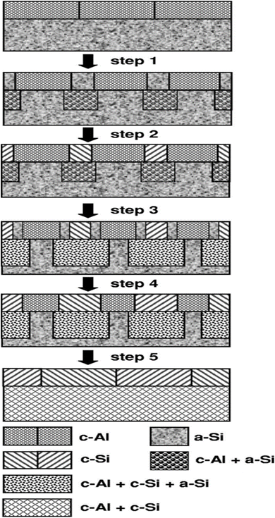 | ||
| Fig. 1 A schematic presentation of the mechanism of the Al induced layer exchange process. [Reproduced/adapted from Wang et al.,16 J. Appl. Phys., 2007, 102, 113523, with the permission from AIP Publishing.] | ||
Step-1: Diffusion of Si atoms along the Al GBs to form a-Si layers at the Al GBs. Step 2: Nucleation of Si crystallites after formation of 4 ML (1 ML = 0.22 nm) of a-Si layer at the Al GB. Step 3: Continuous diffusion of Si atoms along the new c-Al/c-Si interfaces. Step 4: Lateral growth of c-Si grains in Al sublayer after thickness of a-Si layer becomes 2 ML. Step 5: Formation of a continuous c-Si layer at the original location of Al layer via repetition of steps 3 and 4.
In all the above steps, it can also be observed that the Al atoms diffuse into the original location of a-Si sublayer due to the Si atoms diffusion into the original Al sublayer (i.e. along Al GBs and c-Al/c-Si interfaces). Finally, a mixture of c-Al and c-Si layer is developed at the original location of a-Si sublayer.16 This mechanism is known as layer exchange mechanism, as has been mentioned earlier.
5. Effects of growth parameters on the MIC growth kinetics and microsctructures
There are several parameters, which play very crucial roles in microstructural study and growth kinetics in MIC process. The effect of some of the important growth parameters such as the effect of thermal budget (temperature and time), interfacial oxide layer, different metal, thickness ratio of metal/semiconductor, and substrates has been discussed here.In layer exchange, nucleation and growth in MIC process, annealing temperature and time are very important parameters.3 Pihan et al.126 investigated the formation of Si grains in Al/Si bilayer system annealed at 450 °C from 40 minutes to 90 minutes on a flowable oxide (FOx)-coated alumina substrate. The crystallization time or the annealing time has an important role on the shape of Si grains; the Si grains were observed to grow uniformly in all the lateral directions until their coalescence, which finally results in the development of a continuous film. The nucleation and conversion time (i.e. time required to produce the initial nuclei and to make a continuous film) decrease with increasing Al-induced crystallization (AIC) annealing temperature.17 The time needed for completion of whole layer exchange is known as crystallization time, which depends strongly on the annealing temperature. The activation energy changes with the method of deposition and thickness of interfacial layer. The activation energy for crystallization fraction of 50% in the temperature range of 425–550 °C was found to be approximately 1.447 eV in Al/Si bilayer system.127,128 At temperatures more than 450 °C, the growing grains compete with each other, and the oversaturation between the grains decreases. At low annealing temperatures, however, there is no contest between growing grains and the orientations with high growth rate in parallel direction to the surface. The competition between rapid lateral growth and (100) vertical growth most probably leads to the formation of twins in the growing grain.124 When the annealing temperature decreases, a reduction in the nucleation rate results in the increase in the grain size. At lower temperatures, the effective diffusion distance is longer, which may lead to development of larger depletion areas around the growing grains, opposing further nucleation. Consequently, the grains grow to a larger size before impingement occurs. The overall crystallization process, therefore, takes more time at lower annealing temperatures.9
A thermodynamically stable metal oxide diffusion barrier such as aluminum oxide (AlOx) layer is necessary to control the rapid interlayer diffusion and to form a continuous p-Si film. This layer acts as a membrane sandwiched between metal and semiconductor layers, which control the diffusion process without participating in the layer exchange process. This interfacial layer does not change its position throughout the inter-diffusion process of metal and semiconductor atoms. Several researchers have studied the formation of AlOx and its effects on crystallization process in detail.129–131 They showed that when the sample is exposed to oxygen at low temperatures (≤100 °C), an amorphous oxide film of relatively uniform thickness is formed. However, at higher temperatures (≥200 °C), initially an amorphous oxide film is formed, which gradually transforms into crystalline γ-Al2O3. The thickness of the oxide layer is found to be in 2–4 nm range for a growth temperature more than 200 °C. Thickness of the oxide layer is a function of the interval of the air exposure: an exposure of one week, one day, and three minutes resulted in a thickness of 125 Å, 64 Å, and 50 Å, respectively. Thickness affects the duration of crystallization process: for one-week samples, the crystallization was found to be completed by annealing it at 500 °C.132 The continuous poly-Si film was obtained with the average grain size of 10 μm. The grain size was getting smaller by lowering the thickness of the aluminum oxide layer because of a rapid nucleation rate. The porous silicon is formed when the AlOx layer is not present. It may, therefore, be concluded that the oxidation thickness influences the nucleation process and its growth rate. Also it may be noted that this interfacial layer does not reduce the crystallization temperature and time significantly in MIC process as this layer acts as a traffic at the interface during diffusion of metal and semiconductor atoms.129–132
Some metals assist crystallization of a-semiconductors at low temperature, which are categorized in three groups: (a) post-transition metals (Al, In, Sn, Pb, Sb, and Bi) (b) transition metals (Ni, Pd, Pt, Cu, Ag, Au, and Zn) and (c) refractory metals (Mn, Co, Fe, Cr, V, Rh, Hf, Ti, Ir, Ru, Zr, Nb, Mo, W, Ta, and Re). The post-transition metals make simple eutectic binary systems with Si or Ge having very low MIC temperature, and do not form any compound phases in MIC. The transition metal crystallization is quite similar to post transition metal crystallization but in the latter case (e.g. especially in Ni, Pd, Pt and Cu) one or multiple compound phases with Si or Ge are formed in MIC. In case of refractory metals, the crystallization temperature of a-Si or a-Ge is high, but slightly lower than that of corresponding bulk crystallization temperatures. These metals form compounds before initiation of MIC. The crystallization of amorphous semiconductors have never been reported by using few metals such as Na, Mg, Y due to high reactivity of these metals in air. Therefore, it is an open problem for the scientific community to crystallize amorphous semiconductor using such metals. Gaudet et al.133 studied 20 transition metals (Ti, Zr, Hf, V, Nb, Ta, Cr, Mo, W, Mn, Re, Fe, Ru, Co, Rh, Ir, Ni, Pd, Pt, and Cu) and their effect on a-Ge crystallization. It was found that the first group of metals (Ti, Zr, Hf, V, Nb, and Ta) reacted with Ge only at temperatures well above 450 °C and another set (Cr, Mo, Mn, Re, Rh, Ru, and Ir) did not form low resistivity phases even when the system was annealed at up to 1000 °C. During the investigation, it was also found that Fe, Co, Ni, Pd, Pt, and Cu were the most interesting candidates for microelectronic applications as they reacted at relatively low temperatures (150–360 °C).
Nast et al.10 studied the effect of metal layer thickness on morphology of crystalline-semiconductors. It was shown that the porous structure in the AIC sample may be obtained if the Al layer was only twice the thickness of the a-Si layer. When the thickness of Si grains becomes equal to that of the Al film thickness, the growth of Si is confined to the plane bounded by the interface between the two layers and the substrate. This results in the lateral growth of the grains in the absence of sufficient amount of a-Si (as source). As the Si source is fully utilized before the nearer grains met, porosity develops in the layers.127 Therefore, the lack of Si prevents the development of a non-porous p-Si layer. If the a-Si layer is thicker than the Al layer, non-porous p-Si layer may be obtained on the substrate. Wang et al.134 discussed the effect of Al and a-Ge ratio in MIC process. Three sets of samples with configurations a-Ge (40 nm)/Al (80 nm), a-Ge (60 nm)/Al (60 nm), and a-Ge (60 nm)/Al (55 nm) were annealed to show that the average grain size of p-Ge are 20 μm, 50 μm, and 100 μm respectively. From above research contributions, it may be concluded that in order to form continuous p-Si and p-Ge films under steady temperature conditions, the a-Si and a-Ge layer must be at least as thick as the metal layer.
It has been observed that the rate of nucleation and the crystallographic quality of the p-Si and p-Ge seed layer obtained by MIC are controlled by the surface roughness of the substrate. Tuzun et al.135 studied the effect of FOx-coated alumina (surface roughness 160 nm) and SiN coated Corning glass (GC) substrates (surface roughness 8.2 nm) on crystallization of silicon. The distribution of the grain size in case of GC substrates was found to be more homogeneous, implying the constancy of the nucleation rate during the crystallization process.136,137 The average grain size of the AIC layer formed on GC substrate reached 25.2 μm, while it was close to 8 μm in case of alumina substrates. Oya et al.138 showed that a-Ge thin films were directly crystallized on flexible plastic substrates at 325 °C using Al-induced crystallization. The plastic substrate thickness strongly influenced the crystal quality of the resulting p-Ge layers. The reason behind this observation given was that when a thicker substrate is used, the stress on the a-Ge layer reduces during annealing, which increases the grain size and fraction of (111)-oriented grains within the Ge layer.
6. Ion mater interactions
Ion beam irradiation is a multipurpose tool to synthesize and modify the materials at nanometres scale. When an energetic ion passes through a material, it deposit huge amount of energy locally. The lighter ions with high energies (i.e. several hundreds of MeV per amu) lose their energy via Cherenkov, bremsstrahlung radiation, and nuclear reactions along with elastic collisions and ionizations.139 However, when heavy ions passes through the materials, they lose energy via inelastic collisions with target electrons (i.e. electronic energy loss: Se) and elastic collision with nucleus (i.e. nuclear energy loss: Sn).140,141 The rate of energy loss per differential path length (dE/dx), can be defined by the relation: , where ‘e’ and ‘n’ denote the electronic and nuclear collisions, respectively. The energy loss of ions can also be represented by the stopping cross section
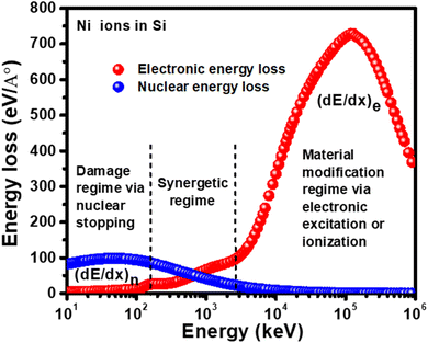
  , where N, Se and Sn, denote the atomic density of target materials, stopping cross section for electronic energy loss and stopping cross section for nuclear energy loss, respectively. The basic ion matter interaction process is coulombic. Nevertheless, pure coulomb potential predominates in electronic interaction case, whereas screened coulomb potential predominates in nuclear interaction case.142–144 Fig. 2 shows the variation of energy loss of Ni ions traversing through the Si target. The domination of nuclear energy loss and electronic energy loss are marked in the graph. The ions with low energy (i.e. few keV per amu) lose their energy dominantly by nuclear collision process resulting in atomic displacements. Swift heavy ions (i.e. when the ion velocity is greater than equals to the Bohr velocity of target electrons), however, lose their energy first by interacting with target electrons, ionizing them, and after slowing down they interact with screened target nuclei producing recoils/direct displacements. The electronic energy loss is dominated up to a certain depth and nuclear energy loss is overriding effect at the end of the range of ions. The maximum of electronic energy loss at certain depth is known as Bragg's peak.142
6.1. Range of the ions in materials
The total distance travelled by the ion inside the material is known as ion range (R), defined by the relation: . Here E0 is incident ion energy and [dE/dx]total is the sum of total electronic and nuclear stopping powers of the material. The projected range
  is defined as the projection of range along the axis of incidence ion. The statistical fluctuation in the projected range along the axis of incidence ion is called ‘projected range straggle σp or longitudinal straggling’ and the fluctuations along perpendicular axis is known as ‘lateral straggle σ⊥ or transversal straggling’.142
6.2. Nuclear energy loss in materials
In nuclear collisions, a large amount of discrete energy is transferred to the target materials resulting in significant angular deflection of the ions from their trajectory. The deposited energy through nuclear collisions produces lattice disorder via atomic displacements. Sometimes, these displaced atoms have sufficient energy to cause secondary displacements of the atoms, which form a tree of disorder along the ion path, known as collision cascade. Generally, the yield of disorder/defect formation depends on ion/target atomic mass ratio, and numbers of ions falling per unit area on target material known as ion fluence or ion dose. The disordered zones produced by different ions remain well separated from each other at low fluences. At the high fluence, disordered zones start to overlap and leads to the complete/partial amorphization of the material. The nuclear stopping process may be understood in terms of a binary classical elastic collision event between the incoming ions and the target atom.142–1446.3. Electronic energy loss in materials
In electronic energy loss process, the ion loses its energy through inelastic scattering by target electrons. This scattering leads to the electronic excitation and/or ionization of the target atoms and excited electrons transfer their energy to lattice. The electronic energy loss process mainly depends on the charge of the ion and target atoms and the relative velocity. Therefore, the electronic energy loss regime may be divided in two parts:145 in the first part, the ion velocity isv < v0Z2/31 and in the second part the ion velocity is v ≥ v0Z2/31 (i.e. for fast collision case), where v0 is Bohr velocity and Z1 is the atomic number of the ion. For the high energy regime, the velocity of the incident ion is greater than the mean orbital velocity of the target electrons (i.e. v ≥ v0Z2/31). In this case, the ions are fully stripped and behaves like a positive point charge. According to Bethe and Bloch, if the electronic energy loss is in the non-relativistic limits, the stopping cross-section decreases with increasing ion velocity.145,1466.4. Coulomb explosion model
The Coulomb explosion model was proposed to explain the formation of ion track in insulators due to the ionization along the ion path.147,148 When ion passes through a material, the energy of ions is transferred to the electrons of target materials via inelastic collisions, resulting in the ejection of electrons from a cylindrical volume (i.e. track core in target material), as shown in Fig. 3(a and b). The ejected electrons are called delta electrons. The ejection process lasts only for 10−17 second after the passing of ions. These delta electrons may further generate secondary electrons by excitation and ionization in track halo region. Then, the ions in the core move away from the core within 10−13 to 10−15 second due to the repulsive Coulomb force. This phenomenon is known as Coulomb explosion, which leads to a localized destruction in lattice structure via the production of vacancies and interstitials. However, the delta electrons finally move back towards the core after losing their energy via inelastic collisions. Generally, the track core diameter is only a few nanometres (nm), while the halo diameter is in the range of 100 nm to 1000 nm. The track core is important for modification of Alkali halides, whereas track halo has more importance in modification of semiconductor, polymers, and biological objects.142,149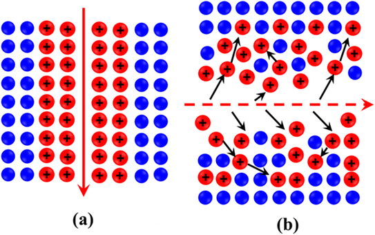 | ||
| Fig. 3 Schematic of (a) cylindrical positive ion core after passage of ions through mater and (b) generation of delta electrons. | ||
6.5. Thermal spike model
In thermal spike model, the free electrons generated due to excitation and/or ionization are trapped within a narrow cylindrical zone around the ion path known as the ion track. The electron confinement depends on electron diffusion length, which modifies the electron–phonon coupling (g). The coupling term ‘g’ governs the efficiency by which the energy is deposited in the electronic subsystem and subsequently transferred to the lattice subsystem per unit volume. The coupling term also decides the rate of increase of the lattice temperature. The two-temperature model can be used to describe the rise in temperature of the lattice, and is given as a set of two coupled heat diffusion equations:150,151Here, r is the radial distance from the path of ion or track radius; Te, Ta, Ce, Ca, Ke, Ka represent temperature, specific heat and thermal conductivity for the electronic and atomic subsystems, respectively. Numerical solution of these coupled partial differential equations give time evolution of the temperature along the ion track. If the local temperature inside the cylindrical zone is found to be above the critical temperature of phase transformation (i.e. evaporation, crystallization etc.), then material will transform accordingly. After completion of Coulomb explosion process (10−15 to 10−13 s), the thermal spike takes place in the interval 10−14 to 10−12 s. The time span of thermal spike is very short, therefore the materials modification due to ion irradiation is a very fast process. This model has been widely used to describe the track formation, defect annealing, recrystallization in semiconductors and metal modifications etc.150–157
7. Ion beam induced crystallization of amorphous semiconductors thin films
As discussed above that the as-grown crystalline-Si (c-Si) and crystalline-Ge (c-Ge) films are found to have higher or lower density of electrically active microstructural defects (depends on annealing temperature). These defects move forward to the epitaxial layer, resulting in the lowering of electronic quality of the absorber layer. On the other hand, the high-temperature-deposited epitaxial films have lower defect density than the low-temperature-deposited films. The solar cell, which uses the MIC seed layer, has been observed to show a photovoltaic conversion efficiency of 8% due to the bad grains quality and diffusion of impurities atoms from the substrates in high-temperature annealing. In spite of the above, the use of p-Si and p-Ge seed layers formed by MIC in thin-film solar cells has been considerable. However, basic physical characteristics of MIC grown polycrystalline semiconductors films still required to be improved significantly in order to use it as an effective solar cell material. The previous explorations showed that p-Si and p-Ge produced by MIC process are the potential candidate for photovoltaic applications. However, further advancement in this process is still needed for synthesizing highly efficient solar cells and high quality flat panel displays. There are several limitations of MIC process. The most obvious limitation is that the crystallization temperature in MIC is high. In addition, since the whole substrate is heated almost uniformly, it is not possible to crystallize the amorphous material in spatially selective way. In conventional MIC (using thermal annealing), it is not possible to control the depth of crystallization. In this respect, swift heavy ion irradiation offers the possibilities for metal-induced crystallization of a-semiconductors in a controlled way with great precision (through ion dose), spatial selectivity (either by focusing or high energies) and depth (through energy). Swift heavy ion (SHI) irradiation is an innovative, valuable and very powerful tool in investigating various fields of modern technology, e.g. synthesis of nanoclusters in thin films, phase transformations, surface and interface modification etc.157 Swift heavy ion, when passing through a material creates a high yield of electronic excitations over a small cylindrical zone of a few nanometers in diameter around its path, termed as ion track. Presently, two theoretical models, Coulomb explosion model and thermal spike model157 have been proposed to explain the local excitation of the lattice by energy transfer from the electronic system.7.1. Metal induced crystallization of a-Si under ion beam irradiation
Recently, Maity et al.,157–159 used thermal annealing and ion irradiation to investigate the crystallization of a-Si in Al/a-Si bilayer thin films. The effect of all parameters affecting the crystallization like thickness ratio of Al and a-Si layers, annealing temperature, ion fluence, and temperature during ion irradiation was explored in detail. Two sets of samples were prepared on oxidized Si-substrates by thermal evaporation (Al deposition) and e-beam techniques (a-Si deposition): set-A samples with thickness ratio 1![[thin space (1/6-em)]](https://www.rsc.org/images/entities/char_2009.gif) :
:![[thin space (1/6-em)]](https://www.rsc.org/images/entities/char_2009.gif) 1 (50 nm Al/50 nm a-Si) and set-B samples with thickness ratio 1
1 (50 nm Al/50 nm a-Si) and set-B samples with thickness ratio 1![[thin space (1/6-em)]](https://www.rsc.org/images/entities/char_2009.gif) :
:![[thin space (1/6-em)]](https://www.rsc.org/images/entities/char_2009.gif) 3 (50 nm Al/150 nm a-Si). Both the sets of samples were irradiated by 100 MeV Ni7+ ions with fluences of 1 × 10¹² ions per cm2, 5 × 10¹² ions per cm2, 1 × 10¹³ ions per cm2, and 5 × 10¹³ ions per cm2 at 100 °C and 200 °C. In Fig. 4(a)–(c), Raman spectra of pristine and irradiated set-A and set-B samples (at 100 °C with different fluence) have been displayed. In both the pristine sample sets, a broad and weak hump of a-Si at lower wavenumber (∼480 cm−1) is observed, which confirms the amorphous nature of Si. In the irradiated sample sets, a Raman peak at 520 cm−1 is observed, which corresponds to the transverse optical (TO) phonon mode of c-Si. The intensity of the peak is observed to decrease with increasing ion fluence, which confirms a reduction in the crystallinity due to irradiation-induced amorphization. Similar results were also observed for the samples irradiated at 200 °C. Fig. 4(b)–(d) show the grazing incidence X-ray diffraction (GIXRD) pattern of pristine and samples of set-A and set-B, respectively, irradiated at 100 °C temperature with different fluences. In the pristine samples of both the sets, only a single diffraction peak at 2θ of 39.94° corresponding to Al (111) lattice plane is observed. No other peak corresponding to c-Si is observed in the pristine samples. However, after ion irradiation at 100 °C, another peak is observed at 2θ of 28° (in addition to the Al (111) peak) assigned to the diffraction from Si (111) lattice plane. The intensity of the peak is observed to be higher at the lowest fluence. This indicates that the crystallization of Si decreases with increasing ion fluence. Similar results were also observed for the samples irradiated at 200 °C. XTEM measurements of pristine and irradiated samples (at a fluence of 5 × 10¹² ions per cm2 and temperature 100 °C) further confirms the crystallization process in the irradiated samples, as shown in Fig. 5. From the XTEM micrographs of both the sets of pristine samples, no sign of interface diffusion was noticed (see Fig. 5(a)–(d)). However, in case of irradiated samples, interface diffusion (i.e. due to atomic transport across the interface) was observed, which has been shown in Fig. 5(b)–(e). High-resolution TEM (HRTEM) images of the interface clearly shows the crystallization of a-Si for both the sets of samples (see Fig. 5(c)–(f)).157–159
3 (50 nm Al/150 nm a-Si). Both the sets of samples were irradiated by 100 MeV Ni7+ ions with fluences of 1 × 10¹² ions per cm2, 5 × 10¹² ions per cm2, 1 × 10¹³ ions per cm2, and 5 × 10¹³ ions per cm2 at 100 °C and 200 °C. In Fig. 4(a)–(c), Raman spectra of pristine and irradiated set-A and set-B samples (at 100 °C with different fluence) have been displayed. In both the pristine sample sets, a broad and weak hump of a-Si at lower wavenumber (∼480 cm−1) is observed, which confirms the amorphous nature of Si. In the irradiated sample sets, a Raman peak at 520 cm−1 is observed, which corresponds to the transverse optical (TO) phonon mode of c-Si. The intensity of the peak is observed to decrease with increasing ion fluence, which confirms a reduction in the crystallinity due to irradiation-induced amorphization. Similar results were also observed for the samples irradiated at 200 °C. Fig. 4(b)–(d) show the grazing incidence X-ray diffraction (GIXRD) pattern of pristine and samples of set-A and set-B, respectively, irradiated at 100 °C temperature with different fluences. In the pristine samples of both the sets, only a single diffraction peak at 2θ of 39.94° corresponding to Al (111) lattice plane is observed. No other peak corresponding to c-Si is observed in the pristine samples. However, after ion irradiation at 100 °C, another peak is observed at 2θ of 28° (in addition to the Al (111) peak) assigned to the diffraction from Si (111) lattice plane. The intensity of the peak is observed to be higher at the lowest fluence. This indicates that the crystallization of Si decreases with increasing ion fluence. Similar results were also observed for the samples irradiated at 200 °C. XTEM measurements of pristine and irradiated samples (at a fluence of 5 × 10¹² ions per cm2 and temperature 100 °C) further confirms the crystallization process in the irradiated samples, as shown in Fig. 5. From the XTEM micrographs of both the sets of pristine samples, no sign of interface diffusion was noticed (see Fig. 5(a)–(d)). However, in case of irradiated samples, interface diffusion (i.e. due to atomic transport across the interface) was observed, which has been shown in Fig. 5(b)–(e). High-resolution TEM (HRTEM) images of the interface clearly shows the crystallization of a-Si for both the sets of samples (see Fig. 5(c)–(f)).157–159
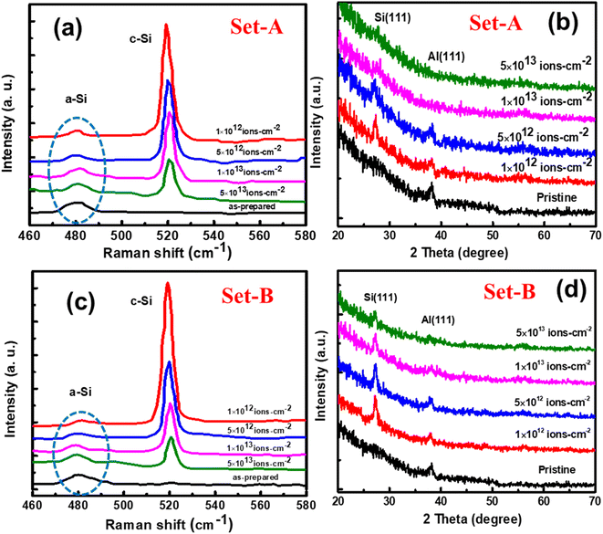 | ||
| Fig. 4 (a) Raman spectra (b) XRD pattern of set-A irradiated by 100 MeV Ni ions at 100 °C with different fluence of 1 × 10¹² ions per cm2, 5 × 10¹² ions per cm2, 1 × 10¹³ ions per cm2, and 5 × 10¹³ ions per cm2. And (c) Raman spectra (d) XRD of set-B irradiated at 100 °C with different fluences at 100 °C with different fluence of 1 × 10¹² ions per cm2, 5 × 10¹² ions per cm2, 1 × 10¹³ ions per cm2, and 5 × 10¹³ ions per cm2. [Reproduced/adapted from Maity et al.,157 RSC Adv., 2020, 10, 4414, with permission from The Royal Society of Chemistry.] | ||
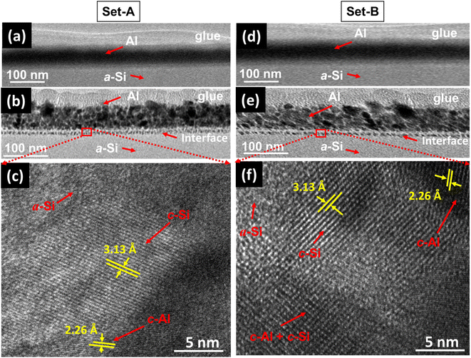 | ||
| Fig. 5 XTEM and high resolution TEM (HRTEM) micrograph of both bilayer system (set-A & set-B) with pristine and irradiated with 5 × 10¹² ions per cm2 at temperature of 100 °C. For set-A sample (a) XTEM image of pristine sample (b) XTEM image of irradiated sample (c) HRTEM image of the interface for irradiated sample. For set-B sample (d) XTEM image of pristine (e) XTEM image of irradiated sample (f) HRTEM image of the interface for irradiated sample. [Reproduced/adapted from Maity et al.,157 RSC Adv., 2020, 10, 4414, with permission from The Royal Society of Chemistry.] | ||
The effect of irradiation temperature (i.e. 100 °C and 200 °C) on crystallization has been understood by Raman spectra of set-B samples as has been displayed in in Fig. 6(a–d). It is observed that the Raman peak intensity corresponding to c-Si at all fluences is higher at 100 °C than that of 200 °C. This represents that the crystallinity in the samples irradiated at 100 °C is better as compared to the sample irradiated at 200 °C. Similar observation has also been recorded for set-A samples also.157–159
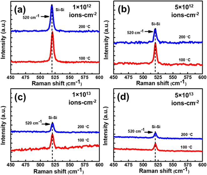 | ||
| Fig. 6 Raman spectra of set-B sample irradiated at 100 °C and 200 °C with the different fluences of (a) 1 × 10¹² ions per cm2, (b) 5 × 10¹² ions per cm2, (c) 1 × 10¹³ ions per cm2, and (d) 5 × 10¹³ ions per cm2. (All figures are plotted in same y-scale range for comparison). [Reproduced/adapted from Maity et al.,157 RSC Adv., 2020, 10, 4414, with permission from The Royal Society of Chemistry.] | ||
The effect of thickness ratio on crystallization in irradiated samples has also been studied by Raman and GIXRD measurements. Raman peak intensities for irradiated samples at 100 °C having thickness ratio 1![[thin space (1/6-em)]](https://www.rsc.org/images/entities/char_2009.gif) :
:![[thin space (1/6-em)]](https://www.rsc.org/images/entities/char_2009.gif) 1 (Fig. 7(a–d)) are observed to be lower than the samples with thickness ratio 1
1 (Fig. 7(a–d)) are observed to be lower than the samples with thickness ratio 1![[thin space (1/6-em)]](https://www.rsc.org/images/entities/char_2009.gif) :
:![[thin space (1/6-em)]](https://www.rsc.org/images/entities/char_2009.gif) 3, indicating higher crystallization in samples having thickness ratio 1
3, indicating higher crystallization in samples having thickness ratio 1![[thin space (1/6-em)]](https://www.rsc.org/images/entities/char_2009.gif) :
:![[thin space (1/6-em)]](https://www.rsc.org/images/entities/char_2009.gif) 3. Similar observations have also been recorded with the GIXRD pattern (Fig. 8(a–d)) of the irradiated samples: irradiated samples with thickness ratio 1
3. Similar observations have also been recorded with the GIXRD pattern (Fig. 8(a–d)) of the irradiated samples: irradiated samples with thickness ratio 1![[thin space (1/6-em)]](https://www.rsc.org/images/entities/char_2009.gif) :
:![[thin space (1/6-em)]](https://www.rsc.org/images/entities/char_2009.gif) 3 have high peak intensities as compared to the samples with thickness ratio 1
3 have high peak intensities as compared to the samples with thickness ratio 1![[thin space (1/6-em)]](https://www.rsc.org/images/entities/char_2009.gif) :
:![[thin space (1/6-em)]](https://www.rsc.org/images/entities/char_2009.gif) 1. These observations indicate the preferential growth of c-Si along (111) direction at all fluences in both the sets of samples. Similar results have also been observed for both sets of samples irradiated at 200 °C.157–159
1. These observations indicate the preferential growth of c-Si along (111) direction at all fluences in both the sets of samples. Similar results have also been observed for both sets of samples irradiated at 200 °C.157–159
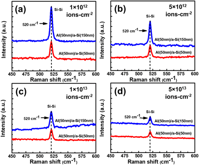 | ||
| Fig. 7 Raman spectra of set-A and set-B samples irradiated at 100 °C with different fluences of (a) 1 × 10¹² ions per cm2, (b) 5 × 10¹² ions per cm2, (c) 1 × 10¹³ ions per cm2, and (d) 5 × 10¹³ ions per cm2. (All figures are plotted in same y-scale range for comparison). [Reproduced/adapted from Maity et al.,157 RSC Adv., 2020, 10, 4414, with permission from The Royal Society of Chemistry.] | ||
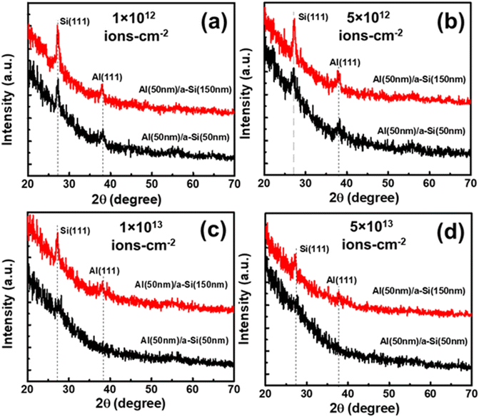 | ||
| Fig. 8 GIXRD pattern of set-A and set-B samples irradiated at 100 °C with different fluences of (a) 1 × 10¹² ions per cm2, (b) 5 × 10¹² ions per cm2, (c) 1 × 10¹³ ions per cm2, and (d) 5 × 10¹³ ions per cm2. (All figures are plotted in same y-scale range for comparison). [Reproduced/adapted from Maity et al.,157 RSC Adv., 2020, 10, 4, 414, with permission from The Royal Society of Chemistry.] | ||
The results conclude that the crystallization of Si happens at surprisingly low temperature of 100 °C under ion irradiation for both the set of samples at all ion fluences. The samples irradiated at 100 °C were found to show better crystallization than the samples irradiated at 200 °C at all ion fluences. At a fluence of 1 × 10¹² ions per cm2, maximum crystallization has been observed for both the set of samples. Crystallization was observed to decrease with increasing ion fluence at both the temperatures of 100 °C & 200 °C. The crystallization of set-B samples was found to be better as compared to set-A samples at all the irradiation temperatures and fluences.
The possible mechanisms behind crystallization in all the cases have been discussed in detail with the help of various theoretical formulations.157–159 In the current investigation, irradiation is carried out at higher temperature (100 °C and 200 °C). Irradiation produces non-equilibrium concentration of defects as well as local lattice heating, which may be estimated via thermal spike model (see Fig. 9(a–f)). Therefore, due to the thermal spike temperature, irradiation temperature and availability of non-equilibrium concentration of defects, the kinetics of defects is enhanced many folds. Additionally, since Si interstitials are faster diffusing species than Al interstitials,160 Si interstitials may reach the interface faster and recombine with the vacant sites available there to become the lattice atoms, which might be the reason behind the crystallization of Si near the interface region. The crystallinity of Si is found better in set-B samples than in set-A samples, which might have been due to availability of more Si interstitials for crystallization in set-B (thickness of Si film is 150 nm) than set-A (thickness if Si film is 50 nm) samples. High-energy irradiation in set-B samples leads to more atomic displacements and hence more Si interstitials than in set-A samples. In addition to the defect-mediated diffusion, the mechanical and thermal stresses developed during irradiation may also enhance the kinetics of the defects. It is also observed that the crystallinity in Si is better when the samples are irradiated at 100 °C than at 200 °C. The lattice temperature of the sample (consisting of c-Al and a-Si) is found to be higher when it is irradiated at 200 °C than that of 100 °C (see in Fig. 9(e and f)). At high lattice temperature (irradiated at 200 °C), back-diffusion of Si atoms to the matrix from the c-Si phase via vacancy mechanism might be the reason behind lower crystallinity at 200 °C.157–159
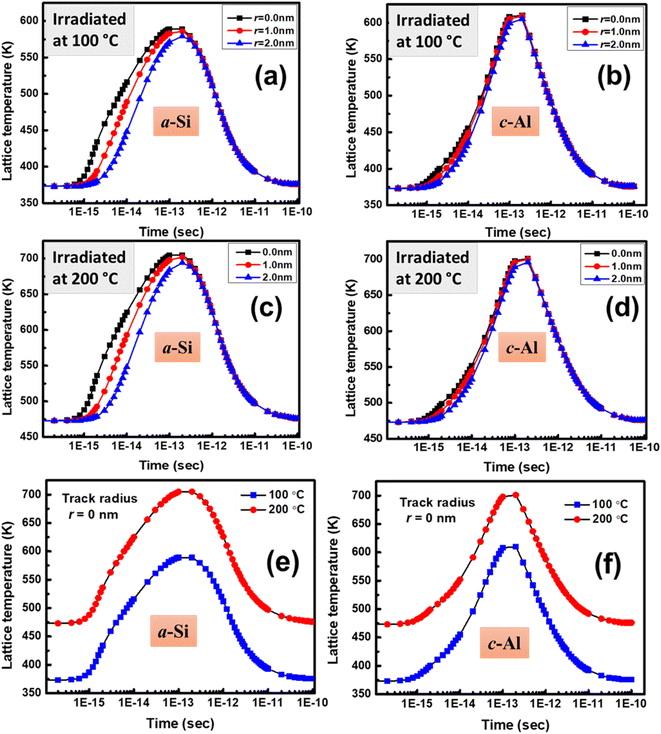 | ||
| Fig. 9 Thermal spike calculation for the estimation of lattice temperature in (a) a-Si and (b) c-Al due to 100 MeV Ni ion irradiation and for the track radii r = 0, 1, 2 nm when samples irradiated at 100 °C. Lattice temperature in (c) a-Si and (d) c-Al due to 100 MeV Ni ion irradiation and for the track radii r = 0, 1, 2 nm when samples irradiated at 200 °C. (e) Lattice temperature of a-Si at 100 °C and 200 °C. (f) Lattice temperature of c-Al at 100 °C and 200 °C. [Reproduced/adapted from Maity et al.,157 RSC Adv., 2020, 10, 4414, with permission from The Royal Society of Chemistry.] | ||
Very recently, Maity et al.161 have successfully developed p-Si thin films at room temperature (RT) using 500 keV Xe+ ion irradiation. In order to do this, c-Al (50 nm/a-Si (150 nm)) bilayer thin films have been used for ion irradiation experiments. The structural studies showed that the crystallization of Si started at a threshold fluence of 3 × 10¹⁵ ions per cm2 and crystallinity was found to increase with increasing ion fluence. Fig. 10(a and b) confirmed the results. The results were explained in terms of displacement spike and thermal spike due to the interaction of energetic ions with target atoms.
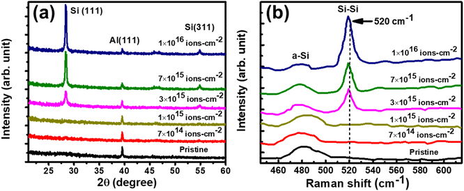 | ||
| Fig. 10 (a) XRD pattern (b) Raman spectra of pristine sample and the samples irradiated with different ion fluence of 7 × 10¹⁴ ions per cm2, 1 × 10¹⁵ ions per cm2, 3 × 10¹⁵ ions per cm2, 7 × 10¹⁵, and 1 × 10¹⁶ ions per cm2. [Reproduced/adapted from Maity et al.,161 J. Appl. Phys., 2022, 132, 095303, with the permission from AIP Publishing.] | ||
7.2. Metal induced crystallization of a-Ge under ion beam irradiation
Maity et al. have reported Au induced crystallization of a-Ge via ion irradiation followed by thermal annealing.162 The a-Ge (50 nm)/Au (50 nm) bilayer thin films (i.e. a-Ge/Au) on quartz substrate were deposited by means of e-beam (a-Ge deposition) and thermal (Au deposition) evaporation techniques in a high vacuum (∼6 × 10⁻⁷ mbar) chamber without interrupting the vacuum. The as-prepared samples were irradiated with 100 MeV Ni7+ ions at different fluences of 1 × 10¹² ions per cm2, 5 × 10¹² ions per cm2, 1 × 10¹³ ions per cm2 and 5 × 10¹³ ions per cm2. The ion irradiation does not show any crystallization of Ge; instead, an increase in ion fluence decreases the Au crystallite size. The smaller crystallite size of Au, leads to higher grain boundary (GB) density (i.e. high defect sink density) at higher ion fluence. Under ion irradiation, inter-diffusion of Ge and Au atoms across the interface region has been observed. The results are confirmed by XRD, transport of ions in matter (TRIM) simulation and Rutherford back scattering spectroscopic (RBS) data, as shown in Fig. 11. The higher GB density has been observed to result in better crystallization of a-Ge, as the free Ge atoms get more space to diffuse into the GB of Au during thermal annealing. In order to crystallize the Ge, the ion irradiated samples were post-annealed at a fixed temperature of 300 °C for 4 h in N2 atmosphere. The crystallization was studied by XRD and Raman measurements. The XRD and Raman data are shown in Fig. 12. The crystallization of Ge is found better for the samples irradiated at higher fluence; Ge is found to be poly-crystalline in nature for all fluences. This may be due to the higher grain boundary density (i.e. for higher ion fluence) in Au after irradiation, which might have been helpful in accumulating free Ge atoms near the grain boundaries. The detailed mechanism has been discussed through MIC process and band theory.162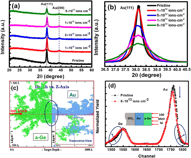 | ||
| Fig. 11 (a) XRD pattern of a-Ge/Au pristine and ion irradiated thin films at different fluence of 1 × 10¹² ions per cm2, 5 × 10¹² ions per cm2, 1 × 10¹³ ions per cm2, and 5 × 10¹³ ions per cm2 (b) variation of FWHM of Au (111) diffraction peak with ion fluences. (c) TRIM simulation of (depth vs. Z-axis) a-Ge (i.e. layer 1 colored by green) and Au (i.e. layer 2 colored by blue) at the interface (mixing region shown by ring). The inset shows the transvers view of the TRIM simulation (d) RBS spectra of pristine and ion irradiated a-Ge/Au thin film at fluence of 5 × 10¹³ ions per cm2. [Reproduced/adapted from Maity et al.,162 CrystEngComm, 2020, 22, 666, with permission from The Royal Society of Chemistry.] | ||
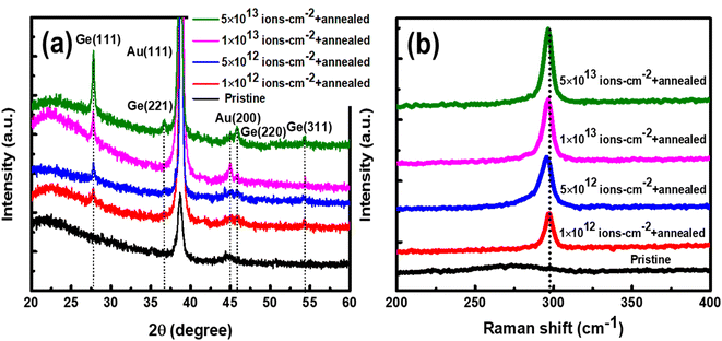 | ||
| Fig. 12 (a) XRD pattern and (b) Raman spectra of pristine sample and samples post-annealed (after ion irradiation at different fluences) at 300 °C. The XRD and Raman results clearly show the crystallization of Ge due to thermal annealing treatment after ion irradiation. [Reproduced/adapted from Maity et al.,162 CrystEngComm, 2020, 22, 666, with permission from The Royal Society of Chemistry.] | ||
However, from the above discussion in Sections 7.1 and 7.2 it is observed that a-Si film in contact with Al is crystallized at surprisingly low temperature of 100 °C under 100 MeV Ni ions irradiation. Further, a-Si thin films is crystallized at room temperature (RT) using 500 keV Xe+ ion irradiation. But in a-Ge/Au system, a-Ge is crystallized via ion irradiation followed by thermal annealing at 300 °C. In several studies, Al-induced crystallization (AIC) of a-Si and a-Ge via thermal annealing is observed to take place at comparatively lower temperature than Au-induced crystallization (GIC).8–29 Under ion beam irradiation, however, it is still unclear why a-Ge is not crystallized at low temperatures. Therefore, rigorous investigations are needed to understand metal-induced crystallization (using Al, Au, Cu etc.) of a-Ge via ion beam irradiations.
7.3. Application of metal induced crystallized Si and Ge under ion irradiation
Recently Maity et al.,159 explored the surface properties of c-Si and c-Ge developed by ion beam irradiation for solar cell application. As discussed above, the best crystallization of Si was achieved at an ion fluence of 1 × 10¹² ions per cm2; crystallinity was found to decrease with increasing ion fluence. The contact angle (CA) of the absorber surfaces (i.e. Al incorporated c-Si and/or homogeneous c-Si layer, obtained after selective chemical etching of top unreacted Al) was found to decrease with increasing ion fluence and the surfaces were hydrophobic in nature. The hydrophobicity was found to decrease with increasing ion fluence. The dependence of wettability and optical properties on various statistical, fractal, and multifractal parameters was critically and carefully investigated via atomic force microscopy (AFM) images along with system energy/unit cell and the related Laplace pressure calculations. Further, the calculation of multiple scattering cross-sections of light together with optical reflectivity analyses suggest that the absorber surface of the best crystalline film has the lowest optical reflectance. These results were confirmed by the analysing different data, as shown in Fig. 13–15. Therefore, the results suggest that such surfaces with low optical reflectance and hydrophobic nature may be used as a photon absorber layers for advanced solar cell devices besides its self-cleaning nature.159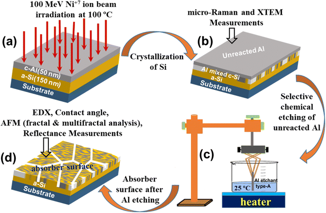 | ||
| Fig. 13 The schematic of experimental details where (a) ion beam irradiation of bilayer sample (b) sample after irradiation (c) etching of unreacted Al from the top layer of sample (d) absorber surface after Al etching. [Reproduced/adapted from Maity et al.,159 J. Appl. Phys., 2021, 129, 045301, with the permission from AIP Publishing.] | ||
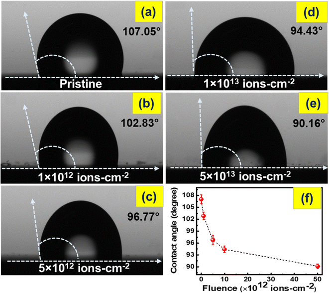 | ||
| Fig. 14 Contact angles (CA) of (a) pristine film, and absorber films developed at different fluences of (b) 1 × 10¹² ions per cm2, (c) 5 × 10¹² ions per cm2, (d) 1 × 10¹³ ions per cm2, and (e) 5 × 10¹³ ions per cm2. (f) Variation of CA with ion fluence. [Reproduced/adapted from Maity et al.,159 J. Appl. Phys., 2021, 129, 045301, with the permission from AIP Publishing.] | ||
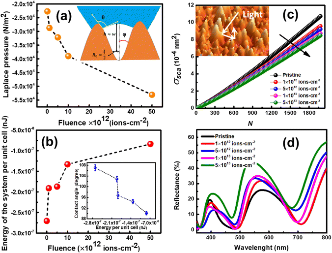 | ||
| Fig. 15 (a) Variation of laplace pressure of the absorber film surfaces with ion fluence. The inset figure is the schematic diagram of interaction between water droplet and conical surface array. (b) Variation of system energy/unit cell (Ec) with the ion fluence. Insert figure shows the variation of contact angle with the system energy/unit cell (Ec). (c) Scattering cross section (σsca) as a function of number of constituent particle (N) on absorber film surface. Inset figure demonstrate the schematic of multiple scattering of light. (d) Reflectance spectra of pristine film, and absorber films developed at different fluences. [Reproduced/adapted from Maity et al.,159 J. Appl. Phys., 2021, 129, 045301, with the permission from AIP Publishing.] | ||
Maity et al. in their other work,162 obtained polycrystalline Ge films by ion irradiation followed by thermal annealing. The energy band gap of polycrystalline Ge was determined by reflectance and transmittance spectra, and was observed to be low (∼0.64 eV) at higher fluence. The field emission scanning electron microscopy (FESEM) and AFM analyses showed that the surface microstructure changes for post-annealed samples irradiated at different fluences. The importance of fractal like surface microstructure in multiple scattering of light on the film surface has been discussed in detail. These results were confirmed by the analysis of different characterization data, as shown in Fig. 16 and 17. Poly-Ge is a promising material for solar cell applications due to lower value of resistivity, sheet resistance and good optical properties.162
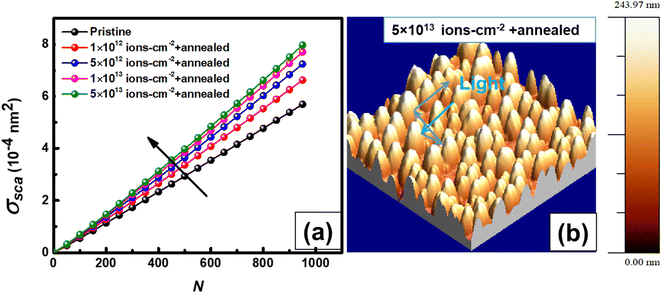 | ||
| Fig. 16 (a) Scattering cross section (σsca) as a function of number of constituent grain (N) on film surface (b) three-dimensional AFM image of post-annealed (at 300 °C) sample irradiated at fluence of 5 × 10¹³ ions per cm2 to demonstrate the schematic of multiple scattering of light. [Reproduced/adapted from Maity et al.,162 CrystEngComm., 2020, 22, 666, with permission from The Royal Society of Chemistry.] | ||
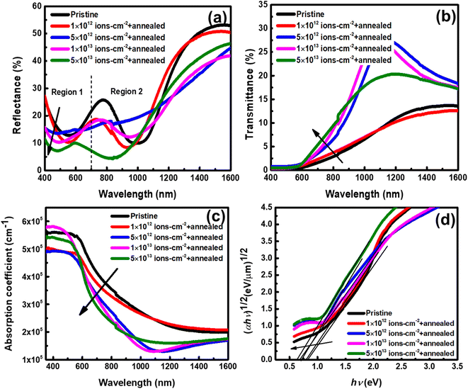 | ||
| Fig. 17 (a) Reflectance, and (b) transmittance spectra of pristine sample and post-annealed (at 300 °C) samples after ion irradiation at different fluences. (c) Absorption coefficient and (d) plot of (αhν)1/2 vs. photon energy (hν) for pristine sample and post annealed (at 300 °C) samples after ion irradiation at different fluences. [Reproduced/adapted from Maity et al.,162 CrystEngComm., 2020, 22, 666, with permission from The Royal Society of Chemistry.] | ||
8. Suggestions for future researches, challenges, and applications
According to above discussed results, the MIC via ion beam irradiation needs to be explored in more detail to find out the critical parameters of crystallization such as thin films parameters (i.e. film thickness, ratio of metal to semiconductor film thickness, and deposition rate etc.), ion beam parameters (i.e. ion mass, ion energy, and ion fluence), and elevated temperature (i.e. less than the reported one). In addition, there are challenges in synthesizing poly-crystalline semiconductor thin films with metal contact via ion beam irradiation at very low temperature (i.e. room temperature). One can also study the effects of growth parameters such as different metal layer, thickness ratio of metal/semiconductor, interfacial oxide layer, stacking change of metal and semiconductors layer etc on the crystallization process. Researchers can also explore MIC of compound semiconductors (i.e. SiGe, TiO2, InP, CdS etc.) and other elemental semiconductor (i.e. C) thin films in addition to Si and Ge via ion beam irradiation as a new tool. These aspects of MIC may be helpful for further development of compound and elemental semiconductors based high efficiency solar cells, which could address the green energy demand and supply chain issues, and develop high quality flat panel displays.9. Conclusion
This article presents a comprehensive account of all the synthesis methods that have been employed so far to prepare p-Si and p-Ge films with the help of metals. In addition, an outlook on the state of the art of p-Si and p-Ge devices along with the analysis of different factors that limit the efficiency of a solar cell and quality of the flat panel displays has also been presented. Finally, few suggestions have been included for development of c-Si, c-Ge, compound semiconductors (i.e. SiGe, TiO2, InP, CdS etc.) and other elemental semiconductor (i.e. C) thin films for solar cells, flat panel displays and other applications at very low temperature via ion beam irradiation as a new tool. Therefore, a systematic research methodology is necessary to address all the complexities/challenges in ensuring better crystallization of amorphous materials. We believe that this review article will inspire the readers to perform a thorough investigation on various aspects of MIC for further development of materials for efficient green energy harvesting via solar cells, which could be instrumental in addressing the green energy demand and supply chain. The MIC scheme may also help in developing materials for high quality flat panel displays.Data availability
The data that support the findings of this study are openly available in following details: (1). AIP Publishing, at https://doi.org/10.1063/1.2822275, ref. 16; (2). Taylor & Francis Group, at https://doi.org/10.1201/b18032, ref. 120; (3). RSC Publishing, at https://doi.org/10.1039/C9RA08836A, ref. 157; (4). AIP Publishing, at https://doi.org/10.1063/5.0023474, ref. 159; (5). RSC Publishing, at https://doi.org/10.1039/C9CE01584A, ref. 162. (6). AIP Publishing, at https://doi.org/10.1063/5.0099262, ref. 161Conflicts of interest
The authors declare that they have no conflict of interest.Acknowledgements
This work is financially supported by UGC, New Delhi in the form of User Funded Research project UFR No. -58308 (through IUAC, New Delhi). TM is thankful to IUAC, New Delhi for providing finacial assistant through UFR No. 69306 research grant. SPP is thankful to the UGC and DST, Government of India, New Delhi for supporting the Department of Pure and Applied Physics through UGC-SAP, DRS-1 and FIST Level-1 program, respectively.References
- I. Gordon, L. Carnel, D. Van Gestel, G. Beaucarne and J. Poortmans, Prog. Photovolt: Res. Appl., 2007, 15, 575 CrossRef CAS.
- A. Okada, K. Toko, K. O. Hara, N. Usami and T. Suemasu, J. Cryst. Growth, 2012, 356, 65–69 CrossRef CAS.
- O. Tuzun, Y. Qiu, A. Slaoui, I. Gordon, C. Maurice, S. Venkatachalam, S. Chatterjee, G. Beaucarne and J. Poortmans, Sol. Energy Mater. Sol. Cells, 2010, 94, 1869–1874 CrossRef.
- K. R. Catchpole, M. J. McCann, K. J. Weber and A. W. Blakers, Sol. Energy Mater. Sol. Cells, 2001, 68, 173–215 CrossRef CAS.
- R. B. Bergmann, G. Oswald, M. Albrecht and V. Gross, Sol. Energy Mater. Sol. Cells, 2001, 68, 173–215 CrossRef.
- T. Matsuyama, N. Terada, T. Baba, T. Sawada, S. Tsuge, K. Wakisaka and S. Tsuda, J. Non-Cryst. Solids, 1996, 198, 940–944 CrossRef.
- O. Nast, T. Puzzer, L. M. Koschier, A. B. Sproul and S. R. Wenham, Appl. Phys. Lett., 1998, 73, 3214 CrossRef CAS.
- T. J. Konno and R. Sinclair, Philos. Mag. B, 1992, 66, 749 CAS.
- O. Nast and A. J. Hartmann, J. Appl. Phys., 2000, 88, 716 CrossRef CAS.
- O. Nast and S. R. Wenham, J. Appl. Phys., 2000, 88, 124 CrossRef CAS.
- Y. H. Zhao, J. Y. Wang and E. J. Mittemeijer, Appl. Phys. A: Mater. Sci. Process., 2004, 79, 681 CrossRef CAS.
- D. He, J. Y. Wang and E. J. Mittemeijer, J. Appl. Phys., 2005, 97, 093524 CrossRef.
- D. He, J. Y. Wang and E. J. Mittemeijer, Appl. Phys. A: Mater. Sci. Process., 2005, 80, 501 CrossRef CAS.
- Z. M. Wang, J. Y. Wang, L. P. H. Jeurgens and E. J. Mittemeijer, Scr. Mater., 2006, 55, 987 CrossRef CAS.
- J. Y. Wang, D. He, Y. H. Zhao and E. J. Mittemeijer, Appl. Phys. Lett., 2006, 88, 061910 CrossRef.
- J. Y. Wang, Z. M. Wang and E. J. Mittemeijer, J. Appl. Phys., 2007, 102, 113523–113531 CrossRef.
- Z. M. Wang, J. Y. Wang, L. P. H. Jeurgens and E. J. Mittemeijer, Phys. Rev. Lett., 2008, 100, 125503 CrossRef CAS PubMed.
- Z. M. Wang, J. Y. Wang, L. P. H. Jeurgens and E. J. Mittemeijer, Phys. Rev. B: Condens. Matter Mater. Phys., 2008, 77, 045424 CrossRef.
- Z. M. Wang, J. Y. Wang, L. P. H. Jeurgens, F. Phillipp and E. J. Mittemeijer, Acta Mater., 2008, 56, 5047 CrossRef CAS.
- Z. M. Wang, L. P. H. Jeurgens, J. Y. Wang, F. Phillipp and E. J. Mittemeijer, J. Mater. Res., 2009, 24, 3294 CrossRef CAS.
- Z. M. Wang, L. Gu, F. Phillipp, J. Y. Wang, L. P. H. Jeurgens and E. J. Mittemeijer, Adv. Mater., 2011, 23, 854 CrossRef CAS PubMed.
- Z. M. Wang, L. Gu, L. P. H. Jeurgens, F. Phillipp and E. J. Mittemeijer, Nano Lett., 2012, 12, 6126 CrossRef CAS PubMed.
- S. Hu and P. C. McIntyre, J. Appl. Phys., 2012, 111, 044908 CrossRef.
- T. W. Zhang, F. Ma, W. L. Zhang, D. Y. Ma, K. W. Xu and P. K. Chu, Appl. Phys. Lett., 2012, 100, 071908 CrossRef.
- L. Hultman, A. Robertsson, H. T. G. Hentzell, I. Engstrom and P. A. Psaras, J. Appl. Phys., 1987, 62, 3647–3655 CrossRef CAS.
- J. G. Hou and Z. Q. Wu, Phys. Rev. B: Condens. Matter Mater. Phys., 1990, 42, 3271 CrossRef CAS PubMed.
- Z. Q. Tan, S. M. Heald, M. Rapposch, C. E. Bouldin and J. C. Woicik, Phys. Rev. B: Condens. Matter Mater. Phys., 1992, 46, 9505 CrossRef CAS PubMed.
- M. Seibt, S. Buschbaum, U. Gnauert, W. Schroter and D. Oelgeschlager, Phys. Rev. Lett., 1998, 80, 774 CrossRef CAS.
- J. H. Park, M. Kurosawa, N. Kawabata, M. Miyao and T. Sadoh, Electrochem. Solid-State Lett., 2011, 14, 232 CrossRef.
- T. J. Konno and R. Sinclair, Philos. Mag. B, 1995, 71, 163 CrossRef CAS.
- M. Scholz, M. Gjukic and M. Stutzmann, Appl. Phys. Lett., 2009, 94, 012108 CrossRef.
- C. Zhang and C. W. Bates, Thin Solid Films, 2009, 517, 5783 CrossRef CAS.
- C. Hayzelden and J. L. Batstone, J. Appl. Phys., 1993, 73, 8279 CrossRef CAS.
- J. Jang, J. Y. Oh, S. K. Kim, Y. J. Choi, S. Y. Yoon and C. O. Kim, Nature, 1998, 395, 481 CrossRef CAS.
- Z. H. Jin, G. A. Bhat, M. Yeung, H. S. Kwok and M. Wong, J. Appl. Phys., 1998, 84, 194 CrossRef CAS.
- S. Y. Yoon, J. Y. Oh, C. O. Kim and J. Jang, J. Appl. Phys., 1998, 84, 6463 CrossRef CAS.
- J. Zhonghe, A. B. Gururaj, Y. Milton, S. K. Hoi and W. Man, J. Appl. Phys., 1998, 84, 194 CrossRef.
- E. A. Guliants and W. A. Anderson, J. Appl. Phys., 2001, 89, 4648 CrossRef CAS.
- E. A. Guliants, W. A. Anderson, L. P. Guo and V. V. Guliants, Thin Solid Films, 2001, 385, 74 CrossRef CAS.
- M. Miyasaka, K. Makihira, T. Asano, E. Polychroniadis and J. Stoemenos, Appl. Phys. Lett., 2002, 80, 944 CrossRef CAS.
- S. B. Lee, D. K. Choi and D. N. Lee, J. Appl. Phys., 2005, 98, 114911 CrossRef.
- S. B. Lee, D. K. Choi, F. Phillipp, K. S. Jeon and C. K. Kim, Appl. Phys. Lett., 2006, 88, 083117 CrossRef.
- Y. C. Her, W. T. Tu and M. H. Tsai, J. Appl. Phys., 2012, 111, 043503 CrossRef.
- S. W. Lee, Y. C. Jeon and S. K. Joo, Appl. Phys. Lett., 1995, 66, 1671 CrossRef CAS.
- S. W. Lee, B. I. Lee, T. K. Kim and S. K. Joo, J. Appl. Phys., 1999, 85, 7180 CrossRef CAS.
- F. Oki, Y. Ogawa and Y. Fujiki, Jpn. J. Appl. Phys., 1969, 8, 1056 CrossRef CAS.
- Z. M. Wang, L. P. H. Jeurgens, J. Y. Wang and E. J. Mittemeijer, Adv. Eng. Mater., 2009, 11, 131 CrossRef CAS.
- T. J. Konno and R. Sinclair, Mater. Sci. Eng. A, 1994, 179, 426 CrossRef.
- W. Knaepen, C. Detavernier, R. L. VanMeirhaeghe, J. J. Sweet and C. Lavoie, Thin Solid Films, 2008, 516, 4946 CrossRef CAS.
- W. Knaepen, S. Gaudet, C. Detavernier, R. L. Van Meirhaeghe, J. J. Sweet and C. Lavoie, J. Appl. Phys., 2009, 105, 083532 CrossRef.
- J. R. Bosnel and U. C. Voisey, Thin Solid Films, 1970, 6, 161 CrossRef.
- S. R. Herd, P. Chaudhari and M. H. Brodsky, J. Non-Cryst. Solids, 1972, 7, 309 CrossRef CAS.
- G. Ottavian, D. Sigurd, V. Marrello, J. O. McCaldin and J. W. Mayer, Science, 1973, 180, 948 CrossRef PubMed.
- G. Ottaviani, D. Sigurd, V. Marrello, J. W. Mayer and J. O. Mccaldin, J. Appl. Phys., 1974, 45, 1730 CrossRef CAS.
- D. Sigurd, G. Ottaviani, H. J. Arnal and J. W. Mayer, J. Appl. Phys., 1974, 45, 1740 CrossRef CAS.
- M. H. Brodsky and D. Turnbull, Bull. Am. Phys. Soc., 1971, 16, 304 Search PubMed.
- R. Sinclair and T. J. Konno, Ultramicroscopy, 1994, 56, 225 CrossRef CAS.
- R. Sinclair, J. Morgiel, A. S. Kirtikar, I. W. Wu and A. Chiang, Ultramicroscopy, 1993, 51, 41 CrossRef CAS.
- C. Hayzelden, J. L. Batstone and R. C. Cammarata, Appl. Phys. Lett., 1992, 60, 225 CrossRef CAS.
- S. W. Lee and S. K. Joo, IEEE Electron Device Lett., 1996, 17, 160 CAS.
- J. Y. Wang, A. Zalar, Y. H. Zhao and E. J. Mittemeijer, Thin Solid Films, 2003, 433, 92 CrossRef CAS.
- J. Y. Wang and E. J. Mittemeijer, J. Mater. Res., 2004, 19, 3389 CrossRef CAS.
- Z. M. Wang, J. Y. Wang, L. P. H. Jeurgens and E. J. Mittemeijer, Surf. Interface Anal., 2008, 40, 427 CrossRef CAS.
- Z. M. Wang, L. Gu, L. P. H. Jeurgens and E. J. Mittemeijer, J. Mater. Sci., 2011, 46, 4314 CrossRef CAS.
- I. Gordon, L. Carnel, D. V. Gestel, G. Beaucarne and J. Poortmans, Thin Solid Films, 2008, 516, 6984 CrossRef CAS.
- Z. G. Meng, H. Y. Chen, C. F. Qiu, H. S. Kwok, and M. Wong, SID Symposium Digest of Technical Papers, 2001, vol. 32, pp. 380–383 Search PubMed.
- Y. C. Her, W. T. Tu and M. H. Tsai, J. Appl. Phys., 2012, 111, 043503 CrossRef.
- H. Fritzsche, Amorphous Silicon and Related Materials, World Scientific, Singapore, 1989 Search PubMed.
- E. P. Donovan, F. Spaepen, D. Turnbull, J. M. Poate and D. C. Jacobson, J. Appl. Phys., 1985, 57, 1795 CrossRef CAS.
- C. Spinella, S. Lombardo and F. Priolo, J. Appl. Phys., 1998, 84, 5383 CrossRef CAS.
- H. Matsumura, Jpn. J. Appl. Phys., 1986, 25, 949 CrossRef.
- D. Wang and H. Dai, Angew. Chem., 2002, 114, 4977 CrossRef.
- M. Qin, M. C. Poona, L. J. Fanb, M. Chana, C. Y. Yuena and W. Y. Chana, Thin Solid Films, 2002, 406, 17 CrossRef CAS.
- L. Pereira, H. A. guas, M. Beckers, R. M. S. Martins, E. Fortunato and R. Martins, J. Non-Cryst. Solids, 2006, 352, 1204 CrossRef CAS.
- J. S. Ahn, Y. G. Yoon and S. K. Joo, J. Cryst. Growth, 2006, 290, 379 CrossRef CAS.
- W. S. Jung, J. H. Park, H. W. Jung and K. C. Saraswat, J. Phys. D: Appl. Phys., 2012, 45, 245104 CrossRef.
- S. Gardelis, A. G. Nassiopoulou, P. Manousiadis, Ν. Vouroutzis and N. Frangis, Appl. Phys. Lett., 2013, 103, 241114 CrossRef.
- H. Y. Kim, Y. W. Lee, J. H. Park, H. J. Chae and S. Ki Joo, Thin Solid Films, 2015, 589, 735 CrossRef CAS.
- G. Z. Radnoczi, E. Dodony, G. Battistig, N. Vouroutzis, P. Kavouras, J. Stoemenos, N. Frangis, A. Kovacs and B. Pecz, J. Appl. Phys., 2016, 119, 065303 CrossRef.
- M. S. Haque, H. A. Naseem and W. D. Brown, J. Appl. Phys., 1994, 75, 3928 CrossRef CAS.
- J. H. Choi, D. Y. Kim, S. S. Kim, S. J. Park and J. Jang, Thin Solid Films, 2003, 440, 1 CrossRef CAS.
- M. M. Giangregorio, M. Losurdo, M. Ambrico, P. Capezzuto, G. Bruno and L. Tapfer, J. Appl. Phys., 2006, 99, 063511 CrossRef.
- J. A. Schmidt, N. Budini, P. Rinaldi, R. D. Arce and R. H. Buitrago, J. Cryst. Growth, 2008, 311, 54 CrossRef CAS.
- S. Peng, D. Hu and D. He, Appl. Surf. Sci., 2012, 258, 6003 CrossRef CAS.
- T. Wang, H. Yan, M. Zhang, X. Song, Q. Pan, T. He, Z. Hu, H. Jia and Y. Mai, Appl. Surf. Sci., 2013, 264, 11 CrossRef CAS.
- O. Ebil, R. Aparicio and R. Birkmire, Thin Solid Films, 2010, 519, 178 CrossRef CAS.
- P. Gogoi and P. Agarwal, Sol. Energy Mater. Sol. Cells, 2009, 93, 199 CrossRef CAS.
- S. K. Chong, B. T. Goh, Z. Aspanut, M. R. Muhamad, C. F. Dee and S. A. Rahman, Appl. Surf. Sci., 2011, 257, 3320 CrossRef CAS.
- A. R. Zanatta and I. Chambouleyron, J. Appl. Phys., 2005, 97, 094914 CrossRef.
- J. Y. Wang, D. He, A. Zalar and E. J. Mittemeijer, Surf. Interface Anal., 2006, 38, 773 CrossRef CAS.
- L. R. Muniz, C. T. M. Ribeiro, A. R. Zanatta and I. Chambouleyron, J. Phys.: Condens. Matter, 2007, 19, 076206 CrossRef CAS PubMed.
- A. Sarikov, J. Schneider, J. Berghold, M. Muske, I. Sieber, S. Gall and W. Fuhs, J. Appl. Phys., 2010, 107, 114318 CrossRef.
- F. Kezzoula, A. Hammouda, M. Kechouane, P. Simon, S. E. H. Abaidia, A. Keffous, R. Cherfi, H. Menari and A. Manseri, Appl. Surf. Sci., 2011, 257, 9689 CrossRef CAS.
- S. Y. Wei, S. M. Yu, L. C. Yu, W. C. Sun, C. K. Hsieh, T. S. Lin, C. H. Tsai and F. R. Chen, CrystEngComm, 2012, 14, 4967 RSC.
- K. Toko, N. Fukata, K. Nakazawa, M. Kurosawa, N. Usami, M. Miyao and T. Suemasu, J. Cryst. Growth, 2013, 372, 189 CrossRef CAS.
- S. L. Ou, S. C. Chen, Y. C. Lin, T. Y. Kuo and C. K. Wen, Vacuum, 2015, 118, 55 CrossRef CAS.
- C. F. Han, G. S. Hu, T. C. Li and J. F. Lina, Thin Solid Films, 2016, 599, 151 CrossRef CAS.
- J. Chen, J. Suwardy, T. Subramani, W. Jevasuwan, T. Takei, K. Toko, T. Suemasu and N. Fukata, CrystEngComm, 2017, 19, 2305 RSC.
- F. Katsuki, K. Hanafusa, M. Yonemura, T. Koyama and M. Doi, J. Appl. Phys., 2001, 89, 4643 CrossRef CAS.
- T. L. Alford, P. K. Shetty, N. D. Theodore, N. Tile, D. Adams and J. W. Mayer, Thin Solid Films, 2008, 516, 3940 CrossRef CAS.
- S. Hu, A. F. Marshall and P. C. McIntyre, Appl. Phys. Lett., 2010, 97, 082104 CrossRef.
- H. Takiguchi, Z. Yoshikawa, H. Miyazaki, Y. Okamoto and J. Morimoto, J. Electron. Mater., 2010, 39, 1627 CrossRef CAS.
- M. A. Mohiddon, K. L. Naidu, M. G. Krishna, G. Dalba and F. Rocca, J. Nanopart. Res., 2011, 13, 5999 CrossRef CAS.
- Q. Li, C. Chen, Z. Chen, Z. Jiao, M. Wu, C. H. Shek, C. M. L. Wu and J. K. L. Lai, Inorg. Chem., 2012, 51, 8473 CrossRef CAS PubMed.
- M. Karaman, M. Aydın, S. H. Sedani, K. Erturk and R. Turan, Microelectron. Eng., 2013, 108, 112 CrossRef CAS.
- D. Pelati, G. Patriarche, O. Mauguin, L. Largeau, F. Brisset, F. Glas and F. Oehler, Cryst. Growth Des., 2017, 5783 CrossRef CAS.
- M. F. HaineyJr, J. L. I. Dolor, T. H. Choudhury and J. M. Redwing, J. Appl. Phys., 2017, 121, 115301 CrossRef.
- T. Sadoh, M. Kurosawa, T. Hagihara, K. Toko and M. Miyao, Electrochem. Solid-State Lett., 2011, 14, 274 CrossRef.
- M. Uenuma, B. Zheng, T. Imazawa, M. Horita, T. Nishida, Y. Ishikawa, H. Watanabe, I. Yamashita and Y. Uraoka, Appl. Surf. Sci., 2012, 258, 3410 CrossRef CAS.
- J. H. Park, M. Miyao and T. Sadoh, AM FPD, 2014, 14, 291 Search PubMed.
- A. Ooato, T. Suzuki, J. H. Park, M. Miyao and T. Sadoh, Thin Solid Films, 2014, 557, 155 CrossRef CAS.
- S. A. Street, Hydrogenated amorphous silicon, Cambridge University Press, Cambridge, UK, 2005 Search PubMed.
- T. L. Cottrell, The strengths of chemical bonds, Butterworths Publications, London, 1958 Search PubMed.
- A. Hiraki, M. A. Nicolet and J. W. Mayer, Appl. Phys. Lett., 1971, 18, 178 CrossRef CAS.
- A. Hiraki, K. Shuto, S. Kim, W. Kammura and M. Iwami, Appl. Phys. Lett., 1977, 31, 611 CrossRef CAS.
- A. Hiraki, Surf. Sci. Rep., 1983, 3, 357 CrossRef CAS.
- A. Hiraki, J. Electrochem. Soc., 1980, 127, 2662 CrossRef CAS.
- K. Okuno, T. Ito, M. Iwami and A. Hiraki, Solid State Commun., 1980, 34, 493 CrossRef CAS.
- H. Mehrer, Diffusion in solids: fundamentals,methods, materials, diffusion-controlled processes, Springer, Heidelberg, 2007 Search PubMed.
- Z. Wang, L. P. H. Jeurgens, and E. J. Mittemeijer, Metal induced crystallization-Fundamentals and Applications, Taylor & Francis Group, LLC, 2015 Search PubMed.
- C. N. Yeh, K. Yang, H. Y. Lee and A. T. Wu, J. Electron. Mater., 2012, 41, 159 CrossRef CAS.
- J. H. Park, K. Kasahara, K. Hamaya, M. Miyao and T. Sadoh, Appl. Phys. Lett., 2014, 104, 252110 CrossRef.
- K. Toko, K. Nakazawa, N. Saitoh, N. Yoshizawa and T. Suemasu, Cryst. Growth Des., 2015, 15, 1535 CrossRef CAS.
- K. Toko, K. Nakazawa, N. Saitoh, N. Yoshizawa and T. Suemasu, CrystEngComm, 2014, 16, 9590 RSC.
- A. Sugawara, Y. Kuwana and O. Nittono, Thin Solid Films, 1994, 251, 10 CrossRef CAS.
- E. Pihan, A. Slaoui and C. Maurice, J. Cryst. Growth, 2007, 305, 88 CrossRef CAS.
- H. Kim, G. Lee, D. Kim and S. H. Lee, Curr. Appl. Phys., 2002, 2, 129 CrossRef.
- S. Gall, M. Muske, I. Sieber, O. Nast and W. Fuhs, J. Non-Cryst. Solids, 2002, 299, 741 CrossRef.
- J. Schneider, Nucleation and growth during the formation of polycrystalline silicon thin films, PhD thesis, Universität Berlin, Berlin, 2005.
- S. Gall, J. Schneider, M. Muske, I. Sieber, O. Nast, and W. Fuhs, Proceedings of the PV in Europe, 2002, pp. 87–90 Search PubMed.
- L. P. H. Jeurgens, W. G. Sloof, F. D. Tichelaar and E. J. Mittemeijer, Thin Solid Films, 2002, 418, 89 CrossRef CAS.
- O. Nast, The aluminium-induced layer exchange forming polycrystalline silicon on glass for thin-film solar cells, PhD thesis, Philipps-Universität, Marlburg, 2000.
- S. Gaudet, C. Detavernier, A. J. Kellock, P. Desjardins and C. Lavoie, J. Vac. Sci. Technol., A, 2006, 24, 474 CrossRef CAS.
- P. Wang, X. Li, H. Liu, S. Lai, Y. Chen, Y. Xu, S. Chen, C. Li, W. Huang and D. Tang, Mater. Res. Bull., 2015, 72, 60 CrossRef CAS.
- O. Tuzun, A. Slaoui, I. Gordon, A. Focsa, D. Ballutaud, G. Beaucarne and J. Poortmans, Thin Solid Films, 2008, 516, 6892 CrossRef.
- P. Prathap, O. Tuzun, D. Madi and A. Slaoui, Sol. Energy Mater. Sol. Cells, 2011, 95, 44 CrossRef.
- D. Crespo, T. Pradell, N. Clavaguera and M. T. C. Mora, Mater. Sci. Eng. A, 1997, 238, 160 CrossRef.
- N. Oya, K. Toko, N. Saitoh, N. Yoshizawa and T. Suemasu, Thin Solid Films, 2015, 583, 221 CrossRef CAS.
- W. E. Burcham, Elements of nuclear physics Longman, London, New York, 1979 Search PubMed.
- U. Littmark, and J. F. Ziegler, Handbook of Range Distributions for Energetic Ions in All Elements, Pergamon Press, New York, 1980, vol. 6 Search PubMed.
- J. F. Ziegler, Handbook of Stopping Cross Sections for Energetic Ions in All Elements, Pergamon Press, 1980 Search PubMed.
- Y. S. Kathariya, PhD thesis, Jawaharlal Nehru University, New Delhi, India, 2008.
- Available from https://www.srim.org.: J. P. Biersack and L. G. Haggmark, The Transport and Ranges in Matter, Nucl. Instrum. Methods, 1980, 174, 257 CrossRef CAS.
- J. F. Ziegler, J. P. Biersack, and U. Littmark, The Stopping and Range of Ions in Matter, Pergamon Press, New York, 1985 Search PubMed.
- M. Nastasi, J. W. Mayer and J. K. Hirvonen, Ion–Solid Interactions: Fundamentals and Applications, Cambridge University Press, 1996 Search PubMed.
- R. M. Barnett, et al., Phys. Rev. D: Part. Fields, 1996, 54, 1 CrossRef PubMed.
- R. L. Fleischer, P. B. Price and R. M. Walker, J. Appl. Phys., 1965, 36, 3645 CrossRef CAS.
- R. E. Johnson and W. L. Brown, Nucl. Instrum. Methods, 1982, 198, 103 CrossRef CAS.
- P. Y. Apel, A. Schulz, R. Spohr, C. Trautmann and V. Vutsadakis, Nucl. Instrum. Methods, 1998, 146, 468 CrossRef CAS.
- M. Toulemonde, C. Dufour and E. Paumier, Phys. Rev. B: Condens. Matter Mater. Phys., 1992, 46, 14362 CrossRef PubMed.
- F. Seitz and J. S. Koehler, Solid State Phys., 1956, 2, 305 CAS.
- M. Toulemonde, Ch. Dufour, A. Meftah and E. Paumier, Nucl. Instrum. Methods, 2000, 116, 903 CrossRef.
- Z. G. Wang, C. Dufour, E. Paumier and M. Toulemonde, Nucl. Instrum. Methods, 1996, 115, 577 CrossRef CAS.
- C. Dufour, F. Beuneu, E. Paumier and M. Toulemonde, Europhys. Lett., 1999, 45, 585 CrossRef CAS.
- G. Szenes, Phys. Rev. B: Condens. Matter Mater. Phys., 1995, 51, 8026 CrossRef CAS PubMed.
- D. K. Avashti and G. K. Mehta, Swift heavy ions for materials engineering and nanostructuring, Springer Series in Materials Science, New York, 2011, p. 145 Search PubMed.
- G. Maity, S. Dubey, A. El-Azab, R. Singhal, S. Ojha, P. K. Kulriya, S. Dhar, T. Som, D. Kanjilal and S. P. Patel, RSC Adv., 2020, 10, 4414 RSC.
- G. Maity, R. Singhal, S. Dubey, S. Ojha, P. K. Kulriya, S. Dhar, T. Som, D. Kanjilal and S. P. Patel, J. Non-Cryst. Solids, 2019, 523, 119628 CrossRef CAS.
- G. Maity, R. P. Yadav, R. Singhal, P. K. Kulriya, A. Mishra, T. Som, S. Dhar, D. Kanjilal and S. P. Patel, J. Appl. Phys., 2021, 129, 045301 CrossRef CAS.
- S. I. Fujikawa, K. I. Hirano and Y. Fukushima, Metall. Trans. A, 1978, 9, 1811 CrossRef.
- G. Maity, R. Singhal, S. Ojha, A. Mishra, U. B. Singh, T. Som, S. Dhar, D. Kanjilal and S. P. Patel, J. Appl. Phys., 2022, 132, 095303 CrossRef CAS.
- G. Maity, S. Ojha, S. Dubey, P. K. Kulriya, I. Sulania, S. Dhar, T. Som, D. Kanjilal and S. P. Patel, CrystEngComm, 2020, 22, 666 RSC.
| This journal is © The Royal Society of Chemistry 2022 |


