
Transfer printing technologies for soft electronics
Zhenlong
Huang
 *abcd and
Yuan
Lin
*abc
*abcd and
Yuan
Lin
*abc
aSchool of Materials and Energy, University of Electronic Science and Technology of China, Chengdu 610054, Sichuan, China. E-mail: zhenlong@uestc.edu.cn; linyuan@uestc.edu.cn
bShenzhen Institute for Advanced Study, University of Electronic Science and Technology of China, Shenzhen 518110, Guangdong, China
cState Key Laboratory of Electronic Thin Films and Integrated Devices, University of Electronic Science and Technology of China, Chengdu 610054, Sichuan, China
dResearch Centre for Information Technology, Shenzhen Institute of Information Technology, Shenzhen 518172, Guangdong, China
First published on 18th October 2022
Abstract
Soft electronics have received increasing attention in recent years, owing to their wide range of applications in dynamic nonplanar surface integration electronics that include skin electronics, implantable devices, and soft robotics. Transfer printing is a widely used assembly technology for micro- and nano-fabrication, which enables the integration of functional devices with flexible or elastomeric substrates for the manufacturing of soft electronics. Through advanced materials and process design, numerous impressive studies related to transfer printing strategies and applications have been proposed. Herein, a discussion of transfer printing technologies toward soft electronics in terms of mechanisms and example demonstrations is provided. Moreover, the perspectives on the potential challenges and future directions of this field are briefly discussed.
 Zhenlong Huang | Zhenlong Huang is an Associate Professor at the School of Materials and Energy, the University of Electronic Science and Technology of China. He received his Ph.D. from the University of Electronic Science and Technology of China in 2017. He became a senior engineer at Huawei Technologies Co., Ltd in 2018. He moved to the University of Electronic Science and Technology of China in 2022. His research interests include the integration and applications of soft electronics, and wearable devices for blood pressure measurement. |
 Yuan Lin | Yuan Lin is a Professor at the School of Materials and Energy, the University of Electronic Science and Technology of China. She received her Ph.D. from the University of Science and Technology of China in 1999. After that, she worked at the Institute of Physics in the Chinese Academy of Sciences, the University of Houston, Los Alamos National Laboratory, and Intel Corporation, respectively. She joined the University of Electronic Science and Technology of China in 2008. Her research interests include the fabrication and applications of functional inorganic thin films, and stretchable and flexible electronics. |
Introduction
Soft electronics are of great interest for healthcare1–4 and human–machine interface5–7 applications owing to their mechanical and biological compatibility8 with human tissues. Advanced features of these devices include their capabilities for real-time monitoring of bodily activities, thus providing accurate data for necessary interventions in disease diagnosis and treatment.9,10 Devices, especially inorganic material types, cannot be grown and prepared on soft substrates directly via standard manufacturing processes, since the unstable and extreme process conditions will lead to degradation or damage of polymer-based encapsulations. Methods such as ink printing or spraying have been intensively studied and satisfy parts of use cases for soft electronics.11–14 Yet, the solvent of the ink may degrade the device performance. Furthermore, large-scale crystal films, with high performance and which are widely used in microelectronics, are not suitable for ink printing.An optional approach is to pre-fabricate devices on rigid substrates via conventional manufacturing processes and then transfer them onto soft substrates, which is the so-called transfer printing technology, a reliable fabrication process to deliver materials from a donor to a receiver substrate.15–20 Key advantages of this approach include its efficient and high-precision assembly for a wide range of materials and structures. Inorganic and organic materials, including nanoparticles, nanowires, and nanofilms, are all covered by this technology.21,22 With advanced stamp and process designs, highly pure and uniform nanomaterial patterns can be assembled on a soft substrate. Various two-dimensional (2D) and three-dimensional (3D) nano/microstructure patterns can be constructed. Besides, by taking advantage of traditional electronics fabrication, transfer printing technology can achieve large-scale integration of discrete components with a well-controlled organization for complex functionality and performance equal to that of wafer-based devices, but with the ability to be deformed like rubber.
In this paper, we summarize the implementation strategies and applications of transfer printing technology for soft electronics, including its working mechanisms, applications in nanomaterial assembly, curvy electronics, bioelectronics and 3D integrated electronics. Finally, based on our understanding, the key challenges and future opportunities for transfer printing are presented.
Mechanisms of transfer printing technology
The purpose of transfer printing is to assemble functional materials from the donor to the receiver substrate (Fig. 1a).18 The underlying physics associated with the transfer printing process involves the competing fracture at the stamp/functional material interface and the functional material/substrate (donor or receiver) interface. During the pick-up process, the interface adhesion of the stamp/functional material should be larger than that of the functional material/donor. During the print process, the interface adhesion of the stamp/functional material should be smaller than that of the functional material/receiver. Usually, the adhesion at the functional material/substrate interface is considered a constant, independent of external stimuli. Thus, a successful transfer printing highly depends on the ability to dynamically control the interface adhesion at the stamp/functional material interface between strong states and weak states for the pick-up and print processes, respectively. | ||
| Fig. 1 The mechanism of transfer printing technology. (a) Schematic illustration of the transfer printing process. Reproduced from ref. 18 with permission from the Nature Publishing Group, copyright 2006. (b) Schematic illustration showing the working principle of kinetically controlled transfer printing. Reproduced from ref. 19 with permission from the American Chemical Society, copyright 2007. (c) Schematic illustration showing the working principle of thermal release transfer printing. Reproduced from ref. 20 with permission from John Wiley & Sons, copyright 2017. | ||
The exploration of feasible methods for the modulation of interfacial adhesion strength has been intensive, such as kinetic adhesion control,18,19 surface relief structure-assisted approaches,23,24 shear-assisted methods,25,26 thermal release methods,20,27 solvent-assisted adhesion control,28,29 and laser-assisted methods.30,31 The working mechanisms and fabrication processes are different for the various transfer printing techniques. To gain a better understanding of the mechanisms, adhesion control factors, adhesion switchability, and advantages and disadvantages of these techniques, a performance comparison of transfer printing techniques is shown in Table 1. Among the various technologies, kinetically controlled transfer printing, which uses peel velocity to modulate the adhesion strength (quantified as the energy release rate) at the stamp and the functional material interface, is one of the most common and earliest methods for soft electronics.18,19 Due to the viscoelastic effect of the stamp, the energy release rate increases with an increasing peeling velocity, which enables adhesion modulation at the stamp/functional material interface: a high velocity for pick-up and then a slow velocity for printing (Fig. 1b).19 This method can assemble various functional materials onto a large number of soft substrates. But this method has low adhesion switchability (max/min adhesion) and the critical peel velocity, used to separate high-velocity pick-up and low-velocity printing, is highly influenced by other factors, such as temperature, resulting in poor controllability. Moreover, this method cannot be applied to a viscoelastic receiver, limiting its application to certain classes of materials as the receiver. The surface relief structure-assisted transfer printing technique, which changes the contact area between the stamp and the functional material for adhesion modulation, has large adhesion switchability.23,24 However, the preparation of a stamp may take up more cost and this technique is not suitable for nanoparticles and nanowires. By modulating the shear strain to reduce the pull-off force, the shear-assisted printing technique is compatible with the roll-to-roll process, which is very effective.25,26 Yet, similar to the kinetic control and surface relief structure-assisted approaches, the shear-assisted method cannot be applied to a viscoelastic receiver. Recently, thermal release transfer printing has been widely used, due to its high switchability, low cost, easy operation, and high-yield process.20,32 Thermal release tape (TRT), a kind of commercially available good, being a flexible and thin tape, is usually used as the stamp in this approach. By controlling the temperature, the interface adhesion strength (quantified as the energy release rate) of the stamp/functional material (labeled as TRT/membrane) can be precisely adjusted over a wide range (Fig. 1c),20 which has better controllability and repeatability. Disadvantages of this method may come from potential thermal damage to and surface residues on the functional materials, which will degrade device performance. The solvent release method can modulate the adhesion strength with a solvent-releasable tape.28,29 It also has high switchability and reliability, but solvent residues may influence device performance. The laser-assisted approach, which introduces thermal mismatch between the stamp and the functional material for printing, is the only contact-free method.30,31 The disadvantage here may come from the potential for thermal damage from the laser.
| Strategies | Mechanism | Adhesion control | Adhesion switchability | Advantages | Disadvantages | Ref. |
|---|---|---|---|---|---|---|
| Kinetic control | Adjusting the peel velocity to modulate the adhesion strength | Peel velocity | <10 | Simple | Low adhesion switchability, poor controllability, and cannot apply to a viscoelastic receiver | 18 and 19 |
| Surface relief structure-assisted | Changing the contact area between the stamp and the functional material | Stamp geometry | ≈50 | Large adhesion switchability | High cost for stamp preparation, not suitable for nanoparticles or nanowires, and cannot apply to a viscoelastic receiver | 23 and 24 |
| Shear-assisted | Modulating the shear strain to reduce the pull-off force | Shear force | ≈100 | High efficiency | Cannot apply to a viscoelastic receiver | 25 and 26 |
| Thermal release | Adjusting the temperature to modulate the adhesion strength | Temperature | Very high | High adhesion, switchability, reliability, and low cost | Potential thermal damage, and surface residues may degrade the device performance | 20 and 27 |
| Solvent release | Modulating the adhesion strength with solvent releasable tape | Solution | Very high | High adhesion, switchability, and reliability | Surface residues may degrade the device performance | 28 and 29 |
| Laser-assisted | Inducing thermal mismatch between the stamp and the functional material | Laser | Very high | Non-contact printing | Potential thermal damage | 30 and 31 |
Transfer printing for nanomaterial assembly
With the advantages of high compatibility of nano/microstructure patterns, transfer printing technology can be a good option for the assembly of various nanomaterials and structures.33–36 With the kinetic control of stamp adhesion, a polydimethylsiloxane (PDMS) stamp could even pick up and release silica nanoparticles,18 which are non-planar and have small contact areas with the stamp and the receiver. Quantum dots (QDs) represent an important class of semiconductor nanoparticle structures. Their excellent luminescence properties allow them to be widely used as components of electroluminescent devices. Recent studies suggest that transfer printing techniques have powerful capabilities to achieve a high level of resolution for quantum-dot displays.37–39 Tingtao Meng et al. developed a simple and effective method that combined transfer printing with Langmuir–Blodgett film technology to achieve quantum-dot light-emitting diodes with ultrahigh resolutions (Fig. 2a).40 A Langmuir–Blodgett film could avoid the non-uniform deposition of QDs, and a micropillar array of PDMS stamps with a diameter of 500 nm was used to transfer QD patterns from the water surface (with a resolution of up to 25![[thin space (1/6-em)]](https://www.rsc.org/images/entities/char_2009.gif) 400 pixels per inch). Yet, PDMS stamps, which are widely used in transfer printing, are incompatible with photolithography, due to the swelling of PDMS with organic solvents. Sang Hoon Lee et al. developed a direct transfer printing method with a metal oxide layer stamp, which made it possible to fabricate micro patterns on the stamp for complicated devices. The researchers demonstrated a transistor (FET) with silicon nanowires (Si NWs) (Fig. 2b).41 The device was directly fabricated on an Al2O3 stamp and then transferred onto a flexible polyvinyl phenol substrate. The transfer printing of a nanofilm needs defined anchor structures to maximize the conformable contact between the stamp and the film. Tuan-Anh Pham et al. developed a versatile sacrificial layer-based transfer printing technology for nanofilm assembly, which allowed complex geometric shapes and large degrees of residual stresses of the film's microstructures. A layer of aluminum was deposited on the backside of a free-standing nanofilm as a sacrificial layer, which could avoid wrinkle and twist formations in the microstructures, allowing silicon carbide films with numerous complex structure designs to be transferred (serpentine structures as shown in Fig. 2c).42
400 pixels per inch). Yet, PDMS stamps, which are widely used in transfer printing, are incompatible with photolithography, due to the swelling of PDMS with organic solvents. Sang Hoon Lee et al. developed a direct transfer printing method with a metal oxide layer stamp, which made it possible to fabricate micro patterns on the stamp for complicated devices. The researchers demonstrated a transistor (FET) with silicon nanowires (Si NWs) (Fig. 2b).41 The device was directly fabricated on an Al2O3 stamp and then transferred onto a flexible polyvinyl phenol substrate. The transfer printing of a nanofilm needs defined anchor structures to maximize the conformable contact between the stamp and the film. Tuan-Anh Pham et al. developed a versatile sacrificial layer-based transfer printing technology for nanofilm assembly, which allowed complex geometric shapes and large degrees of residual stresses of the film's microstructures. A layer of aluminum was deposited on the backside of a free-standing nanofilm as a sacrificial layer, which could avoid wrinkle and twist formations in the microstructures, allowing silicon carbide films with numerous complex structure designs to be transferred (serpentine structures as shown in Fig. 2c).42
 | ||
| Fig. 2 Transfer printing for nanomaterial assembly. In-plane structures constructed using (a) silica nanoparticles, (b) silicon nanowires, and (c) silicon carbide nanofilms. Reproduced from ref. 40 with permission from the Nature Publishing Group, copyright 2006; reproduced from ref. 41 with permission from John Wiley & Sons, copyright 2015; and reproduced from ref. 42 with permission from John Wiley & Sons, copyright 2020, respectively. 3D architectures of (d) wave and (e) complex mesostructures obtained by compressive buckling, and (f) a functional 3D FET array. Reproduced from ref. 43 with permission from the National Academy of Sciences, copyright 2007; reproduced from ref. 44 with permission from the American Association for the Advancement of Science, copyright 2015; and reproduced from ref. 45 with permission from the Nature Publishing Group, copyright 2022, respectively. | ||
3D architectures, which have a small physical coupling with the substrate, can be deformed out of plane freely in response to an applied strain and achieve stretchability. The wave, one type of simple 3D structure, is commonly used for inorganic material-based stretchable electronics (Fig. 2d).43 For this design, nanofilms are transferred onto the surface of a pre-strained elastomeric substrate. When the substrate is released, the tensile pre-strain of the substrate will drive inorganic films into the wave structure. The amplitude or wavelength of the wave can be adjusted by changing the tensile strain level and mechanical properties of the inorganic film or elastomeric substrate. For more complex 3D architectures, Sheng Xu et al. reported routes to assemble micro/nanomaterials by compressive buckling. Well-designed 2D precursors were prepared via a conventional process, then they were transferred onto a pre-strained substrate with selective bonding sites; they would then be formed into complex 3D architectures after releasing the pre-strain of the substrate, owing to the in-plane and out-of-plane motions of the nonbonded regions of precursors. Various material compositions (metals, silicon, and polymers) and architectures (helix, arc, etc.) were demonstrated (Fig. 2e) in their research.44 Furthermore, with functional material integration and advanced microfabrication, Yue Gu et al. reported a high-performance 3D FET array (Fig. 2f) formed from a 2D FET precursor using a compressive buckling technique.45 A 3D FET array could be used for minimally invasive intracellular and intercellular signal sensing in both 2D cultures and 3D tissue constructs.
Transfer printing for curvy electronics
Conventional microelectronics systems can only be fabricated into devices on a planar surface due to the 2D nature of the wafer, which is unable to fit the shape of 3D objects. It is therefore highly necessary to develop fabrication methods for curvy electronics that can be assembled into devices on 3D surfaces and achieve better performances in some application scenarios, such as smart contact lenses9,46,47 and curvy imagers.48–50 Several methods have been used to achieve curvy electronics including residual stress-induced bending,51–53 templated growth,54,55 thermopressure-forming,56 and shape memory polymer-based methods.23,57 However, they can only realize certain classes of structures in certain types of materials. Spray coating,58 3D printing,59 pencil drawing,60 and light-induced mass transfer61 are techniques that can directly write or evaporate the functional ink on any curvy surface, but the performance of devices is not comparable to wafer-based electronics.62 Eun Kwang Lee et al. reported routes to assemble a hemispherical photodetector array based on thermal release tape transfer printing.63 The device was first fabricated on a planar Si wafer with thin films of nickel and polyimide as separation and supporting layers. Then, the entire device was placed in water, the films peeled from the Si substrate with thermal release tape at room temperature, and then transferred onto a hemispherical surface at 80 °C for 3 min (Fig. 3a). Due to the fractal web design, the device can achieve good integration across the hemispherical surface while a few wrinkles were formed at the edge (Fig. 3b). Kyoseung Sim et al. developed a manufacturing process that can reliably construct 3D curvy electronics based on transfer printing technology, called conformal additive stamp (CAS) printing.64 This approach uses a pneumatically inflated elastomeric balloon as a conformal stamp to pick up pre-fabricated devices on a 2D planar surface and transfer these devices onto a curvy surface (Fig. 3c). The excellent deformability of the balloon allows the stamp to make good contact with devices, peel off devices from the original 2D substrate, and print them onto target curvilinear surfaces (Fig. 3d). With CAS technology, a series of functional materials (silicon, copper, polymers, etc.) could be transferred and several applications were reported in their research, such as silicon pellets, photodetector arrays, hemispherical solar cells, copper antennas, and smart contact lenses.65 Due to the high-quality printing of CAS, an adaptive imager with 32 × 32 ultrathin silicon pixels was developed (Fig. 3e). With its kirigami design, the device exhibited a high fill factor of 78%, good biaxial stretchability of 30%, and could acquire good imaging (Fig. 3f). | ||
| Fig. 3 Transfer printing for curvy electronics. (a) Schematic illustration of the assembly process for a hemispherical photodetector array with thermal release tape transfer printing. (b) Optical image of the device on a transparent hemispherical surface. Reproduced from ref. 63 with permission from John Wiley & Sons, copyright 2020. (c) The key steps of CAS printing of devices onto a curvy surface. (d) Optical image of the device on a hemispherical surface. (e) Optical image of the device on an arbitrarily shaped curvy surface. (f) Acquired imaging by curvy imagers. Reproduced from ref. 64 with permission from the Nature Publishing Group, copyright 2021. | ||
Transfer printing for bioelectronics
Due to their unique mechanical properties, soft electronics are widely used in applications for healthcare,66–68 human–machine interfaces,69,70 and medical implants.71–73 Wearable sensors, which can monitor the body's physiological parameters 24 hours a day, are more suitable for health condition diagnosis than traditional medical equipment.74–76 According to sensing parameters, wearable sensors can be classified into two categories: physical sensors and chemical sensors (or biological sensors). Physical sensor parameters include body temperature, epidermal potential (electrocardiography, electrooculography, and electromyography), heart rate, body movement, biological impedance, etc. Chonghe Wang et al. developed a prototype for a deep-tissue hemodynamics monitor with stretchable ultrasonic phased arrays (Fig. 4a).77 The soft system allowed active focusing and steering of ultrasound beams, which could be used to record Doppler spectra from cardiac tissues (Fig. 4b), monitor blood flow,77 measure blood pressure,78 and achieve continuous imaging of diverse organs.79 Biological sensor parameters include glucose, uric acid, lactate, sodium or potassium ions, etc. The bodily fluids used for chemical measurements are usually blood, sweat, or tears and data are obtained with the assistance of a needle, microfluidics, or smart contact lenses.80–82 Soft actuators are widely used in the area of artificial muscles, robotics, and haptic systems.83–85 By combining functional materials and transfer printing technology, various soft functions can be achieved, such as mechanical bending,86,87 drug delivery,88,89 and temperature management.90,91 Xinge Yu et al. reported a skin-integrated haptic interface system for virtual and augmented reality (Fig. 4c and d).92 The key components of the system are mechanical vibratory actuator arrays, which are based on electrically controllable magnetic vibrations. This kind of device has opened up new opportunities for human–machine interactive systems.92,93 Soft circuits, which play a role in the brain, are used for data processing, and the making of strategic decisions and can be used to build intelligent soft systems for applications in many areas.94,95 Sihong Wang et al. demonstrated intrinsically stretchable FETs (Fig. 4e), which are the fundamental elements in circuits (Fig. 4f).96 The transistors were made of polymer semiconductors and carbon nanotube conductors on a Si/SiO2 wafer and transferred onto a stretchable substrate. A transistor array with high-density integration (347 transistors per square centimeter) was presented. Intrinsically stretchable circuits based on these transistors were used in both analog and digital demonstrations. With their biocompatibility and reduced invasiveness, soft electronics are also suitable for implantable applications, such as optogenetic neuromodulation,97–99 electrocorticogram monitoring,100,101 and heart disease diagnosis and treatment.102–104 Among these, transient electronics provide new opportunities for applications in bio-diagnostics and therapeutic areas. The devices can be implanted inside the body to diagnose and treat patients without surgical removal at the end of the functional cycle, which will reduce the risk of infection by additional surgery.105–107 Recently, Yeon Sik Choi et al. reported a transient closed-loop system, which combined wireless sink-integrated devices with a biodegradable pacemaker to track and control cardiac rhythms.108 The results demonstrated in animal and human hearts showed good performance for autonomous electrotherapy. Guang Yao et al. developed a soft and bioresorbable electrostimulation device for bone fracture healing (Fig. 4g).109 The device consisted of a triboelectric nanogenerator and a pair of electrodes for electrostimulation. The soft devices showed excellent biocompatibility and biosafety. All the materials used for the construction of the device could be dissolved after a couple of weeks (Fig. 4h). Animal experiments demonstrated that the electrical field from the device could activate growth factors of the bone. | ||
| Fig. 4 Transfer printing for bioelectronics. (a) Optical image of stretchable ultrasonic phased arrays. (b) Working principle of ultrasonic Doppler sensing. Reproduced from ref. 77 with permission from the Nature Publishing Group, copyright 2021. (c) Optical image of stretchable haptic actuators. (d) Illustration of the virtual touch process and sense of virtual touch. Reproduced from ref. 92 with permission from the Nature Publishing Group, copyright 2019. (e) Optical image of large-scale transistor arrays. (f) Illustration of a stretchable transistor array as the core building for stretchable circuits. Reproduced from ref. 96 with permission from the Nature Publishing Group, copyright 2018. (g) Optical image of an implantable device for bone fracture healing at the site of a rat. (h) Optical images showing the natural degradation process of the device. Reproduced from ref. 109 with permission from the National Academy of Sciences, copyright 2021. | ||
Transfer printing for 3D integrated soft electronics
Stretchable electronics are usually presented in large-area and single-layer formats, resulting in a low-density integration of components.110,111 The soft system in this state is unable to meet the needs of multifunctional coordination for complex tasks. 3D integrated soft electronics can integrate diverse functions at different layers, which will increase the applicable scenarios. One of the key challenges for the construction of 3D integrated soft electronics is building efficient and robust vertical interconnect accesses (VIAs) as the interlayer electrical connectivity. The traditional mechanical punching method leads to the deformation of soft substrates and the misalignment of layers during transfer printing. Zhenlong Huang et al. developed a framework for 3D integrated soft electronics with a demonstration of a four-layer circuit (Fig. 5a).112 Each pre-designed circuit was stacked layer by layer using transfer printing technology and connected with VIAs for interlayer electrical connectivity. All three types of VIAs (through VIA, buried VIA, and blind VIA) were formed by 1064 nm nanosecond-pulsed laser ablation and controlled soldering. Due to the robust VIAs, the four-layer 3D integrated soft electronics can be twisted and poked (Fig. 5b), and achieved stretchabilities of 50%, 35%, and 20% in the vertical, horizontal, and equal-biaxial directions, respectively. Yet, due to the restriction of out-of-plane deformation for the stretchable serpentine interconnects, soft elastomer-based packing materials could highly influence the system stretchability, especially for 3D integrated electronics.113,114 Honglie Song et al. used a polyimide network material (Fig. 5c) as a constraint-free platform and a 3D integrated soft system with high areal coverage (∼110%) was developed (Fig. 5d).115 Because the cellular encapsulation of the network materials did not apply any constraints on the out-of-plane deformation of interconnecting wires, the system showed excellent elastic stretchability of around 7.5 times that of PDMS elastomer encapsulation. Despite considerable effort, there are still many challenges to be overcome for 3D integrated soft electronics.116–118 First, the thermal management of 3D integrated soft electronics is lacking, which will limit the integration density and performance of high-power devices. Second, the mechanical stability at the interface of elastic encapsulation/rigid chips is poor owing to the concentration of stresses. Advanced thermal management and interface stress modulation technologies need to be further studied.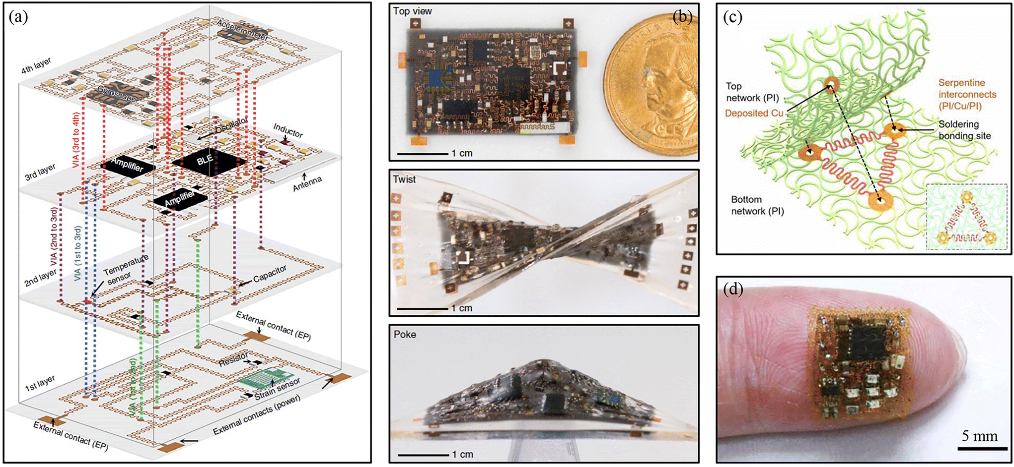 | ||
| Fig. 5 Transfer printing for 3D integrated soft electronics. (a) Schematic of a 3D integrated stretchable circuit. (b) Optical image of a four-layer stretchable circuit in unstretched, twist, and poke states. Reproduced from ref. 112 with permission from the Nature Publishing Group, copyright 2018. (c) Schematic of a 3D integrated soft system packed with a network material. (d) Optical image of a network material-based three-layer stretchable circuit. Reproduced from ref. 115 with permission from the American Association for the Advancement of Science, copyright 2022. | ||
Conclusions and future outlook
This paper presents a brief review of transfer printing technology for soft electronics. Transfer printing provides reliable routes to assemble nanomaterials into well-designed and controllable 2D and 3D architectures, construct curvy electronics with conformable stamps, build bioelectronics for various applications, and achieve the assembly of high-density components with 3D integrated technology. Among the wide range of opportunities for transfer printing technology, one may focus on studying more controllable protocols to achieve high complexity, high resolution, and low numbers of defects. The interfacial adhesion, modulated by surface physics or chemistry, and methods assisted by other factors (glue, light, etc.) need to be extensively studied. Strategies for soft devices in nanoscale, with greater integration and better stability, should be improved. Second, transfer printing techniques for 3D integrated soft electronics should be further developed to increase the function density and system stability. The existing laser etching method can achieve vertical interconnect access over tens of micrometers, which cannot satisfy the electrical interconnection of devices at the micro/nanoscale. Mechanical coupling between layers in the 3D integrated device and the strain isolation method should be studied further to increase system stretchability. As previously transferred layers have distortion during the printing process, future transfer printing techniques should be able to extend the advanced interlayer alignment process for 3D soft electronics. Third, programmable stamps with actively controlled surfaces may be established for curve electronics or other configurations. Though curvy electronics could be constructed with the CAS printing technique, it is only applicable to relatively regular surfaces such as spherical surfaces. More advanced stamps should be developed to satisfy other surfaces with complex geometries for artificial robots or biological applications. Finally, it is still challenging to develop industry-compatible manufacturing processes and equipment for large-scale and high-yield products of soft electronics. Transfer printing technology is incompatible with conventional fabrication processes. The uniformity and stability of samples demonstrated in the laboratory cannot satisfy application research on a large scale. Transfer printing processes and standards for mass production need to be studied.Author contributions
Z. H. and Y. L. investigated the literature and assembled the figures. Z. H. wrote the original draft. Z. H. and Y. L. revised the manuscript.Conflicts of interest
There are no conflicts to declare.Acknowledgements
This work was supported by the National Natural Science Foundation of China under grant numbers 61825102 and U21A20460, the Fundamental Research Funds for the Central Universities of UESTC under grant number ZYGX2021YGLH002 (Y. L.), the Shenzhen Science and Technology Planning Project (JSGG20201102152403008), the Science and Technology Project of Shenzhen City (JSGG20210802154213040), and the Project of Innovation and Strong School (PT2020C002).References
- W. Gao, S. Emaminejad, H. Y. Y. Nyein, S. Challa, K. Chen, A. Peck, H. M. Fahad, H. Ota, H. Shiraki, D. Kiriya, D.-H. Lien, G. A. Brooks, R. W. Davis and A. Javey, Nature, 2016, 529, 509–514 CrossRef CAS PubMed.
- H.-R. Lim, H. S. Kim, R. Qazi, Y.-T. Kwon, J.-W. Jeong and W.-H. Yeo, Adv. Mater., 2020, 32, 1901924 CrossRef CAS PubMed.
- G.-H. Lee, H. Moon, H. Kim, G. H. Lee, W. Kwon, S. Yoo, D. Myung, S. H. Yun, Z. Bao and S. K. Hahn, Nat. Rev. Mater., 2020, 5, 149–165 CrossRef PubMed.
- S. Niu, N. Matsuhisa, L. Beker, J. Li, S. Wang, J. Wang, Y. Jiang, X. Yan, Y. Yun, W. Burnett, A. S. Y. Poon, J. B. H. Tok, X. Chen and Z. Bao, Nat. Electron., 2019, 2, 361–368 CrossRef.
- Y. Yu, J. Nassar, C. Xu, J. Min, Y. Yang, A. Dai, R. Doshi, A. Huang, Y. Song, R. Gehlhar, A. D. Ames and W. Gao, Sci. Rob., 2020, 5, eaaz7946 CrossRef PubMed.
- J. Wang, M.-F. Lin, S. Park and P. S. Lee, Mater. Today, 2018, 21, 508–526 CrossRef.
- W. Heng, S. Solomon and W. Gao, Adv. Mater., 2022, 34, 2107902 CrossRef CAS PubMed.
- B. Llerena Zambrano, A. F. Renz, T. Ruff, S. Lienemann, K. Tybrandt, J. Vörös and J. Lee, Adv. Healthcare Mater., 2021, 10, 2001397 CrossRef CAS PubMed.
- D. H. Keum, S.-K. Kim, J. Koo, G.-H. Lee, C. Jeon, J. W. Mok, B. H. Mun, K. J. Lee, E. Kamrani, C.-K. Joo, S. Shin, J.-Y. Sim, D. Myung, S. H. Yun, Z. Bao and S. K. Hahn, Sci. Adv., 2020, 6, eaba3252 CrossRef CAS PubMed.
- P. Li, G.-H. Lee, S. Y. Kim, S. Y. Kwon, H.-R. Kim and S. Park, ACS Nano, 2021, 15, 1960–2004 CrossRef CAS PubMed.
- H. Yuk, B. Lu, S. Lin, K. Qu, J. Xu, J. Luo and X. Zhao, Nat. Commun., 2020, 11, 1604 CrossRef CAS PubMed.
- R. Herbert, H.-R. Lim, S. Park, J.-H. Kim and W.-H. Yeo, Adv. Healthcare Mater., 2021, 10, 2100158 CrossRef CAS PubMed.
- S. P. Sreenilayam, I. Ul Ahad, V. Nicolosi and D. Brabazon, Mater. Today, 2021, 43, 99–131 CrossRef CAS.
- N. Zhou, Y. Bekenstein, C. N. Eisler, D. Zhang, A. M. Schwartzberg, P. Yang, A. P. Alivisatos and J. A. Lewis, Sci. Adv., 2019, 5, eaav8141 CrossRef CAS PubMed.
- A. Carlson, A. M. Bowen, Y. Huang, R. G. Nuzzo and J. A. Rogers, Adv. Mater., 2012, 24, 5284–5318 CrossRef CAS PubMed.
- C. Linghu, S. Zhang, C. Wang and J. Song, npj Flexible Electron., 2018, 2, 26 CrossRef.
- H. Zhou, W. Qin, Q. Yu, H. Cheng, X. Yu and H. Wu, Nanomaterials, 2019, 9, 283 CrossRef CAS PubMed.
- M. A. Meitl, Z.-T. Zhu, V. Kumar, K. J. Lee, X. Feng, Y. Y. Huang, I. Adesida, R. G. Nuzzo and J. A. Rogers, Nat. Mater., 2006, 5, 33–38 CrossRef CAS.
- X. Feng, M. A. Meitl, A. M. Bowen, Y. Huang, R. G. Nuzzo and J. A. Rogers, Langmuir, 2007, 23, 12555–12560 CrossRef CAS PubMed.
- Z. Yan, T. Pan, M. Xue, C. Chen, Y. Cui, G. Yao, L. Huang, F. Liao, W. Jing, H. Zhang, M. Gao, D. Guo, Y. Xia and Y. Lin, Adv. Sci., 2017, 4, 1700251 CrossRef PubMed.
- D. S. Wie, Y. Zhang, M. K. Kim, B. Kim, S. Park, Y.-J. Kim, P. P. Irazoqui, X. Zheng, B. Xu and C. H. Lee, Proc. Natl. Acad. Sci. U. S. A., 2018, 115, E7236–E7244 CrossRef CAS PubMed.
- S. Heo, J. Ha, S. J. Son, I. S. Choi, H. Lee, S. Oh, J. Jekal, M. H. Kang, G. J. Lee, H. H. Jung, J. Yea, T. Lee, Y. Lee, J.-W. Choi, S. Xu, J. H. Choi, J.-W. Jeong, Y. M. Song, J.-C. Rah, H. Keum and K.-I. Jang, Sci. Adv., 2021, 7, eabh0040 CrossRef CAS PubMed.
- H. Luo, C. Li, C. Shi, S. Nie and J. Song, Theor. Appl. Mech. Lett., 2021, 11, 100308 CrossRef.
- A. Carlson, S. Wang, P. Elvikis, P. M. Ferreira, Y. Huang and J. A. Rogers, Adv. Funct. Mater., 2012, 22, 4476–4484 CrossRef CAS.
- S. Y. Yang, A. Carlson, H. Cheng, Q. Yu, N. Ahmed, J. Wu, S. Kim, M. Sitti, P. M. Ferreira, Y. Huang and J. A. Rogers, Adv. Mater., 2012, 24, 2117–2122 CrossRef CAS PubMed.
- H. Cheng, J. Wu, Q. Yu, H.-J. Kim-Lee, A. Carlson, K. T. Turner, K.-C. Hwang, Y. Huang and J. A. Rogers, Mech. Res. Commun., 2012, 43, 46–49 CrossRef.
- G.-H. Li, B.-L. Zhou, Z. Hou, Y.-F. Wei, R. Wen, T. Ji, Y. Wei, Y.-Y. Hao and Y.-X. Cui, Nanoscale Res. Lett., 2022, 17, 8 CrossRef CAS PubMed.
- J. W. Jeong, S. R. Yang, Y. H. Hur, S. W. Kim, K. M. Baek, S. Yim, H.-I. Jang, J. H. Park, S. Y. Lee, C.-O. Park and Y. S. Jung, Nat. Commun., 2014, 5, 5387 CrossRef CAS PubMed.
- B. Jeong, I. Hwang, S. H. Cho, E. H. Kim, S. Cha, J. Lee, H. S. Kang, S. M. Cho, H. Choi and C. Park, ACS Nano, 2016, 10, 9026–9035 CrossRef CAS PubMed.
- R. Saeidpourazar, M. D. Sangid, J. A. Rogers and P. M. Ferreira, J. Manuf. Process., 2012, 14, 416–424 CrossRef.
- H. Luo, C. Wang, C. Linghu, K. Yu, C. Wang and J. Song, Natl. Sci. Rev., 2019, 7, 296–304 CrossRef PubMed.
- H. Luo, S. Wang, C. Wang, C. Linghu and J. Song, Adv. Funct. Mater., 2021, 31, 2010297 CrossRef CAS.
- K.-I. Jang, K. Li, H. U. Chung, S. Xu, H. N. Jung, Y. Yang, J. W. Kwak, H. H. Jung, J. Song, C. Yang, A. Wang, Z. Liu, J. Y. Lee, B. H. Kim, J.-H. Kim, J. Lee, Y. Yu, B. J. Kim, H. Jang, K. J. Yu, J. Kim, J. W. Lee, J.-W. Jeong, Y. M. Song, Y. Huang, Y. Zhang and J. A. Rogers, Nat. Commun., 2017, 8, 15894 CrossRef CAS PubMed.
- Y. Park, C. K. Franz, H. Ryu, H. Luan, K. Y. Cotton, J. U. Kim, T. S. Chung, S. Zhao, A. Vazquez-Guardado, D. S. Yang, K. Li, R. Avila, J. K. Phillips, M. J. Quezada, H. Jang, S. S. Kwak, S. M. Won, K. Kwon, H. Jeong, A. J. Bandodkar, M. Han, H. Zhao, G. R. Osher, H. Wang, K. Lee, Y. Zhang, Y. Huang, J. D. Finan and J. A. Rogers, Sci. Adv., 2021, 7, eabf9153 CrossRef CAS PubMed.
- W. Cao, G. Liu, J. Miao, G. Zhang, J. Cui, Y. Yang, C. He, W. Zhang and R. Wang, Micromachines, 2021, 12, 1255 CrossRef PubMed.
- F.-C. Liang, Y.-W. Chang, C.-C. Kuo, C.-J. Cho, D.-H. Jiang, F.-C. Jhuang, S.-P. Rwei and R. Borsali, Nanoscale, 2019, 11, 1520–1530 RSC.
- B. H. Kim, M. S. Onses, J. B. Lim, S. Nam, N. Oh, H. Kim, K. J. Yu, J. W. Lee, J.-H. Kim, S.-K. Kang, C. H. Lee, J. Lee, J. H. Shin, N. H. Kim, C. Leal, M. Shim and J. A. Rogers, Nano Lett., 2015, 15, 969–973 CrossRef CAS PubMed.
- B. H. Kim, S. Nam, N. Oh, S.-Y. Cho, K. J. Yu, C. H. Lee, J. Zhang, K. Deshpande, P. Trefonas, J.-H. Kim, J. Lee, J. H. Shin, Y. Yu, J. B. Lim, S. M. Won, Y. K. Cho, N. H. Kim, K. J. Seo, H. Lee, T.-i. Kim, M. Shim and J. A. Rogers, ACS Nano, 2016, 10, 4920–4925 CrossRef CAS PubMed.
- P. Yang, L. Zhang, D. J. Kang, R. Strahl and T. Kraus, Adv. Opt. Mater., 2020, 8, 1901429 CrossRef CAS.
- T. Meng, Y. Zheng, D. Zhao, H. Hu, Y. Zhu, Z. Xu, S. Ju, J. Jing, X. Chen, H. Gao, K. Yang, T. Guo, F. Li, J. Fan and L. Qian, Nat. Photonics, 2022, 16, 297–303 CrossRef CAS.
- S. H. Lee, T. I. Lee, M.-H. Ham, S. J. Lee, J. H. Park, Y. C. Kim, P. Biswas and J. M. Myoung, Adv. Funct. Mater., 2015, 25, 6921–6926 CrossRef CAS.
- T.-A. Pham, T.-K. Nguyen, R. K. Vadivelu, T. Dinh, A. Qamar, S. Yadav, Y. Yamauchi, J. A. Rogers, N.-T. Nguyen and H.-P. Phan, Adv. Funct. Mater., 2020, 30, 2004655 CrossRef CAS.
- H. Jiang, D.-Y. Khang, J. Song, Y. Sun, Y. Huang and J. A. Rogers, Proc. Natl. Acad. Sci. U. S. A., 2007, 104, 15607–15612 CrossRef CAS PubMed.
- S. Xu, Z. Yan, K.-I. Jang, W. Huang, H. Fu, J. Kim, Z. Wei, M. Flavin, J. McCracken, R. Wang, A. Badea, Y. Liu, D. Xiao, G. Zhou, J. Lee, H. U. Chung, H. Cheng, W. Ren, A. Banks, X. Li, U. Paik, R. G. Nuzzo, Y. Huang, Y. Zhang and J. A. Rogers, Science, 2015, 347, 154–159 CrossRef CAS PubMed.
- Y. Gu, C. Wang, N. Kim, J. Zhang, T. M. Wang, J. Stowe, R. Nasiri, J. Li, D. Zhang, A. Yang, L. H.-H. Hsu, X. Dai, J. Mu, Z. Liu, M. Lin, W. Li, C. Wang, H. Gong, Y. Chen, Y. Lei, H. Hu, Y. Li, L. Zhang, Z. Huang, X. Zhang, S. Ahadian, P. Banik, L. Zhang, X. Jiang, P. J. Burke, A. Khademhosseini, A. D. McCulloch and S. Xu, Nat. Nanotechnol., 2022, 17, 292–300 CrossRef CAS PubMed.
- J. Park, J. Kim, S.-Y. Kim, W. H. Cheong, J. Jang, Y.-G. Park, K. Na, Y.-T. Kim, J. H. Heo, C. Y. Lee, J. H. Lee, F. Bien and J.-U. Park, Sci. Adv., 2018, 4, eaap9841 CrossRef PubMed.
- J. Kim, J. Park, Y.-G. Park, E. Cha, M. Ku, H. S. An, K.-P. Lee, M.-I. Huh, J. Kim, T.-S. Kim, D. W. Kim, H. K. Kim and J.-U. Park, Nat. Biomed. Eng., 2021, 5, 772–782 CrossRef PubMed.
- Y. M. Song, Y. Xie, V. Malyarchuk, J. Xiao, I. Jung, K.-J. Choi, Z. Liu, H. Park, C. Lu, R.-H. Kim, R. Li, K. B. Crozier, Y. Huang and J. A. Rogers, Nature, 2013, 497, 95–99 CrossRef CAS PubMed.
- M. Kim, G. J. Lee, C. Choi, M. S. Kim, M. Lee, S. Liu, K. W. Cho, H. M. Kim, H. Cho, M. K. Choi, N. Lu, Y. M. Song and D.-H. Kim, Nat. Electron., 2020, 3, 546–553 CrossRef.
- M. Lee, G. J. Lee, H. J. Jang, E. Joh, H. Cho, M. S. Kim, H. M. Kim, K. M. Kang, J. H. Lee, M. Kim, H. Jang, J.-E. Yeo, F. Durand, N. Lu, D.-H. Kim and Y. M. Song, Nat. Electron., 2022, 5, 452–459 CrossRef.
- B. Tian, J. Liu, T. Dvir, L. Jin, J. H. Tsui, Q. Qing, Z. Suo, R. Langer, D. S. Kohane and C. M. Lieber, Nat. Mater., 2012, 11, 986–994 CrossRef CAS PubMed.
- W. Xu, Z. Qin, C.-T. Chen, H. R. Kwag, Q. Ma, A. Sarkar, M. J. Buehler and D. H. Gracias, Sci. Adv., 2017, 3, e1701084 CrossRef PubMed.
- Y. Liu, B. Shaw, M. D. Dickey and J. Genzer, Sci. Adv., 2017, 3, e1602417 CrossRef PubMed.
- W. L. Noorduin, A. Grinthal, L. Mahadevan and J. Aizenberg, Science, 2013, 340, 832–837 CrossRef CAS PubMed.
- B. Tian, T. Cohen-Karni, Q. Qing, X. Duan, P. Xie and C. M. Lieber, Science, 2010, 329, 830–834 CrossRef CAS PubMed.
- D.-M. Sun, M. Y. Timmermans, A. Kaskela, A. G. Nasibulin, S. Kishimoto, T. Mizutani, E. I. Kauppinen and Y. Ohno, Nat. Commun., 2013, 4, 2302 CrossRef PubMed.
- S. Kim, N. Liu and A. A. Shestopalov, ACS Nano, 2022, 16, 6134–6144 CrossRef CAS PubMed.
- W. Xu, Y. Huang, X. Zhao, X. Jiang, T. Yang and H. Zhu, Nano Sel., 2021, 2, 121–128 CrossRef CAS.
- M. A. Skylar-Scott, J. Mueller, C. W. Visser and J. A. Lewis, Nature, 2019, 575, 330–335 CrossRef CAS PubMed.
- Y. Xu, G. Zhao, L. Zhu, Q. Fei, Z. Zhang, Z. Chen, F. An, Y. Chen, Y. Ling, P. Guo, S. Ding, G. Huang, P.-Y. Chen, Q. Cao and Z. Yan, Proc. Natl. Acad. Sci. U. S. A., 2020, 117, 18292–18301 CrossRef CAS PubMed.
- N. Yi, Y. Gao, A. Lo Verso, J. Zhu, D. Erdely, C. Xue, R. Lavelle and H. Cheng, Mater. Today, 2021, 50, 24–34 CrossRef CAS PubMed.
- W. Zhang, L. Zhang, Y. Liao and H. Cheng, Int. J. Extreme Manuf., 2021, 3, 042001 CrossRef CAS.
- E. K. Lee, R. K. Baruah, J. W. Leem, W. Park, B. H. Kim, A. Urbas, Z. Ku, Y. L. Kim, M. A. Alam and C. H. Lee, Adv. Mater., 2020, 32, 2004456 CrossRef CAS PubMed.
- Z. Rao, Y. Lu, Z. Li, K. Sim, Z. Ma, J. Xiao and C. Yu, Nat. Electron., 2021, 4, 513–521 CrossRef.
- K. Sim, S. Chen, Z. Li, Z. Rao, J. Liu, Y. Lu, S. Jang, F. Ershad, J. Chen, J. Xiao and C. Yu, Nat. Electron., 2019, 2, 471–479 CrossRef CAS.
- Y. J. Hong, H. Jeong, K. W. Cho, N. Lu and D.-H. Kim, Adv. Funct. Mater., 2019, 29, 1808247 CrossRef.
- S. Zhang, S. Li, Z. Xia and K. Cai, J. Mater. Chem. B, 2020, 8, 852–862 RSC.
- Y. Ma, Y. Zhang, S. Cai, Z. Han, X. Liu, F. Wang, Y. Cao, Z. Wang, H. Li, Y. Chen and X. Feng, Adv. Mater., 2020, 32, 1902062 CrossRef CAS PubMed.
- J.-W. Jeong, W.-H. Yeo, A. Akhtar, J. J. S. Norton, Y.-J. Kwack, S. Li, S.-Y. Jung, Y. Su, W. Lee, J. Xia, H. Cheng, Y. Huang, W.-S. Choi, T. Bretl and J. A. Rogers, Adv. Mater., 2013, 25, 6839–6846 CrossRef CAS PubMed.
- P. Wu, A. Xiao, Y. Zhao, F. Chen, M. Ke, Q. Zhang, J. Zhang, X. Shi, X. He and Y. Chen, Nanoscale, 2019, 11, 21103–21118 RSC.
- G. Yao, X. Mo, C. Yin, W. Lou, Q. Wang, S. Huang, L. Mao, S. Chen, K. Zhao, T. Pan, L. Huang and Y. Lin, Sci. Adv., 2022, 8, eabl8379 CrossRef CAS PubMed.
- Y. Liu, J. Liu, S. Chen, T. Lei, Y. Kim, S. Niu, H. Wang, X. Wang, A. M. Foudeh, J. B. H. Tok and Z. Bao, Nat. Biomed. Eng., 2019, 3, 58–68 CrossRef CAS PubMed.
- C. Y. Kim, M. J. Ku, R. Qazi, H. J. Nam, J. W. Park, K. S. Nam, S. Oh, I. Kang, J.-H. Jang, W. Y. Kim, J.-H. Kim and J.-W. Jeong, Nat. Commun., 2021, 12, 535 CrossRef CAS PubMed.
- C. Liu, J.-T. Kim, S. S. Kwak, A. Hourlier-Fargette, R. Avila, J. Vogl, A. Tzavelis, H. U. Chung, J. Y. Lee, D. H. Kim, D. Ryu, K. B. Fields, J. L. Ciatti, S. Li, M. Irie, A. Bradley, A. Shukla, J. Chavez, E. C. Dunne, S. S. Kim, J. Kim, J. B. Park, H. H. Jo, J. Kim, M. C. Johnson, J. W. Kwak, S. R. Madhvapathy, S. Xu, C. M. Rand, L. E. Marsillio, S. J. Hong, Y. Huang, D. E. Weese-Mayer and J. A. Rogers, Adv. Healthcare Mater., 2021, 10, 2100383 CrossRef CAS PubMed.
- H. U. Chung, A. Y. Rwei, A. Hourlier-Fargette, S. Xu, K. Lee, E. C. Dunne, Z. Xie, C. Liu, A. Carlini, D. H. Kim, D. Ryu, E. Kulikova, J. Cao, I. C. Odland, K. B. Fields, B. Hopkins, A. Banks, C. Ogle, D. Grande, J. B. Park, J. Kim, M. Irie, H. Jang, J. Lee, Y. Park, J. Kim, H. H. Jo, H. Hahm, R. Avila, Y. Xu, M. Namkoong, J. W. Kwak, E. Suen, M. A. Paulus, R. J. Kim, B. V. Parsons, K. A. Human, S. S. Kim, M. Patel, W. Reuther, H. S. Kim, S. H. Lee, J. D. Leedle, Y. Yun, S. Rigali, T. Son, I. Jung, H. Arafa, V. R. Soundararajan, A. Ollech, A. Shukla, A. Bradley, M. Schau, C. M. Rand, L. E. Marsillio, Z. L. Harris, Y. Huang, A. Hamvas, A. S. Paller, D. E. Weese-Mayer, J. Y. Lee and J. A. Rogers, Nat. Med., 2020, 26, 418–429 CrossRef CAS PubMed.
- K. Lee, X. Ni, J. Y. Lee, H. Arafa, D. J. Pe, S. Xu, R. Avila, M. Irie, J. H. Lee, R. L. Easterlin, D. H. Kim, H. U. Chung, O. O. Olabisi, S. Getaneh, E. Chung, M. Hill, J. Bell, H. Jang, C. Liu, J. B. Park, J. Kim, S. B. Kim, S. Mehta, M. Pharr, A. Tzavelis, J. T. Reeder, I. Huang, Y. Deng, Z. Xie, C. R. Davies, Y. Huang and J. A. Rogers, Nat. Biomed. Eng., 2020, 4, 148–158 CrossRef PubMed.
- C. Wang, B. Qi, M. Lin, Z. Zhang, M. Makihata, B. Liu, S. Zhou, Y.-h. Huang, H. Hu, Y. Gu, Y. Chen, Y. Lei, T. Lee, S. Chien, K.-I. Jang, E. B. Kistler and S. Xu, Nat. Biomed. Eng., 2021, 5, 749–758 CrossRef CAS PubMed.
- C. Wang, X. Li, H. Hu, L. Zhang, Z. Huang, M. Lin, Z. Zhang, Z. Yin, B. Huang, H. Gong, S. Bhaskaran, Y. Gu, M. Makihata, Y. Guo, Y. Lei, Y. Chen, C. Wang, Y. Li, T. Zhang, Z. Chen, A. P. Pisano, L. Zhang, Q. Zhou and S. Xu, Nat. Biomed. Eng., 2018, 2, 687–695 CrossRef PubMed.
- C. Wang, X. Chen, L. Wang, M. Makihata, H.-C. Liu, T. Zhou and X. Zhao, Science, 2022, 377, 517–523 CrossRef CAS PubMed.
- J. Choi, A. J. Bandodkar, J. T. Reeder, T. R. Ray, A. Turnquist, S. B. Kim, N. Nyberg, A. Hourlier-Fargette, J. B. Model, A. J. Aranyosi, S. Xu, R. Ghaffari and J. A. Rogers, ACS Sens., 2019, 4, 379–388 CrossRef CAS PubMed.
- A. J. Bandodkar, P. Gutruf, J. Choi, K. Lee, Y. Sekine, J. T. Reeder, W. J. Jeang, A. J. Aranyosi, S. P. Lee, J. B. Model, R. Ghaffari, C.-J. Su, J. P. Leshock, T. Ray, A. Verrillo, K. Thomas, V. Krishnamurthi, S. Han, J. Kim, S. Krishnan, T. Hang and J. A. Rogers, Sci. Adv., 2019, 5, eaav3294 CrossRef PubMed.
- J. Kim, A. S. Campbell, B. E.-F. de Ávila and J. Wang, Nat. Biotechnol., 2019, 37, 389–406 CrossRef CAS PubMed.
- N. El-Atab, R. B. Mishra, F. Al-Modaf, L. Joharji, A. A. Alsharif, H. Alamoudi, M. Diaz, N. Qaiser and M. M. Hussain, Adv. Intell. Syst., 2020, 2, 2000128 CrossRef.
- C. De Pascali, G. A. Naselli, S. Palagi, R. B. N. Scharff and B. Mazzolai, Sci. Rob., 2022, 7, eabn4155 CrossRef PubMed.
- M. Li, A. Pal, A. Aghakhani, A. Pena-Francesch and M. Sitti, Nat. Rev. Mater., 2022, 7, 235–249 CrossRef PubMed.
- M. Nan, F. Wang, S. Kim, H. Li, Z. Jin, D. Bang, C.-S. Kim, J.-O. Park and E. Choi, Sens. Actuators, B, 2019, 301, 127127 CrossRef CAS.
- H. Jiang, L. Fan, S. Yan, F. Li, H. Li and J. Tang, Nanoscale, 2019, 11, 2231–2237 RSC.
- H. Joo, Y. Lee, J. Kim, J.-S. Yoo, S. Yoo, S. Kim, A. K. Arya, S. Kim, S. H. Choi, N. Lu, H. S. Lee, S. Kim, S.-T. Lee and D.-H. Kim, Sci. Adv., 2021, 7, eabd4639 CrossRef CAS PubMed.
- J. Zhang, J. Xu, J. Lim, J. K. Nolan, H. Lee and C. H. Lee, Adv. Healthcare Mater., 2021, 10, 2100194 CrossRef CAS PubMed.
- S. Hong, Y. Gu, J. K. Seo, J. Wang, P. Liu, Y. S. Meng, S. Xu and R. Chen, Sci. Adv., 5, eaaw0536 CrossRef CAS PubMed.
- Y. Fang, G. Chen, M. Bick and J. Chen, Chem. Soc. Rev., 2021, 50, 9357–9374 RSC.
- X. Yu, Z. Xie, Y. Yu, J. Lee, A. Vazquez-Guardado, H. Luan, J. Ruban, X. Ning, A. Akhtar, D. Li, B. Ji, Y. Liu, R. Sun, J. Cao, Q. Huo, Y. Zhong, C. Lee, S. Kim, P. Gutruf, C. Zhang, Y. Xue, Q. Guo, A. Chempakasseril, P. Tian, W. Lu, J. Jeong, Y. Yu, J. Cornman, C. Tan, B. Kim, K. Lee, X. Feng, Y. Huang and J. A. Rogers, Nature, 2019, 575, 473–479 CrossRef CAS PubMed.
- Y. H. Jung, J.-Y. Yoo, A. Vázquez-Guardado, J.-H. Kim, J.-T. Kim, H. Luan, M. Park, J. Lim, H.-S. Shin, C.-J. Su, R. Schloen, J. Trueb, R. Avila, J.-K. Chang, D. S. Yang, Y. Park, H. Ryu, H.-J. Yoon, G. Lee, H. Jeong, J. U. Kim, A. Akhtar, J. Cornman, T.-i. Kim, Y. Huang and J. A. Rogers, Nat. Electron., 2022, 5, 374–385 CrossRef.
- P. A. Lopes, B. C. Santos, A. T. de Almeida and M. Tavakoli, Nat. Commun., 2021, 12, 4666 CrossRef CAS PubMed.
- Y.-Q. Zheng, Y. Liu, D. Zhong, S. Nikzad, S. Liu, Z. Yu, D. Liu, H.-C. Wu, C. Zhu, J. Li, H. Tran, J. B.-H. Tok and Z. Bao, Science, 2021, 373, 88–94 CrossRef CAS PubMed.
- S. Wang, J. Xu, W. Wang, G.-J. N. Wang, R. Rastak, F. Molina-Lopez, J. W. Chung, S. Niu, V. R. Feig, J. Lopez, T. Lei, S.-K. Kwon, Y. Kim, A. M. Foudeh, A. Ehrlich, A. Gasperini, Y. Yun, B. Murmann, J. B. H. Tok and Z. Bao, Nature, 2018, 555, 83–88 CrossRef CAS PubMed.
- A. D. Mickle, S. M. Won, K. N. Noh, J. Yoon, K. W. Meacham, Y. Xue, L. A. McIlvried, B. A. Copits, V. K. Samineni, K. E. Crawford, D. H. Kim, P. Srivastava, B. H. Kim, S. Min, Y. Shiuan, Y. Yun, M. A. Payne, J. Zhang, H. Jang, Y. Li, H. H. Lai, Y. Huang, S.-I. Park, R. W. Gereau and J. A. Rogers, Nature, 2019, 565, 361–365 CrossRef CAS PubMed.
- Y. Zhang, A. D. Mickle, P. Gutruf, L. A. McIlvried, H. Guo, Y. Wu, J. P. Golden, Y. Xue, J. G. Grajales-Reyes, X. Wang, S. Krishnan, Y. Xie, D. Peng, C.-J. Su, F. Zhang, J. T. Reeder, S. K. Vogt, Y. Huang, J. A. Rogers and R. W. Gereau, Sci. Adv., 2019, 5, eaaw5296 CrossRef CAS PubMed.
- S. M. Won, E. Song, J. T. Reeder and J. A. Rogers, Cell, 2020, 181, 115–135 CrossRef CAS PubMed.
- J. Viventi, D.-H. Kim, L. Vigeland, E. S. Frechette, J. A. Blanco, Y.-S. Kim, A. E. Avrin, V. R. Tiruvadi, S.-W. Hwang, A. C. Vanleer, D. F. Wulsin, K. Davis, C. E. Gelber, L. Palmer, J. Van der Spiegel, J. Wu, J. Xiao, Y. Huang, D. Contreras, J. A. Rogers and B. Litt, Nat. Neurosci., 2011, 14, 1599–1605 CrossRef CAS PubMed.
- J. P. Seymour, F. Wu, K. D. Wise and E. Yoon, Microsyst. Nanoeng., 2017, 3, 16066 CrossRef PubMed.
- N. Li, Z. Yi, Y. Ma, F. Xie, Y. Huang, Y. Tian, X. Dong, Y. Liu, X. Shao, Y. Li, L. Jin, J. Liu, Z. Xu, B. Yang and H. Zhang, ACS Nano, 2019, 13, 2822–2830 CrossRef CAS PubMed.
- Z. Yi, F. Xie, Y. Tian, N. Li, X. Dong, Y. Ma, Y. Huang, Y. Hu, X. Xu, D. Qu, X. Lang, Z. Xu, J. Liu, H. Zhang and B. Yang, Adv. Funct. Mater., 2020, 30, 2000477 CrossRef CAS.
- Y. S. Choi, R. T. Yin, A. Pfenniger, J. Koo, R. Avila, K. Benjamin Lee, S. W. Chen, G. Lee, G. Li, Y. Qiao, A. Murillo-Berlioz, A. Kiss, S. Han, S. M. Lee, C. Li, Z. Xie, Y.-Y. Chen, A. Burrell, B. Geist, H. Jeong, J. Kim, H.-J. Yoon, A. Banks, S.-K. Kang, Z. J. Zhang, C. R. Haney, A. V. Sahakian, D. Johnson, T. Efimova, Y. Huang, G. D. Trachiotis, B. P. Knight, R. K. Arora, I. R. Efimov and J. A. Rogers, Nat. Biotechnol., 2021, 39, 1228–1238 CrossRef CAS PubMed.
- S.-K. Kang, L. Yin and C. Bettinger, MRS Bull., 2020, 45, 87–95 CrossRef CAS.
- W. B. Han, J. H. Lee, J.-W. Shin and S.-W. Hwang, Adv. Mater., 2020, 32, 2002211 CrossRef CAS PubMed.
- Y. Choi, J. Koo and J. A. Rogers, MRS Bull., 2020, 45, 103–112 CrossRef.
- Y. S. Choi, H. Jeong, R. T. Yin, R. Avila, A. Pfenniger, J. Yoo, J. Y. Lee, A. Tzavelis, Y. J. Lee, S. W. Chen, H. S. Knight, S. Kim, H.-Y. Ahn, G. Wickerson, A. Vázquez-Guardado, E. Higbee-Dempsey, B. A. Russo, M. A. Napolitano, T. J. Holleran, L. A. Razzak, A. N. Miniovich, G. Lee, B. Geist, B. Kim, S. Han, J. A. Brennan, K. Aras, S. S. Kwak, J. Kim, E. A. Waters, X. Yang, A. Burrell, K. San Chun, C. Liu, C. Wu, A. Y. Rwei, A. N. Spann, A. Banks, D. Johnson, Z. J. Zhang, C. R. Haney, S. H. Jin, A. V. Sahakian, Y. Huang, G. D. Trachiotis, B. P. Knight, R. K. Arora, I. R. Efimov and J. A. Rogers, Science, 2022, 376, 1006–1012 CrossRef CAS PubMed.
- G. Yao, L. Kang, C. Li, S. Chen, Q. Wang, J. Yang, Y. Long, J. Li, K. Zhao, W. Xu, W. Cai, Y. Lin and X. Wang, Proc. Natl. Acad. Sci. U. S. A., 2021, 118, e2100772118 CrossRef CAS PubMed.
- J. A. Rogers, T. Someya and Y. Huang, Science, 2010, 327, 1603–1607 CrossRef CAS PubMed.
- W. Wu, Sci. Technol. Adv. Mater., 2019, 20, 187–224 CrossRef CAS.
- Z. Huang, Y. Hao, Y. Li, H. Hu, C. Wang, A. Nomoto, T. Pan, Y. Gu, Y. Chen, T. Zhang, W. Li, Y. Lei, N. Kim, C. Wang, L. Zhang, J. W. Ward, A. Maralani, X. Li, M. F. Durstock, A. Pisano, Y. Lin and S. Xu, Nat. Electron., 2018, 1, 473–480 CrossRef.
- Q. Zhao, Z. Liang, B. Lu, Y. Chen, Y. Ma and X. Feng, Adv. Mater. Technol., 2018, 3, 1800169 CrossRef.
- K. Li, X. Cheng, F. Zhu, L. Li, Z. Xie, H. Luan, Z. Wang, Z. Ji, H. Wang, F. Liu, Y. Xue, C. Jiang, X. Feng, L. Li, J. A. Rogers, Y. Huang and Y. Zhang, Adv. Funct. Mater., 2019, 29, 1806630 CrossRef.
- H. Song, G. Luo, Z. Ji, R. Bo, Z. Xue, D. Yan, F. Zhang, K. Bai, J. Liu, X. Cheng, W. Pang, Z. Shen and Y. Zhang, Sci. Adv., 2022, 8, eabm3785 CrossRef CAS PubMed.
- D. Green Marques, P. Alhais Lopes, A. T. de Almeida, C. Majidi and M. Tavakoli, Lab Chip, 2019, 19, 897–906 RSC.
- S. Liu, D. S. Shah and R. Kramer-Bottiglio, Nat. Mater., 2021, 20, 851–858 CrossRef CAS PubMed.
- S. Biswas, A. Schoeberl, Y. Hao, J. Reiprich, T. Stauden, J. Pezoldt and H. O. Jacobs, Nat. Commun., 2019, 10, 4909 CrossRef PubMed.
| This journal is © The Royal Society of Chemistry 2022 |