
Copper inks for printed electronics: a review
Xianghui
Zeng
,
Pei
He
 *,
Minglu
Hu
,
Weikai
Zhao
,
Huitong
Chen
,
Longhui
Liu
,
Jia
Sun
and
Junliang
Yang
*
*,
Minglu
Hu
,
Weikai
Zhao
,
Huitong
Chen
,
Longhui
Liu
,
Jia
Sun
and
Junliang
Yang
*
Hunan Key Laboratory for Super-Microstructure and Ultrafast Process, School of Physics and Electronics, Central South University, Changsha, 410083, Hunan, People's Republic of China. E-mail: pei.he@csu.edu.cn; junliang.yang@csu.edu.cn
First published on 10th October 2022
Abstract
Conductive inks have attracted tremendous attention owing to their adaptability and the convenient large-scale fabrication. As a new type of conductive ink, copper-based ink is considered to be one of the best candidate materials for the conductive layer in flexible printed electronics owing to its high conductivity and low price, and suitability for large-scale manufacturing processes. Recently, tremendous progress has been made in the preparation of cooper-based inks for electronic applications, but the antioxidation ability of copper-based nanomaterials within inks or films, that is, long-term reliability upon exposure to water and oxygen, still needs more exploration. In this review, we present a comprehensive overview of copper inks for printed electronics from ink preparation, printing methods and sintering, to antioxidation strategies and electronic applications. The review begins with an overview of the development of copper inks, followed by a demonstration of various preparation methods for copper inks. Then, the diverse printing techniques and post-annealing strategies used to fabricate conductive copper patterns are discussed. In addition, antioxidation strategies utilized to stabilize the mechanical and electrical properties of copper nanomaterials are summarized. Then the diverse applications of copper inks for electronic devices, such as transparent conductive electrodes, sensors, optoelectronic devices, and thin-film transistors, are discussed. Finally, the future development of copper-based inks and the challenges of their application in printed electronics are discussed.
1. Introduction
The next-generation electronic devices (e-devices) are developing in the direction of wearables, and their advantages of light weight and portability are attracting increasing attention.1–3 The failure strain of monocrystalline silicon being less than 2%,4 so many silicon-based devices have poor ductility with high weight, which makes it difficult to adapt them to the requirements of flexibility and portability for wearable e-devices.5–7 At the same time, the high demand combined with the complexity of the traditional device preparation process make it difficult to achieve mass production at a low price.8–10 Printed electronics (PE) technology, which combines traditional printing technology with electronic manufacturing, often uses solution methods to prepare customized patterns through printing.11–13 Owing to the advantages of little waste of materials and a simple process, PE technology has been widely used in the large-scale preparation of electronic devices.14 Meanwhile, the printing process can be used to prepare electronic circuits and devices on different substrates, breaking the limitations of traditional silicon-based circuits, and the prepared devices have the characteristics of light weight, low cost, and bending resistance, promoting the development of the next generation of intelligent electronic devices.15–19Conductive inks are one of the most important functional materials in printed electronic devices, and their properties determine the methods of printing and annealing. In recent years, many conductive ink materials have been developed, such as graphene,20–23 carbon nanotubes,24–26 metal nanoparticles,27–29 and conductive polymers.30–32 Although organic polymers have good ductility and robustness, their conductivity is poor, necessitating additional fillers and doping to meet the application requirements. Graphene has no band gap, but only the ideal two-dimensional monolayer structure has good conductivity. In contrast, metallic materials with high intrinsic conductivity (Au ∼2.44 μΩ cm, Ag ∼1.59 μΩ cm, Cu ∼1.68 μΩ cm, Al ∼2.65 μΩ cm, Ni ∼6.99 μΩ cm) have great potential in low-power transmission and sensing.33 As an inert metal, gold generally does not react with other substances, and is widely used in TFTs and solar cells.34–37 However, its high price restricts its use for ink printing. As an alternative to gold, silver shows high conductivity and good fineness, and can be applied to a variety of printing methods,38,39 but its low electromigration resistance makes it prone to electromigration,40 resulting in long-term stability decline, and its price is relatively expensive. Copper is abundant (more than 1000 times the content of silver), cheap (1% of the price of silver), and shows good electrical conductivity (between those of silver and gold) and thermal conductivity.41–47
Copper-based inks are attracting increasing attention. A large number of studies have shown that copper-based inks can achieve high conductivity through printing, which is necessary to realize the industrialized preparation of large-scale flexible electronic devices.48–51 However, there are two obvious problems in copper-based inks, that is, the conductivity in the initial stage and long-term stability after preparation.52,53 There are many factors affecting the conductivity, such as the specific gravity of the metal filler, the bridging between single metal particles (nanowires), and the porosity of the sintered film.54–56 The stability is poor because copper is easily oxidized into copper oxide (CuO) and cuprous oxide (Cu2O) when placed in air.57–60 Therefore, how to prepare copper-based ink with low resistivity and strong oxidation resistance is a problem that people have been focusing on.
In recent years, copper-based ink has developed rapidly in the field of printing electronics, including the preparation of the ink, the improvement of the printing process, and new applications.61–66 To improve the electrical conductivity and stability of copper film after printing, many efforts have been made to modify the ink filler, adjust the printing mode, and optimize the sintering process.67–72 This review summarizes the recent work on copper-based inks, including the preparation and characteristics of common copper-based inks, and then the preparation of electronic devices through appropriate printing methods and sintering processes. In addition, we also introduce several methods to protect the printing plate from oxidation. Finally, we summarize the applications of copper-based ink, as shown in Fig. 1.
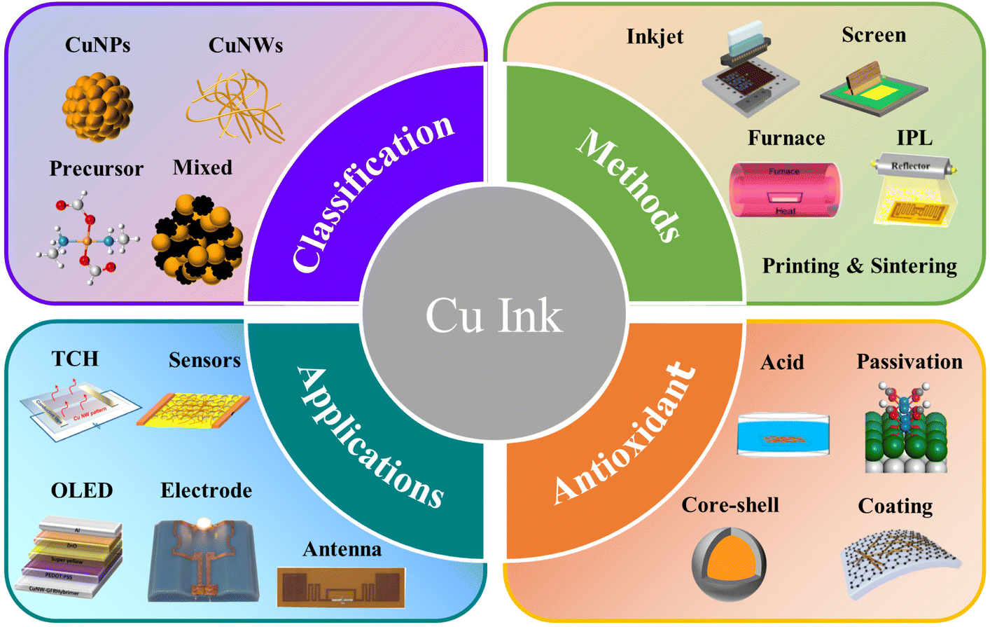 | ||
| Fig. 1 Schematic diagram of the classification, fabrication, antioxidation methods and application of copper inks. | ||
2. Preparation and properties of copper inks
Metal inks need to be sintered after printing to achieve neck connection between particles for conductivity. Compared with silver, the higher melting point of copper necessitates more energy during the sintering process.28,73 However, with the increase in temperature, the oxidation of copper seriously affects its conductivity, hindering its application as a high conductivity material. More importantly, flexible substrates (such as PET, PEN, and paper) cannot exist stably at high sintering temperatures (>150 °C). Thus, to realize sintering at lower temperatures (<120 °C) and solve the oxidation problem, copper-based inks with different formulations have been developed in previous research works.74–79 The different types of ink materials can be classified as follows: copper particle ink, copper nanowire ink, copper precursor ink, and copper mixed ink. This section discusses different formulations of copper inks and their performance.2.1. Copper particle ink
As one of the earliest developed materials, the preparation methods for metal particles are mature, such as chemical reduction, electrochemical synthesis, and thermal treatment.78,80–84 Micron or nanoscale particles show the unique properties of quantum size, but with the reduction of size, copper particles have a higher specific surface area, which means that they can be dispersed in solvents with a stabilizer to form conductive inks.85 However, for copper particles, small size will make more copper element exposed to water or oxygen to form oxides (CuO, Cu2O), which means that copper particle inks usually need to be stored in reducing solutions, such as oleic acid.86,87 More importantly, the higher melting point of copper oxide (CuO ∼1446 °C) will increase the temperature requirement for sintering. Although the synthesis of copper particles with a smaller radius can effectively reduce the temperature required for sintering,88,89 it will also make the particles agglomerate and precipitate in the solvent,56 resulting in nozzle blockage during the printing process. At present, the mainstream solution to increase the interaction between molecules and cover the copper particles to form a protective layer is to add capping agents of organic substances, such as polyvinylpyrrolidone (PVP),54,56,90–92 oleic acid,93 thiol,94,95 oleamine,96 cellulose97,98 and acid.76,99 The capping agents can be effectively desorbed during the subsequent sintering process, as shown in Fig. 2a. In addition, for different applications, additional additives (such as adhesives and surface tension modifiers) are needed to increase the adhesion between the ink and the substrate or change the shear adaptability of the ink.79 Information for several copper particle inks in terms of the materials, capping agents, sintering methods, and resistivity is listed in Table 1.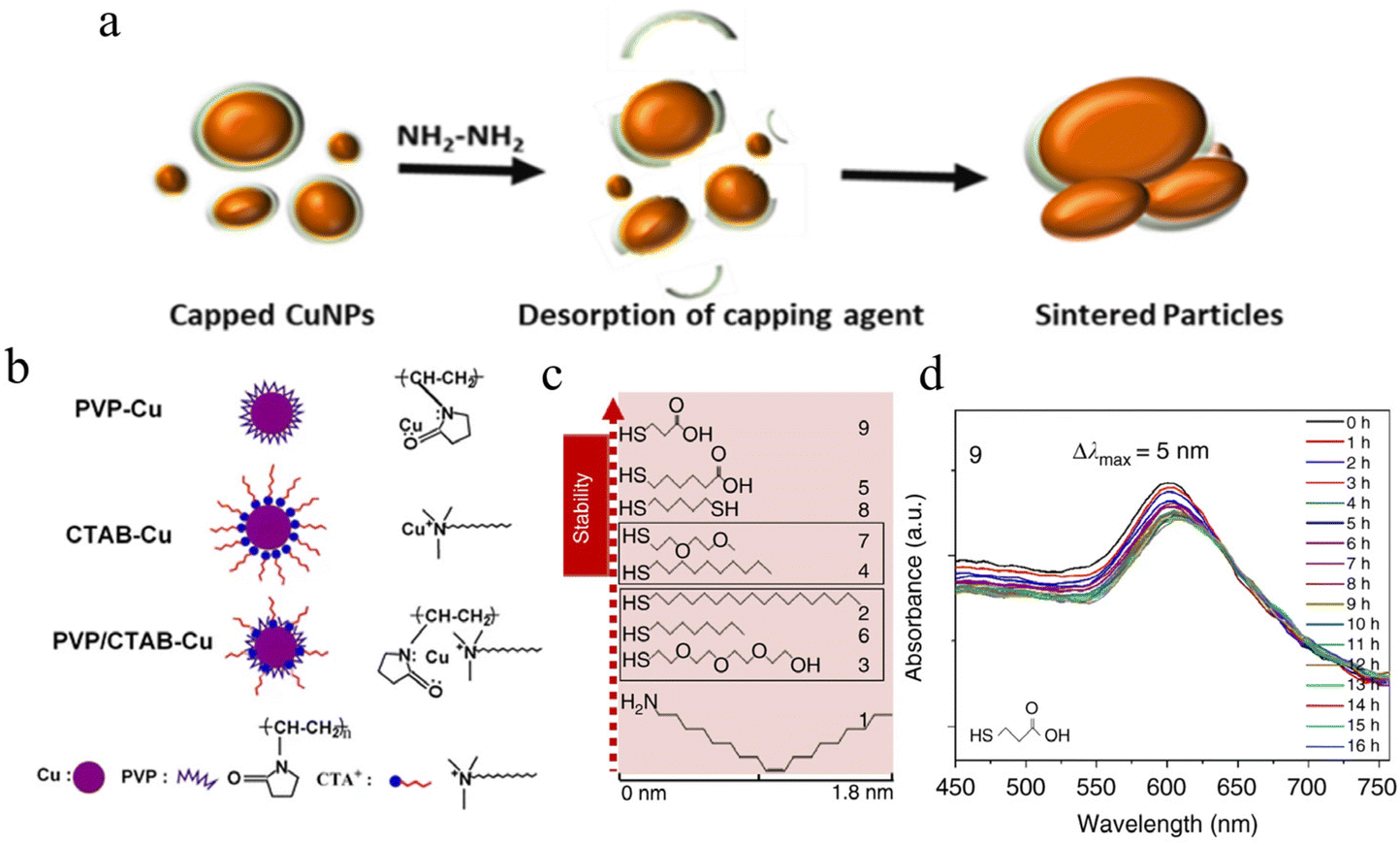 | ||
| Fig. 2 (a) Schematic diagram of high-molecular-weight PVP chemisorbed on the surface of CuNPs.76 Reproduced with permission from ref. 76. Copyright 2021 Elsevier. (b) The mechanism of PVP, CTAB, and the mix of PVP and CTAB with CuNPs.100 Reproduced with permission from ref. 100. Copyright 2013 Springer. (c) Molecular structures of thiols according to the stability in air when used as a capping layer for CuNPs.101 (d) The UV-vis stability of MPA-treated CuNPs.101 Reproduced with permission from ref. 101. Copyright 2017 Springer. | ||
| Material | Capping agent/reductant/additive | Substrate | Method | Post-treatment method | Resistivity (μΩ cm) | Ref. |
|---|---|---|---|---|---|---|
| Bulk Cu | — | — | — | — | 1.68 | |
| CuNPLs | HPMC | Kapton | Direct writing | Formate treatment | — | 97 |
| Cu flake | Phenol resin/triethanolamine | PI | Screen | Thermal sintering (170 °C in air) | 74.6 | 112 |
| CuNPs | Citric acid/sodium hypophosphite | PET | Screen | Thermal sintering (60 °C in air) | 744 ± 9 | 76 |
| CuNPs | NA | PI | Doctor balding | Thermal sintering (250 °C H2 in N2)/PECVD for graphene | 37.6 | 113 |
| CuNPs | EC/α-terpineol | PI | Screen | IPL | 9.54 | 114 |
| CuNPs | NA | GaAs | Inkjet | Laser sintering | 11 | 75 |
| CuNPs | PVP | Glass/PI | Spin-coating | Thermal sintering (225 °C in Ar) | 44.7 | 91 |
| CuNPs | 1-Octanethiol | Paper | Inkjet | IPL | 28 | 94 |
| CuNCs | BYK | Glass | Bar coating | Thermal sintering (400 °C in N2) | 23 | 74 |
| CuNPs | NA | Liquid crystal polymer | Aerosol jet | IPL | — | 115 |
| CuNPs | Copper acetate/2-dimethylaminoethanol | Si/SiO2 | Inkjet | Thermal sintering (250 °C in vacuum) | — | 116 |
| CuNPs | PGMEA | Si/SiO2 | EHD | Thermal sintering (380 °C in vacuum) | 8 × 10⁴ | 117 |
| CuNPs | 1-Octanethiol | PI | Inkjet | IPL | 24 | 95 |
| CuNPS | Oleic acid | PI | Air-brush | IPL | 6.7 | 93 |
| CuNPs | PVP/CTAB | Paper | Direct writing | Thermal sintering (160 °C in air) | 11 ± 0.8 | 100 |
| CuNPs | Lactic acid | Glass | Spin-coating | Thermal sintering (150 °C in N2) | 21.0 ± 7.0 | 99 |
| CuNPs | PVP | PI | Spin-coating | IPL | 5.2 | 54 |
| CuNPs | PVP | PI | Inkjet | Thermal sintering (275 °C in vacuum) | 11.6 | 90 |
| CuNPs | PVP/NaH2·PO2·H2O | Glass | Inkjet | Thermal sintering (325 °C in vacuum) | 17.2 | 56 |
| CuNPs | PVP/ascorbic acid | Si | Screen | Thermal sintering (400 °C in vacuum) | 27 | 118 |
| CuNPs/Ag | EC/α-terpineol | PET | Screen | Drying at room temperature | 14 | 98 |
| CuNPs/Ag | Oleylamine | Glass | Spin-coating | Thermal sintering (350 °C in vacuum) | 12.0 | 119 |
| CuNPs/Sn | Ascorbic acid | Scotch tape template | Spin-coating | Thermal sintering (200 °C in H2) | 164 | 120 |
| CuMPs/AgNPs | PVP/EG/glycerol | PET | Screen | IPL | — | 121 |
| CuNPs/CuNWs | PVP | PI | Spin-coating | Thermal sintering (250 °C in Ar) | 31.5 | 122 |
| Cu flake/NiF | AmIP/EG | PI | Doctor-blading | Thermal sintering (150 °C in N2) | 51 | 123 |
| CuNPs/Cu(NO3)2/Ni | PVP/DEG | PI | Doctor-blading | IPL | 14.78 | 124 |
| CuNPs/CuNWs | AMP/2-ethylhexylamine | PET | Screen | Thermal sintering (140 °C in N2) | 14.9 | 125 |
| CuNPs/CuMPs | EC/α-terpineol | PI | Screen | IPL | 5.94 | 126 |
| Cu(II) formate/Ni(II) formate | AMP | PI | Screen | Thermal sintering/IPL | 29 | 127 |
| CuNPs/CuMPs | EC | PI | Screen | IPL | 6.94 | 128 |
| CuMPs/AgNPs | EC/epoxy | PI | Screen | IPL | 5.12 | 129 |
| Cu(II) formate/MWCNT | AMP/n-octylamine | PET | Screen | Thermal sintering (140 °C in N2) | 25.31 | 130 |
| CuNPs/NiNPs | PVP/EC | PET | Screen | IPL | — | 131 |
| Cu@Sn NPs | Oleic acid | PES | Air-brush | IPL | 8.2 | 66 |
| Cu@Ni NPs | 2-Methoxy ethanol | Glass | Mayer coating | 350 °C in H2 and Ar | 27.4 | 68 |
| Cu@Ni NPs | Phenylhydrazine | PI | Spray-coating | IPL | — | 96 |
| Cu(II) formate/CuNPs | AMP | PET | Screen | Thermal sintering (140 °C in N2) | 11.3 | 132 |
| CuNPs/AgNPs | PVP | PI | Doctor-blading | IPL | 4.06 | 133 |
| Cu@Ag NPs | Oleylamine/1-amino-2-propanol | PET | Doctor-blading | Chemical sintering (MIPA and NaBH4) | 36.3 | 134 |
| Cu(II) formate/silver oxalate | EG/1,2-diaminopropane | PI | Dropping | 180 °C in N2 | 90.56 | 135 |
The chemical reduction generally uses substances such as ascorbic acid102 or hydrazine103,104 to reduce copper-containing compounds (Cu(NO3)2,105–107 Cu(HCOO)2,74 CuCl2,108–110etc.) to obtain elemental copper particles (CuPs). The capping agent can achieve chemisorption in solution through the interaction of lone electron pairs between N, O and Cu, forming a barrier between Cu and the outside environment (Fig. 2b).100 Jeong et al. synthesized copper nanoparticles (CuNPs) by polyol method, in which PVP with different molecular weights was added to the solution to control the thickness of the oxide layer on the surface of copper particles.90 Using PVP with a molecular weight of 40![[thin space (1/6-em)]](https://www.rsc.org/images/entities/char_2009.gif) 000 g mol−1, the synthesized copper particles had a diameter of 60 ± 8 nm and the minimum thickness of the CuO layer was 1.6 nm. PVP not only disperses the synthesized Cu particles evenly, but also improves the adhesion between the printed film and the substrate. Yokoyama et al. optimized the PVP concentration and dispersion time in the CuNPs ink and obtained the best dispersion effect and sufficiently high interface fracture energy at a concentration of 5 wt%.91 The sintering temperature was reduced to 225 °C and the resistivity of the film was 44.7 μΩ cm. Moreover, this ink can be applied to various substrates (glass, polyimide, polyaniline, liquid crystal polymer). However, the insulation of PVP affects the conductivity of the sintering pattern, and its high molecular weight means that its removal requires a high temperature,43 which is not applicable to substrates with a low glass transition temperature (Tg). Thus, it is necessary to find capping agents that can be decomposed at low temperature.111
000 g mol−1, the synthesized copper particles had a diameter of 60 ± 8 nm and the minimum thickness of the CuO layer was 1.6 nm. PVP not only disperses the synthesized Cu particles evenly, but also improves the adhesion between the printed film and the substrate. Yokoyama et al. optimized the PVP concentration and dispersion time in the CuNPs ink and obtained the best dispersion effect and sufficiently high interface fracture energy at a concentration of 5 wt%.91 The sintering temperature was reduced to 225 °C and the resistivity of the film was 44.7 μΩ cm. Moreover, this ink can be applied to various substrates (glass, polyimide, polyaniline, liquid crystal polymer). However, the insulation of PVP affects the conductivity of the sintering pattern, and its high molecular weight means that its removal requires a high temperature,43 which is not applicable to substrates with a low glass transition temperature (Tg). Thus, it is necessary to find capping agents that can be decomposed at low temperature.111
Short-chain carboxylic acids are regarded as good capping agents because of their good oxidation resistance and low decomposition temperature.136,137 The length of the carbon chain and the functional groups can affect the size and uniformity of the growth of copper particles. Longer carbon chains and more functional groups can improve the van der Waals interaction between molecules and produce greater cohesion, to obtain Cu with smaller particle size and better dispersion ablilty.138 Deng et al. prepared stable copper nanoparticles with particle sizes less than 10 nm with lactic acid as a capping agent.99 The low decomposition temperature of lactic acid enables the cooper ink to turn into Cu film with a resistivity of 21.0 ± 7.0 μΩ cm after annealing at 150 °C. They also found that increasing lactic acid concentration not only reduced the size of the synthesized copper particles, but also distributed the copper particles. However, with the addition of more acid, the pH of the ink will decrease, which will increase the copper reduction rate, and a large number of copper cores will rapidly accumulate, converge into large pie ces and harden.139 The purpose of capping is to make the capping agent form strong covalent bonds around Cu particles and hinder the agglomeration between particles and contact with oxygen. Therefore, in principle, a material that forms a strong covalent bond with copper is the best choice. Compared with copper–amine and copper–carboxylic acid bonds, copper–sulfur (Cu–S) bonds have stronger binding energy, so thiol solutions are the primary choice for capping.140 However, it is reported that thiol solution as a capping agent will etch CuNPS, making this scheme undesirable.141 Dabera et al. found for the first time that using mercaptan ligands with a short alkyl chain and containing hydrophilic carboxylic acid end groups can significantly reduce the oxidation rate of copper nanoparticles in the air without etching copper nanoparticles,101 as shown in Fig. 2d. The extinction spectrum of copper nanoparticles with 3-mercaptopropionic acid (MPA) only redshifted by 5 nm after being placed in air for 16 hours, showing high antioxidant performance. At the same time, the low boiling point of MPA (111.5 °C at 2.0 kPa) also greatly reduces the temperature required for sintering. High copper content copper particle inks can produce films with low resistivity after printing and sintering, but the addition of a capping agent and the use of reducing substances can only delay the oxidation process, which means that the copper particle ink often needs to be used immediately after preparation in the application process. This limits the convenience of use.
2.2. Copper nanowire ink
During the process of synthesizing copper particles, if the ligand is limited to binding specifically to other surfaces of copper, the nano copper will be guided to grow into one-dimensional nanowires along the uniaxial direction.41,44,48,50,142 Copper nanowires (CuNWs) have excellent mechanical toughness and an efficient electron transfer rate.143 The contact between rods without melting to form a neck connection significantly reduces the temperature required for sintering. CuNWs are generally synthesized in solution, using either the hydrothermal method or the organic solvent method depending on the solvent environment.144–146Table 2 lists the materials, capping agents, sintering methods, aspect ratio, and resistivity of some CuNWs inks.| Material | Capping agent/reductant | Length (μm) | Diameter (nm) | FoM | Sheet resistance (Ω sq−1) | Ref. |
|---|---|---|---|---|---|---|
| Cu(NO3)2 | EDA/hydrazine | 10 ± 3 | 90 ± 10 | 52.3 | 15 | 152 |
| CuCl2 | HDA/glucose | 35 | 50 | 72.3 | 25 | 147 |
| CuCl2 | HDA/glucose | 5–100 | 44.6 | 119.0 | 24 | 148 |
| CuCl2 | HDA/glucose | >50 | 66 ± 17 | NA | NA | 163 |
| CuCl2 | HDA, PVP/glucose | >100 | 28 ± 2.7 | 117 | 9.5 | 160 |
| CuCl2 | Oleylamine/ascorbic acid | 41.2 ± 22 | 100 ± 47 | 192.6 | 10.3 | 164 |
| CuCl2 | Oleylamine/tris(trimethylsilyl)silane | 10–20 | 21 ± 4 | 89.8 | 35 | 60 |
| CuCl2 | Oleylamine/ascorbic acid | 41.2 ± 22 | 115 ± 5 | 107.2 | 12.6 | 165 |
| CuCl2/Cu(acac)2 | Oleylamine/octadecene | 35–45 | 30–35 | 41.2 | 24.5 | 77 |
| CuCl2 | Oleylamine/ascorbic acid | 40 ± 21 | 134 ± 4 | 177.7 | 7.6 | 166 |
| CuCl2 | HDA/glucose | Aspect ratio | 1570 | 110.9 | 46 | 161 |
| CuCl2 | ODA/glucose | 38 ± 2 | 62 ± 14 | 48.5 | 35 | 167 |
| CuCl2 | HDA/WS2 | 70 | 11.3 | 154.3 | 28.5 | 162 |
| CuCl2 | HDA/glucose | 49.3 ± 19.9 | 45.4 ± 17.4 | 66.8 | 31 | 168 |
| CuCl2 | HDA/glucose | NA | 40 | 93.4 | 60 | 169 |
| CuCl2 | HDA/glucose | NA | 30 | 111.3 | 19 | 170 |
| CuCl2 | HDA/glucose | >100 | 36 | 80.9 | 34.05 | 171 |
| CuCl2 | HDA/glucose | NA | NA | 248.1 | 14.2 | 61 |
| CuCl2 | ODA/glucose | 20–50 | 30–90 | 79.8 | 20 | 155 |
| CuCl2 | HDA/glucose | 30 ± 13 | 36 ± 5 | 47.7 | 31.6 | 151 |
The hydrothermal method generally uses deionized water as the reaction medium, with hexadecylamine (HDA),147–151 ethylenediamine (EDA),152–154 octadecylamine (ODA)155–157 and PVP69,158,159 as the limiting ligand. By controlling the heating temperature, limiting ligand concentration and reaction time, CuNWs with different lengths and diameters can be obtained (Fig. 3a).152 Conductive networks composed of copper nanowires can be used to prepare transparent conductive films owing to the low duty cycle.50 Considering the superposition and entanglement of multiple nanowires in practical applications, such as transparent conductive films, it is often desirable to synthesize CuNWs with a small diameter and longer length. Zhong et al. synthesized well-dispersed CuNWs with an average diameter of 28 ± 2.7 nm and a length of several hundred microns by using HDA as the capping agent.160 HDA is a limiting ligand widely that is used in the synthesis of copper nanowires. It can be used as a capping agent for the synthesis of copper nanowires, and can also be used as a ligand to enhance the dispersion of copper nanowires and reduce the agglomeration of the nanowires, as shown in Fig. 3b.161 The diameter of CuNWs can be reduced by increasing the reaction temperature and ligand/reducing agent concentration. However, when the diameter is less than 30 nm, it is difficult for CuNWs to exist uniformly and stably due to the surface effect of the small-sized particl es.148 Kim et al. first proposed the synthesis of ultrafine CuNWs with an average diameter of 11.3 nm and length of 70μm using tungsten disulfide nanosheets as the catalytic reducing agent, copper chloride as the copper source, and HDA as the limiting ligand.162 As shown in Fig. 3c and d, HRTEM analysis showed that the CuNWs grew along the (110) direction, consistent with the conventional growth mode. This reveals the effectiveness of transition metal dichalcogenides (TMDs) in synthesizing metal nanowires.
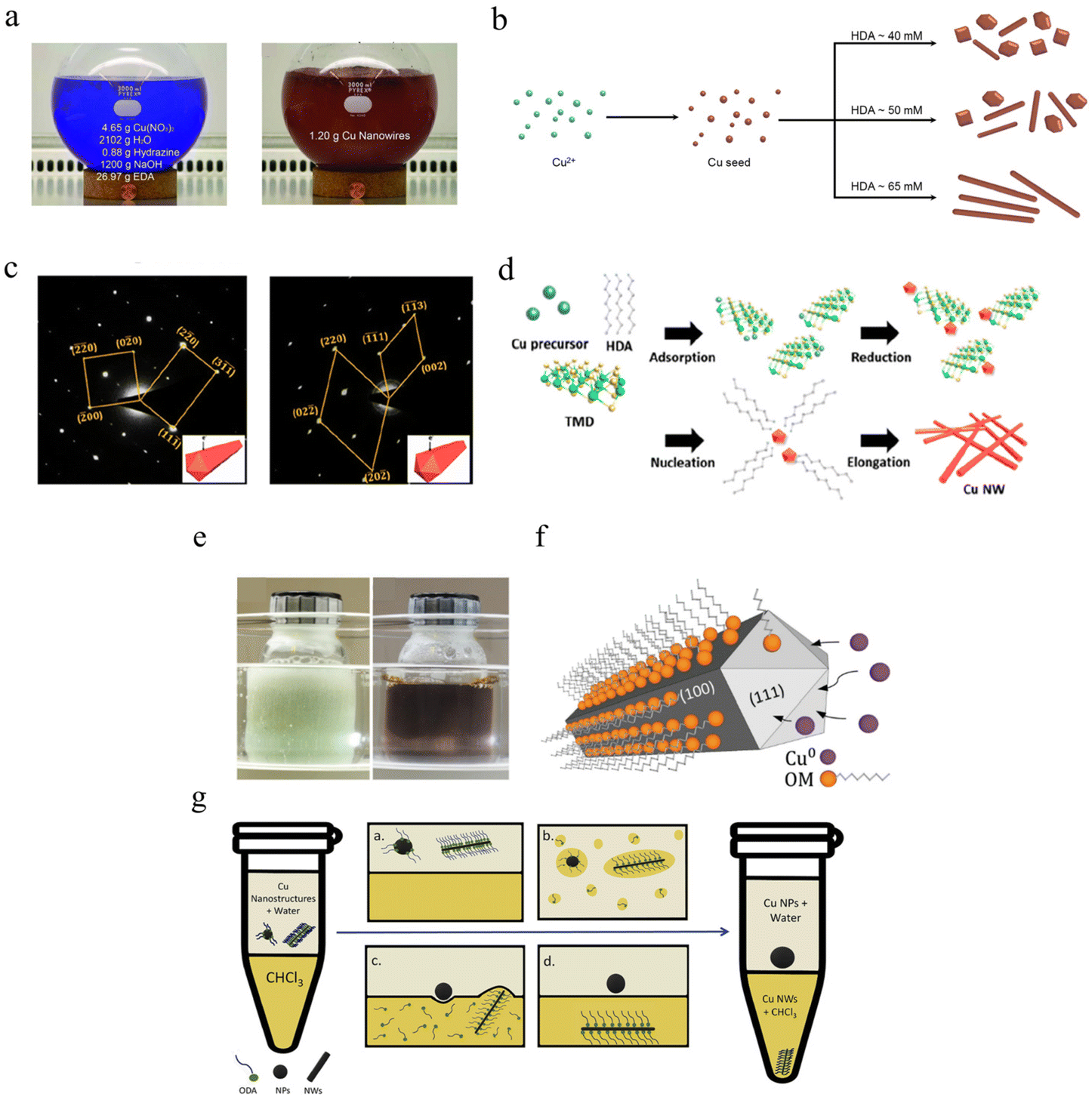 | ||
| Fig. 3 Synthesis of CuNWs. (a) Optical image of the hydrothermal method.152 Reproduced with permission from ref. 152. Copyright 2010 John Wiley and Sons. (b) Schematic image of the growth of CuNWs with different concentrations of HDA.161 Reproduced with permission from ref. 161. Copyright 2020 Springer. (c) SAED pattern of CuNWs with the incident beam perpendicular/parallel to one of the side facets.162 (d) Schematic illustration of the growth of CuNWs with WS2.162 Reproduced with permission from ref. 162. Copyright 2020 American Chemical Society. (e) Optical image of organic solvent methods.164 (f) Schematic of the formation of CuNWs using OM.164 Reproduced with permission from ref. 164. Copyright 2017 John Wiley and Sons. (g) Schematic diagram of the separation and purification CuNWs.167 Reproduced with permission from ref. 167. Copyright 2020 Elsevier. | ||
The organic solvent method is similar to that of aqueous phase synthesis. Notably, the organic solvent can not only be used as a reaction site but also as a limiting ligand to control the uniaxial growth of CuNWs.77,165,166 As shown in Fig. 3e, ascorbic acid (AA) was used as a reducing agent with oleylamine (OM) was the solvent and limiting ligand to guide the growth of CuNWs.164 Elemental copper, as a face-centered cubic (FCC) structure, exhibits the highest atomic packing density in the (111) direction. Therefore, OM tends to adsorb on the (100) surface with stronger surface activity, resulting in limited copper core growth in this direction, and finally guiding CuNWs to grow along the (110) direction (Fig. 3f). CuNWs are generally synthesized along with trace copper nanoparticles in the process, which can be effectively separated and purified by adding hydrophobic organic solvents. In addition, Hashimi et al. dispersed CuNWs in the organic phase by adding chloroform (CHCl3) to achieve the effect of separation and purification from CuNPs, as shown in Fig. 3g.167 The organic solvent residue needs to be removed by increasing the heating temperature. Meanwhile, excessive organic matter will affect the conductivity of the nanowires. Aqueous phase synthesis has the advantages of fast reaction, minimal residue, and convenient purification, which is widely used in experimental studies. Although CuNWs have excellent light transmittance and flexibility, electron scattering is intensified when the diameter is reduced to the mean free path of copper (40 nm), which usually makes the film produced by CuNWs much less conductive than film produced from dense sintered copper film.
2.3. Copper precursor ink
Copper precursor inks can decompose to produce elemental copper under the action of reducing agents by heating or light irradiation, while the ligands evaporate in the gaseous state. The existence of Cu(II) gives the ink the specific characteristics of long stability and easy processing, which effectively avoids the oxidation and precipitation of copper in the storage period, and greatly improves the convenience of Cu ink.127,172,173 Information on copper precursor inks in terms of the materials, reducing agents, sintering methods, and resistivity is listed in Table 3. Among previously reported Cu metal–organic decomposition (MOD) inks, copper formate (Cu(HCOO)2) is regarded as an ideal precursor material owing to its advantages of good oxidation resistance in air, low thermal decomposition temperature (150–250 °C), low amounts of residue and low price.174–176 Its decomposition equation is as follows: Cu(HCOO)2 → Cu + H2 + 2CO2 + H2O. In order to improve the processing efficiency of copper precursor ink, an amine ligand was introduced to provide central copper ions with electron-induced partial reduction of copper(II), which significantly reduced the temperature required for copper reduction. Since coordination can be formed in all six directions of the Cu(II) space, the configuration of the Cu complex changes from octahedron to square plane during the reduction process, and finally metal Cu is obtained.177 Kim et al. sintered copper foil with the lowest resistivity of 5.2 μΩ cm in a formic acid atmosphere by mixing copper formate and hexylamine, and pointed out that the content of hexamine affects the size distribution of copper particles (inverse ratio).178 Choi et al. compared the effect of different concentrations of hexylamine on copper nucleation and found that higher concentrations resulted in the formation of small CuNPs and less porous copper films, as shown in Fig. 4a.179 The role of hexylamine as a reducing and capping agent in the decomposition of copper precursor ink was confirmed, as shown in Fig. 4a. Compared with monoamine, diamine can be heated to produce imine, thus competing for O2 molecules on the active site of the copper surface to improve oxidation. Dong et al. used 1,2-diaminopropane (PDA) and copper formate as precursors and heated them directly in air to obtain a copper film with a resistivity of 18 μΩ cm.172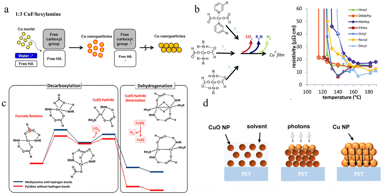 | ||
| Fig. 4 (a) Mechanism of reaction of different concentrations of hexylamine to produce CuNPs.179 Reproduced with permission from ref. 179. Copyright 2015 American Chemical Society. (b) Diagram of the decomposition temperature affected by hydrogen bonding of ligands (T1 < T2 < T3) and the resistivity of films formed by sintering various complexes.180 Reproduced with permission from ref. 180. Copyright 2018 Royal Society of Chemistry. (c) Schematic of the decomposition of copper formate with amine coordination.181 Reproduced with permission from ref. 181. Copyright 2020 American Chemical Society. (d) Schematic of the decomposition from CuO to Cu.182 Reproduced with permission from ref. 182. Copyright 2016 American Chemical Society. | ||
| Material | Reducing agent/ligand | Substrate | Method | Post-treatment method | Resistivity (μΩ cm) | Ref. |
|---|---|---|---|---|---|---|
| Cu(II) formate | Hexylamine | Glass | Mayer coating | 250 °C formic acid gas | 5.2 | 178 |
| Cu(II) formate | Hexylamine | Glass | Doctor-blading | 200 °C formic acid gas | 40.5 | 179 |
| Cu(II) formate | AMP | Glass | Inkjet | 190 °C N2 | 10.5 | 177 |
| Cu(II) formate | DPM | PI | Screen | IPL | NA | 173 |
| Cu(II) formate | PDA | PI | Spin-coating | 180 °C in air | 18 | 172 |
| Cu(II) formate | Dipropylamine/3-butylpyridine | Glass | NA | 95 °C in N2 | 8 | 188 |
| Cu(II) formate | 2-Ethyl-1-hexylamine | PI | Doctor-blading | 140 °C in N2 | 7 | 180 |
| Cu(II) formate | Pentylamine | Glass | NA | 110 °C in N2 | 5.7 | 175 |
| Cu(II) sulfate | NaBH4 | PI | Inkjet | Electroless plating | 5.68 | 189 |
| Cu(II) nitrate | EG | PDMS | Spin-coating | Laser | 90 | 190 |
| Cu ion | Formic acid, acetic acid/ammonia–water | PI | Inkjet | IPL | 2.3 | 191 |
| CuO | NA | Paper | Inkjet | IPL | 3.1 | 65 |
| CuO | EG | PET | Inkjet | IPL | 10 | 182 |
| CuO | EG | Glass | Spin-coating | Laser | 9.5 | 187 |
In the copper formate–amine complex, the decomposition temperature is determined by the interaction between hydrogen on the amine group and oxygen in the formate root (hydrogen bond); the size and porosity of the copper particles formed after sintering are also affected by the boiling point and coordination capacity of amine.183,184 Paquet et al. used a variety of amines to coordinate copper formate, and found that the decomposition temperature of copper formate gradually increased with the increase of hydrogen bonding.180 In addition, they also found that amines with a medium boiling point and strong coordination ability with the central copper ion (2-ethyl-1-hexylamine, octylamine and, decamine) can be sintered at low temperature to obtain good conductivity (140 °C,7 μΩ cm), which is due to the rapid volatilization of amines with low boiling points and weak coordination ability during sintering, resulting in uneven growth size and agglomeration of the copper cores (Fig. 4b). In general, the decomposition of amine-coordinated copper formate can be divided into the processes of ligand decarboxylation and dehydrogenation to produce CO2 and H2. Shin et al. analyzed the key role of the amine ligand in dehydrogenation and dehydrogenation of copper formate from a theoretical perspective, and found that the hydride dimer of Cu(II) self-reduced to produce a stable binuclear Cu(I) compound after dehydrogenation (Fig. 4c).181 Although Cu MOD ink is convenient, the low copper content in the solution results in relatively large resistance, and the generation of gas will also lead to pores in the film and affect the uniformity of film formation. In addition, CuO as a copper precursor ink can be used to improve the Cu content.65,185,186 Rahman et al. prepared Cu patterns (resistivity ranged from 9.5 to 71.6 μΩ cm) from commercial CuO ink using a green laser (532 nm).187 Rager et al. used CuO ink to prepare highly conductive Cu patterns (10 μΩ cm) on PET substrates; the CuO was reduced to Cu(0) under photonic radiation and grew into stable Cu patterns,182 as shown in Fig. 4d, in which the decomposition needs suitable reductants or high-energy irradiation to produce Cu(0).
2.4. Copper mixed ink
Copper films with uniform particle size and good connection between particles show higher conductivity and oxidation resistance. To improve the copper film quality, an extra conductive filler was added to the copper ink to increase the bridging property.55,66,121,128,129,135,192,193 As the growth of copper particles is affected by temperature, pH, ligand, and other factors in the process of sintering of precursor ink, it is difficult to form a uniform microstructure. Li et al. proposed to add an appropriate amount of submicron copper ‘seeds’ into the copper–amino complex to provide heterogeneous nucleation sites for self-reduction of copper precursor.132 In this method, a dense and thick copper conductive pattern with uniform microstructure and low resistivity (11.3 μΩ cm) was achieved, and the copper content in the ink was improved. Similarly, Jang et al. added CuNPs to the precursor ink of Cu(NO3)2 to improve the weldability between the particles, resulting in an electrode with a resistivity of 19.98 μΩ cm after flash sintering,124 as shown in Fig. 5a. In addition, adding conductive metal nanowires into copper precursor ink can change the growth of the copper cores from homogeneous to heterogeneous,125 which can control the growth of copper particles more closely arranged on the metal nanowire, resulting in the decomposition of copper precursors at low temperature (14.9 μΩ cm, sintering at 140 °C), as shown in Fig. 5b. | ||
| Fig. 5 (a) Schematic of adding CuNPs to Cu(NO3)2 for improving formation quality.124 Reproduced with permission from ref. 124. Copyright 2021 Springer. (b) Schematic of metal nanowires providing nucleation sites for CuNPs growth.125 Reproduced with permission from ref. 125. Copyright 2019 John Wiley and Sons. (c) Schematic of the decomposition/reduction of NiF-AmIP complex with Cu.123 (d) Cross-sectional elemental distribution maps of Cu and Ni.123 Reproduced with permission from ref. 123. Copyright 2021 American Chemical Society. | ||
Compared with precursor ink, copper particle ink requires a higher sintering temperature due to the copper cores melting, so the main improvement strategy is to add a metal filler with a lower melting point to copper particle ink.194 Chen et al. developed a copper–tin (Cu–Sn) mixed ink,131 and conductive copper film with sheet resistance of 14 Ω/sq was obtained by sintering metal nanoparticles with low photon energy. The excellent catalytic effect of copper can promote the self-reduction of other metal precursor inks, and the self-reduction nucleation of the filler metal can in turn promote the connection between the particles of copper ink after printing. Tomotoshi et al. took advantage of the catalytic effect of copper and added nickel formate and 1-amino-2-propanol complex (NiF-AMIP) into micron copper sheet to catalyze the in situ production of Ni at 150 °C in air to obtain a conductive film with a conductivity of 66 μΩ cm.123 The addition of copper reduces the temperature of NiF self-reduction and provides a site for Ni nucleation. In turn, the Ni attached to the growth of copper nuclei can form necking connections between copper particles, thus achieving high conductivity and isolation of the contact between copper and external H2O or O2, and improving the long-term stability of the printed film (the resistance increases by 1.8 times in 7 days at 80 °C and 80% RH), as shown in Fig. 5c and d. This method can be also used to prepare nanoparticles with core–shell structure by using the catalytic formation of nickel by copper,127 which showed excellent conductivity as low as 19 μΩ cm. In addition, CNT is also added to Cu ink to improve film unifromity.130,173,195 However, the resistivity of CNTs is higher than that of pure copper, thus the resistance of sintered pattern is increased. Although mixed copper ink has great advantages, including increasing the copper content of ink, improved ink film conductivity, and lower porosity, and its convenient storage condition and simple preparation technology for large-scale application, some conductive fillers (such as silver or nanoscale precious metals) are expensive, which is inconsistent with the starting point of the low price of copper.
3. Printing and sintering methods
Conventional processes (photolithography,196,197 vacuum deposition,198 etching,199etc.) have high requirements for equipment and harsh preparation conditions, which limit the application and large-scale preparation of electronic devices on different substrates, and cause more waste. Conductive ink adopts the additive manufacturing method because of its special rheological properties, which can be utilized to produce flexible and robust electronic devices on a variety of substrates through printing techniques.200–203 For the process of printing of electronic devices, the goal is to obtain qualified components or working circuits. Therefore, it is necessary to regulate the performance of ink according to the printing mode. For copper-based ink, the parameters to be controlled are viscosity, surface tension, copper content and particle size. The first two parameters limit the printing mode of the ink, while the latter two parameters affect the quality of the printed copper film. In this section, we will first introduce some printing processes applicable to copper-based ink and the basic requirements of this process for ink; the related information can be viewed in Table 4.71,117,142,207,218 Then we will introduce various methods for sintering; the related information can be viewed in Table 5.94,123,252,263,266| Printing process | Principle | Advantages | Drawbacks | Line width (μm) | Printing speed | Viscosity (cP) |
|---|---|---|---|---|---|---|
| Inkjet printing | Extrusion of droplets by piezoelectric deformation or thermal expansion | Low wastage of inks; good smoothness of ink trace; good operability | Clogging of nozzles; coffee-ring effect; satellite points; low adhesion | >10 | Moderate | 1–20 |
| Direct writing | Extrusion of inks through air pressure | Convenient operation; wide range of ink applications | Ink clogging causes printing discontinuity; high requirements for ink rheological performance | >500 | Moderate | 102–106 |
| EHD jet printing | Pull the inks by electric field force | Flexible operation; high printing efficiency; wide suitability of inks | Expensive instruments; complex operation | >0.1 | Low | 1–104 |
| Screen printing | Transfer ink from a screen plate to a substrate by scraper | Rapid large-scale production; easy operation; low-cost instruments | High roughness of ink trace; higher viscosity ink required | >30 | High | >500 |
| Sintering process | Principle | Advantages | Drawbacks | Operating conditions | Sintering speed |
|---|---|---|---|---|---|
| IPL sintering | Decomposition of organic capping agents and necking of copper particles due to light radiation | Convenient operation; quick completion; large scale; wide range of ink applications | Low resolution; concentrated energy in a short time | Ambient conditions | <10 ms |
| Laser sintering | Generating a hot spot in a very small area to achieve welding | Flexible operation; pattering[A51] | Expensive instruments; low sintering depth; low efficiency | Ambient conditions | <100 μs for each spot |
| Plasma sintering | Removal of organic matter using high-energy ions and electrons | Mild sintering temperature; flexible substrates can be stabilized | Expensive instruments; low efficiency; complex operating conditions; | Vacuum or low-pressure conditions | >10 min |
| Thermal sintering | Thermal decomposition of organic matter and reduction of copper oxide | Convenient operation; inexpensive instruments | High temperature destroys flexible substrate; oxidation is prone to occur; high porosity | Vacuum or inert gas conditions | 10–30 min |
| Chemical sintering | Reduction of acidic solutions | Simple operation; room-temperature processing; short time | Additional cleaning process; pollution; insignificant sintering effect | Ambient conditions | <1 min |
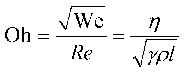
3.1. Printing conductive Cu ink
where η, ρ, γ, and l represent the viscosity, density and surface tension of the fluid, respectively, and l is the diameter of the nozzle.
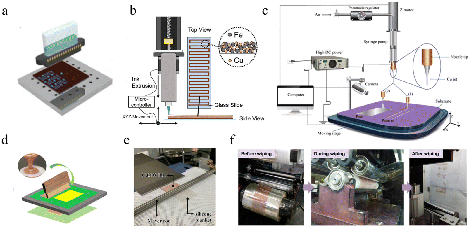 | ||
| Fig. 6 Printing methods for Cu inks. (a) Schematic of inkjet printing for CuNPs.209 Reproduced with permission from ref. 209. Copyright 2019 John Wiley and Sons. (b) Schematic of the fabrication of Cu–Fe mixed ink by direct writing.211 Reproduced with permission from ref. 211. Copyright 2020 Elsevier. (c) Schematic diagram showing EHD jet printing.117 Reproduced with permission from ref. 117. Copyright 2019 John Wiley and Sons. (d) Schematic illustration of screen printing.112 Reproduced with permission from ref. 112. Copyright 2022 Springer. (e) Optical image of Mayer rod for printing CuNWs ink.151 Reproduced with permission from ref. 151. Copyright 2022 American Chemical Society. (f) Optical image of large-scale R2R printing.212 Reproduced with permission from ref. 212. Copyright 2016 American Chemical Society. | ||
The dispersion stability of copper particles in ink is one of the key factors affecting whether the ink can be ejected from the nozzle. Excessive particle size and agglomeration between particles will block the nozzle. To achieve good printing ability, the size of copper particles should normally be less than a hundredth of the size of the nozzle diameter.142 Therefore, copper particles with large size or length are usually screened out through a filter before printing. To avoid nozzle clogging, Kim et al. reported a method for preparing conductive copper patterns by inkjet printing of copper sulfate and sodium phosphinate inks.206 Although inkjet printing has good operability and high resolution, owing to the low viscosity of the ink, the adhesion of the printed pattern to the substrate is a major problem. Moreover, the diffusion behavior of the ink on the substrate can also lead to the phenomenon of edge burrs and coffeering.208 To overcome this problem, an efficient route is modifying the printing substrate with a nanostructured self-assembly layer with 3-mercaptopropyltrimethoxysilane,191 which forms a silanol bond with the oxygen-treated PI film. The functional group on the other side forms a Cu–S bond with copper, which significantly enhances the adhesion of inkjet printing copper on PI. In addition, increasing the contact angle between the copper ink and the substrate can also increase the control of the printing pattern and reduce the disorder diffusion at the edge of the printed ink. Jun et al. pretreated the Si/SiO2 substrate with hexamethyldisilazane (HMDS), improved the contact angle of inkjet printing copper ink, and obtained a printing pattern with regular edges and no coffee-ring phenomenon.116 However, due to the entanglement of nanowires, there are few applications in inkjet printing.213–215
 , where C is the moving speed of the nozzle relative to the substrate.218 Owing to the existence of the forward contact angle, the line width will be slightly higher than l, so an effective way to improve the resolution is to increase the nozzle movement rate to close to the ink outflow rate or higher.
Similarly, Mayer rod coating uses gaps in the wire coiled around the bar to scrape off the excess solution,171,233,234 as shown in Fig. 6e. This technique can effectively control the thickness of the coating (about 1/10 of the wire diameter) and has a small footprint for direct application to R2R processes. Compared to screen and gravure printing, the ink has a lower additive content, so the resulting film performs better in terms of electrical conductivity.13,235
Printing resolution and printing rate have an inverse relationship. In general, to achieve high-resolution printing, non-contact digital printing techniques such as inkjet printing and EHD printing are good choices. They avoid direct contact with the substrate during printing, ensure the completeness of the ink, and achieve high precision printing. However, micro-processing manufacturing the printing rate slower and the cost of equipment is higher. Screen printing, gravure printing, spray-coating, and other non-digital printing methods can be done at high speed using a mask, but the disadvantage is that it is difficult to achieve high-resolution manufacturing (<10 μm). Recently, Kim et al. reported a reverse-offset printing technology,151 in which CuNWs were coated by Mayer rod and then transferred to a gravure plate. They used a commercial adhesive hand-roller to achieve the directional transfer of patterned ink to obtain CuNW patterns with a minimum line width of 7 μm. This printing method provides a potential solution for the rapid and efficient preparation of copper-based inks. To achieve high throughput and quality functional components, combining multiple printing methods may be an effective way to break the conflict between resolution and printing rate.
3.2. Sintering treatment methods
The preparation of conductive copper inks usually requires the addition of organic ligands such as capping agents and dispersants to improve the oxidation resistance and dispersibility of the ink. For conductivity, the covalent bonds between these fillers can restrict electron transfer and reduce film uniformity. Moreover, the high specific surface area of CuNPs will inevitably oxidize during preparation. Thus, it is necessary to employ an additional sintering process to remove these fillers to connect bare copper particles to achieve conductivity. There is an additional reductive decomposition process for copper precursors or copper mixed inks to guide the nucleation growth of copper or other conductive metal fillers.72 The quality of the sintered film can usually be measured in three aspects: (a) the degree of bridging between copper particles; (b) the porosity of the copper film; (c) the amount of oxide (CuO, Cu2O) and organic residue content. The more uniform the necking connection between copper particles, the smaller the film's porosity and the lower the amount of residue, which significantly improves the electrical conductivity of the sintered copper film. In order to improve the electrical properties of printed copper inks, various sintering processes have been developed, including photonic sintering, intense pulsed light (IPL) sintering, laser sintering, plasma sintering, thermal sintering, and chemical sintering.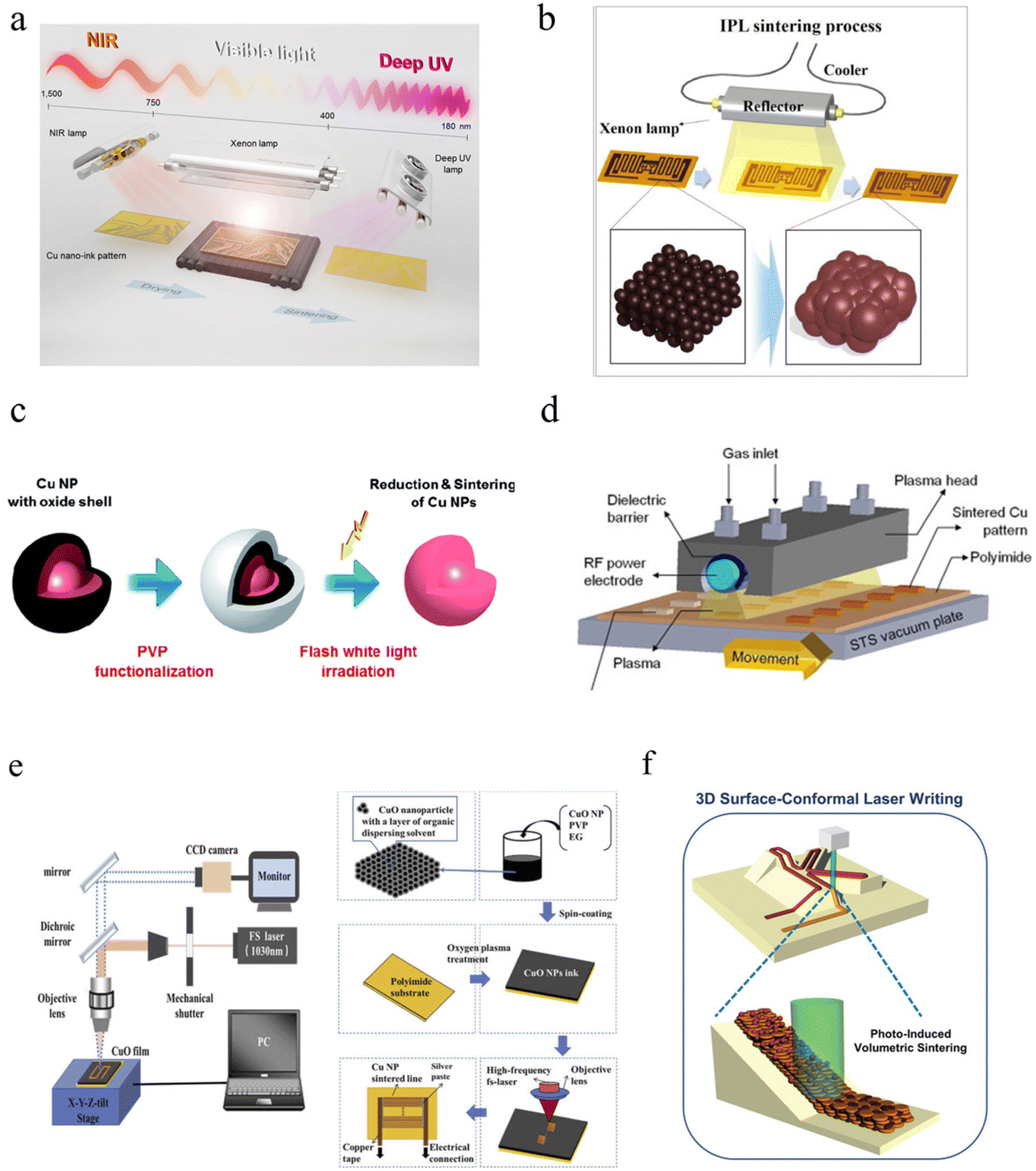 | ||
| Fig. 7 Sintering methods for Cu inks. (a) Schematic of photonic drying and sintering of Cu ink.236 Reproduced with permission from ref. 236. Copyright 2016 Springer. (b) Schematic image of IPL sintering.126 Reproduced with permission from ref. 126. Copyright 2020 Elsevier. (c) Schematic of reactive sintering using IPL.237 Reproduced with permission from ref. 237. Copyright 2017 Royal Society of Chemistry. (d) Schematic diagram of atmospheric-pressure plasma sintering system.238 Reproduced with permission from ref. 238. Copyright 2013 Elsevier. (e) Schematic of laser and experiment flow for fabrication of a flexible circuit.185 Reproduced with permission from ref. 185. Copyright 2021 Optical Society of America. (f) Schematic image of the 3D surface-conformal laser writing process for fabricating a copper circuit.239 Reproduced with permission from ref. 239. Copyright 2020 John Wiley and Sons. | ||
4. Antioxidant method
Owing to its atomic structure, copper can easily react with water and oxygen to produce oxides (CuO, Cu2O) under ambient conditions.267 Especially when the size is reduced to the nanometer level, the higher specific surface area will make copper more susceptible to oxidation, which will seriously hinder electron transfer and increase the resistance of the printed film. In addition, high melting point oxides (CuO ∼1446 °C, Cu2O ∼1235 °C) can lead to holes and cracks inside the film during sintering, making the film highly porous and mechanically tough, which limits the application of printed copper inks in electronics.45,142 Therefore, it is crucial to improve the stability of copper nanoparticles under environmental conditions by introducing additional fillers and processes. Depending on the principle, there are two types: chemical and physical treatment.4.1. Chemical treatment
Chemical protection usually uses a solvent to produce a protective layer or remove oxides from the copper. The most mainstream method is to produce a dense passivation layer consisting of metal salts on the outermost surface by reacting an organic corrosion inhibitor with the copper.112,268,269 The passivation layer keeps O molecules from the environment and the electrochemical process of the doped material in the passivation layer can give the passivation layer resistance to acids and alkali. The commonly used corrosion inhibitors are azole nitrogen, amines and some self-assembled organic short chains.270,271 Polat Genlik et al. used benzotriazole (BTA) to passivate the CuNW network. Surprisingly, they found that the sheet resistance of the BTA-passivated film increased by only 1 Ω sq−1 and the transmission decreased by only 2%.168 After bonding with a PEDOT:PSS (pH < 4) layer, the transparent conductive film was not oxidized after heating at 150 °C, which allows the stable presence of CuNW flexible transparent electrodes during the preparation of optoelectronic devices. BTA can form a thin polymer layer that is insoluble in water and organic solvents on the surface of CuNWs, preventing the contact of Cu with O2 and H2O. Considering the toxicity of BTA, Zhou et al. investigated the passivation effect of 1,2,4-triazole with TT-LYK on the copper surface,272 as shown in Fig. 8a. Both corrosion inhibitors can form coordination effects with copper surfaces to produce copper salts, and their reaction equations are shown below:| Cu2+ + 1,2,4-triazole → Cu-1,2,4-triazole |
| Cu2+ + TT-LYK → Cu-TT-LYK |
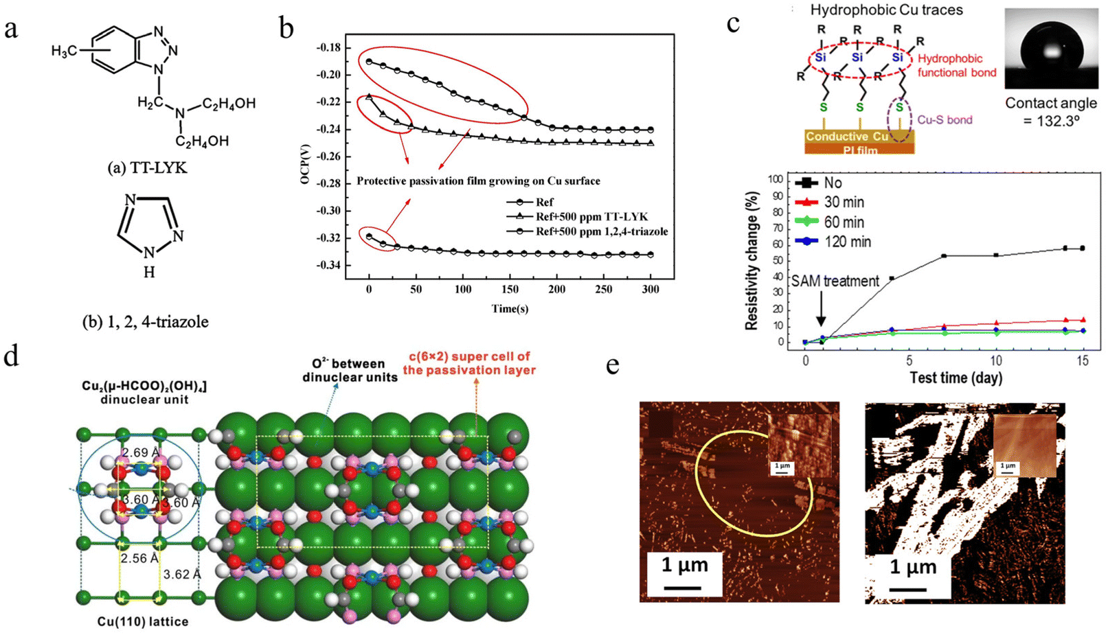 | ||
| Fig. 8 Chemical protection processes. (a) Molecular formulas of TT-LYK and 1,2,4-triazole.272 (b) Change in open circuit potential value for 1,2,4-triazole, TT-LYK, and H2O2.272 Reproduced with permission from ref. 272. Copyright 2020 Elsevier. (c) Schematic of MPTS-passivated copper to improve hydrophobic contact angle and long-term stability.191 Reproduced with permission from ref. 191. Copyright 2018 American Chemical Society. (d) Structure models of the paddle-wheel dinuclear Cu(II) formate complex and the Cu (110) surface.274 Reproduced with permission from ref. 274. Copyright 2020 Springer. (e) Current mapping image for (left) after aging in the oven and (right) after retreatment with acetic acid.167 Reproduced with permission from ref. 167. Copyright 2020 Elsevier. | ||
Using Freundlich adsorption isotherm fitting, the standard adsorption free energies of 1,2,4-triazole and TT-LYK were −25.92 kJ mol−1 and −23.43 kJ mol−1 (between −20 and 40 kJ mol−1), respectively, indicating that these two corrosion inhibitors formed multiple passivation layers on the copper surface, mainly by physical adsorption and supplemented by chemical adsorption (Fig. 8b). The similarity of the two corrosion inhibitors in the adsorption type and passivation process allowed the mixture to improve the corrosion inhibition of the films further. Kwon et al. used 3-mercaptopropyl-trimethoxysilane (MPTS) to passivate the sintered copper films based on the strong covalent bonding between Cu and S.191 The weak Cu(II) and Cu(I) elements present in the copper films were effectively removed to obtain the metal salt of Cu(SC3H6Si(OCH3)3). This passivation layer protects the copper from resistance setting under ambient conditions for 15 days, as shown in Fig. 8c.
Self-assembled organic short chains play a prominent role in passivating copper without affecting the electrical conductivity. Recently, Peng et al. investigated the effect of passivating copper with sodium formate on oxidation resistance and corrosion without affecting electrical conductivity.273 They found that the formate treatment leads to a (110) lattice reconstruction on the surface of copper foil. The four OH− on the double-core Cu2(μ-HCOO)2(OH)4 match perfectly with the outermost Cu(II) to form a Cu(II) → Cu(I) → Cu(0) longitudinal structure. This dense passivation structure hinders the adsorption of oxygen and water on the copper surface and shows a good anticorrosion effect under the action of NaOH, salt spray, H2O2, and Na2S, while the reason for not affecting the electrical conductivity may be the quantum tunneling effect. However, it should be noted that the formic acid passivation layer cannot exist under strongly acidic conditions, so the passivation process should avoid pH < 3. Based on the excellent effect of formate, Sheng et al. used iodine ions to control copper growth to obtain 2D morphological Cu nanoplates with (111) surface as the base.97 The Cu nanoplates immersed in formate solution formed a dense passivation layer covered by formate on the Cu (111) surface after 12 h treatment at 120 °C. The passivated Cu-FA showed good stability at 350 °C and the resistance increased by only 10% after one day of immersion in 0.1 M NaOH solution (Fig. 8d). The formate decomposition temperature is low, with few by-product residues and good passivation protection, but the current studies all require a long treatment time (about 12 hours) in an formate solution environment to obtain good passivation.
In addition, the use of acidic solutions (lactic acid, acetic acid, formic acid) also plays a role in improving the electrical conductivity.173,265,275 The reason is that acids can remove oxides from the surface of copper particles through reduction reactions, and most organic capping agents (such as HDA and ODA) are more soluble in acidic solvents. Therefore, acids can be used to remove oxide and organic residues during the deposition of CuNWs for transparent conductive films. Hashimi et al. prepared transparent films of CuNWs with a sheet resistance of 35 Ω sq−1 and 81% transmittance using an optimized purification method.167 Owing to the oxidation problem of copper nanowires with a high aspect ratio, the sheet resistance initially increased 10 times. However, the sheet resistance of the film can be significantly reduced to the initial value by acetic acid immersion for 10 min, and this phenomenon can be repeated up to five times. Acid solvent immersion treatment is simple and fast, but can cause environmental pollution problems, while an excessive number of rinses will reduce the initial conductivity of copper printed films, which is caused by the peeling of copper particles from the surface during the cleaning process (Fig. 8e).
4.2. Physical treatment
Physical protection also involves applying a protective layer, but the difference is that no chemical reaction is involved in the formation of copper salts. Depending on the degree of encapsulation, physical protection can be divided into core–shell and coating structures.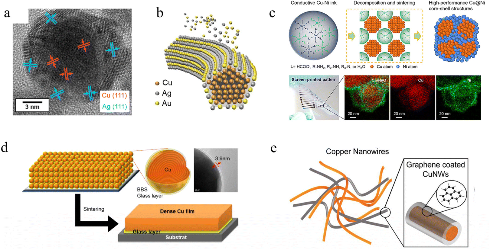 | ||
| Fig. 9 The core–shell structure. (a) HRTEM image of a Cu@Ag nanoparticle.119 (b) Schematic illustration of CuNW@alloy core–shell structure.61 Reproduced with permission from ref. 61. Copyright 2020 Elsevier. (c) Flow chart of fabrication Cu@Ni nanoparticles by co-reduction and EDS element analysis.127 Reproduced with permission from ref. 127. Copyright 2022 American Chemical Society. (d) Schematic image of Cu@BBS nanoparticles and the sintering for dense Cu film.277 Reproduced with permission from ref. 277. Copyright 2021 Elsevier. (e) Schematic illustration of Cu@graphene by thermal decomposition of dopamine.217 Reproduced with permission from ref. 217. Copyright 2021 American Chemical Society. | ||
Although galvanic displacement is the simplest method without additional reducing agents and additives, the reaction consumes copper particles, resulting in surface defects, which is not suitable for preparing CuNWs with core–shell structures. This will reduce electrical conductivity, because the reduction in diameter significantly affects the electron transport, especially when the linewidth is close to the mean free range of the electrons. Stewart et al. found that the core–shell copper nanowires with good structure can be obtained by using chemical deposition.278 The addition of ascorbic acid in alkaline solution inhibits the oxides and promotes the reduction of silver ions on the surface of CuNWs, leading to Cu@Ag nanowires that were stable at 160 °C and 85% RH for 24 hours. Zhang et al. formed a homogeneous alloy protective shell by co-depositing Au and Ag atoms in KAu(CN)2 and KAg(CN)2 solutions using CuNWs flexible transparent films as the cathode and graphite flakes as the anode,61 as shown in Fig. 9b. The cyanide of Ag and Au can reduce the standard electrode potential difference from 0.7 V (Ag ∼0.8 V, Au ∼1.5 V) to 0.2 V, which achieves good co-deposition for excellent optoelectronic properties (14.2 Ω sq−1 at 90.1% transmission, 2000 times bending) and corrosion resistance (168 h in atmosphere, 200 s in H2O2 solution, 1800 s in sulfuric acid solution to maintain integrity). However, it is noted that the CuNWs must be immersed in the solution after the current is applied, otherwise the galvanic displacement will occur first.
The preparation of a self-assembled core–shell structure by co-reduction of various metal precursors can improve the storage and printing stability of ink. Li et al. reported that a simple mixture of Cu formate and Ni formate composite inks can spontaneously form Cu@Ni core–shell nanostructures after thermal annealing at 170 °C for 15 min.127 Different decomposition temperatures of copper formate (starting at 110 °C) and nickel formate (starting at 185 °C) were found to be critical for the generation of core–shell structures by thermogravimetry-differential thermal analysis coupled with mass spectrometry (TG-DTA-MS). Moreover, the catalytic effect of copper reduced the overall decomposition temperature (∼170 °C). Depending on the Ni content, the printed patterns have a high electrical conductivity of 19–67 μΩ cm and high oxidation resistance at 180 °C ambient conditions.
Cu-shell structures can also be prepared by using inorganic compounds or carbon materials. Tigan et al. used atomic layer deposition (ALD) to prepare CuNWs@Al2O3/ZnO.276 Compared with conventional bare CuNWs transparent film heaters (∼100 °C), the shell layer protection allowed the upper heating limits to be raised to 273 °C and 204 °C with uniform heating. Xiao et al. used microwave-induced metal dissolution to synthesize CuNWs@ZnS, and the visible light response due to the narrowing of the band gap enabled the H2 evolution rate to reach 10722 μmol h−1 g and the quantum efficiency to reach 69% under 420 nm LED light irradiation.63 Jung et al. used ultrasonic spray pyrolysis to achieve large-scale preparation of Cu@barium borosilicate (BBS) glass particles.277 The melting point difference between metallic copper and BBS glass formed a core–shell structure with a shell layer only 3.9 nm thick. The sintering process with BBS glass as binder and accelerator achieved good adhesion of copper to the substrate and high-density patterning with a film resistivity of 2.01 μΩ cm (very close to the resistivity of pure copper), which only increased to 2.26 μΩ cm after one month exposure to air. The excellent electrical and thermal conductivity of graphene mean that it can also be used as a shell layer material. Dopamine stirred in copper ink can decompose at high temperatures to produce graphene shell layers in situ, but annealing temperatures above 800 °C are only applicable to highly temperature-resistant substrates, such as ceramics.150,217
Considering the oxidation problem of water molecules from microcracks and pinhole leakage of PI, Hong et al. spin-coated PI resin on prepared copper nanowire films and deposited a 100 nm thick SiOx layer on the PI layer as a sealing layer,279 as shown in Fig. 10a. The comparison revealed that CuNWs with the SiOx sealing layer showed almost no change in heating resistance at high temperature over 320 °C and also had electrical properties comparable to those of AgNWs after 7 days under a humid environment. However, this method introduces an additional process of depositing the coating. Organic coatings can be electropolymerized on copper surfaces by voltammetric cycling in acidic solutions. Ma et al. electropolymerized PANi, PNEA, and molybdate-doped PANi-Mo and PNEA-Mo coatings on copper surfaces in oxalic acid solutions.280 The XPS and molecular dynamics analysis revealed that the introduction of the ethyl group in the organic polymer backbone reduces the physical defects of the coating, and the molybdate doping further reduces the porosity of the coating and repel the cations in the solution to maintain the charge balance inside the coating, as shown in Fig. 10b.
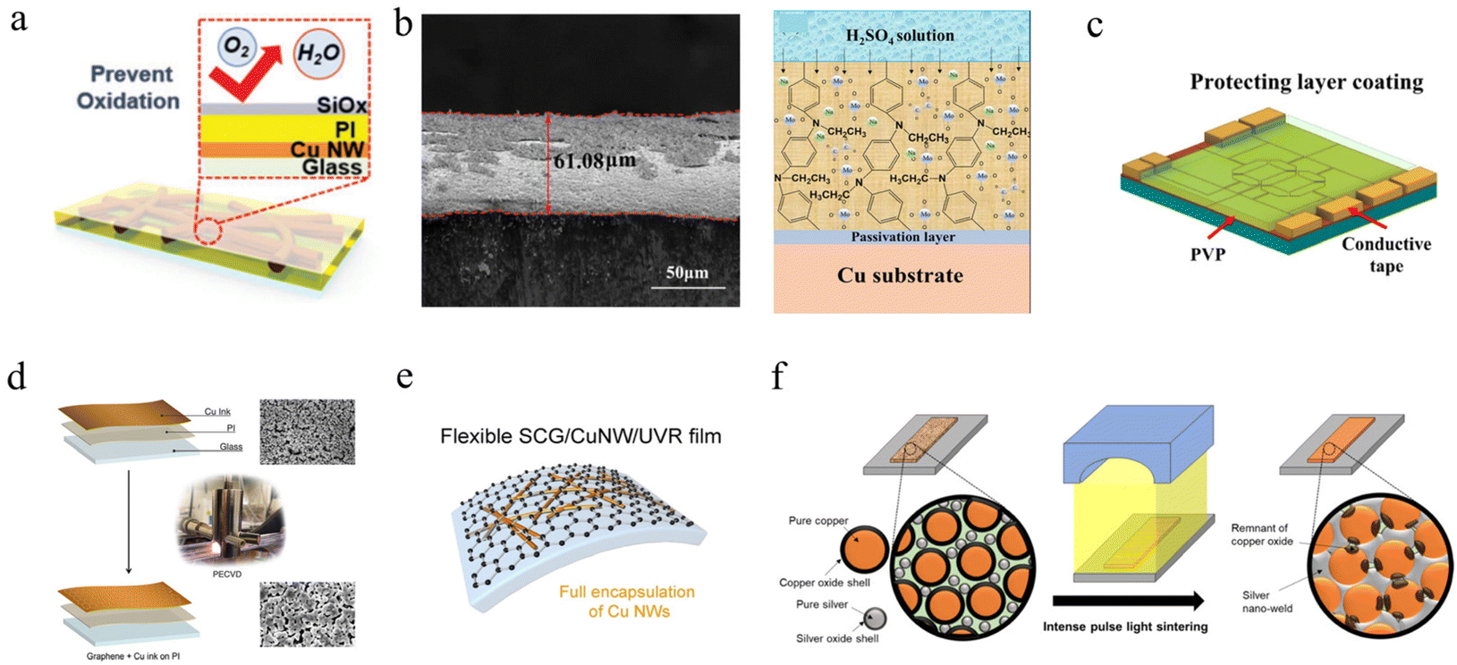 | ||
| Fig. 10 Coating structure. (a) Schematic illustration of CuNWs/PI/SiOx composite film.279 Reproduced with permission from ref. 279. Copyright 2019 John Wiley and Sons. (b) Cross-section SEM of PNEA-Mo coating and schematic of the anticorrosion mechanism of PNEA-Mo coating in H2SO4 solution.280 Reproduced with permission from ref. 280. Copyright 2020 Elsevier. (c) Schematic diagram of coating a PVP layer onto a Cu electrode.169 Reproduced with permission from ref. 169. Copyright 2020 Elsevier. (d) Schematic of coating graphene on Cu film by PECVD.113 Reproduced with permission from ref. 113. Copyright 2021 American Chemical Society. (e) Schematic of the flexible SCG/CuNWs/UVR composite film.170 Reproduced with permission from ref. 170. Copyright 2020 Elsevier. (f) Schematic of the welding process by AgNPs via IPL.121 Reproduced with permission from ref. 121. Copyright 2021 American Chemical Society. | ||
The excellent electrical conductivity, light transmission, and high sealing properties of graphene make it ideal as a coating material. Lu et al. used the plasma enhanced chemical deposition (PECVD) process to deposit graphene on copper ink to achieve copper ink reduction, sintering, and passivation in one step.113 Conductive copper patterns with a resistivity of 0.03762 mΩ cm were produced at an optimal ratio of H2/CH4 = 8. This rapid preparation using the integrated coating and sintering process is favorable for large-scale copper ink applications. However, problems such as steps and defects at the polycrystalline copper interface affect the graphene adhesion stability, and defects such as voids and folds after polycrystalline graphene adhesion do not effectively prevent the contact of corrosive elements (O2, H2O) with copper. Wang et al. prepared transparent conductive films with a UV-curable resin–CuNWs–monocrystalline graphene structure.170 CVD was used to deposit a single monocrystalline graphene layer on copper (111) foil. The perfect interface of Cu (111) allows the single-crystal graphene to be seamlessly stitched together to form a continuous network, giving the CuNWs transparent conducting network excellent electrical properties (19 Ω sq−1, 84.3% transmittance) and oxidation resistance (ΔR/R0 < 0.2 after 180 days under ambient conditions). However, controlling the growth of this graphene and additional wet etching of the copper foil increases the cost of using this process, which is still a challenge in applying to industrial production.
In addition, metal fillers as coating materials can also effectively improve the durability of copper inks, which is related to the copper particle sintering process.120,121,123 Sintering drives the movement of the outer atoms of copper and the nearby atoms to combine to form a neck connection. Owing to the smaller diameter and increased contact area, the Cu neck connection is usually fragile. The additional metal filler acts as a bridging agent for the independent copper source during the sintering process, reducing the disadvantages of easy oxidation and poor mechanical toughness caused by the copper neck connection. The commonly used metal fillers are Ni, Sn, and Ag due to their lower melting points and better stability than Cu. Chen et al. developed a Cu/Sn hybrid ink. The low melting point of Sn allowed for a 21% reduction in the energy required for IPL sintering while achieving good connectivity around the Cu nanoparticles (14 Ω sq−1).131 Cu/Sn inks achieved better adhesion after sintering compared to pure Cu inks and were almost defect-free when prepared at ultrafine line widths (3.5 μm). Chung et al. used electro-explosion to prepare Cu/Ag hybrid nanoparticles (4.06 μΩ cm) on PI substrates under optimized voltage conditions and flash sintering light energy, and the conductive patterns were able to exist stably for more than 15 h when heated at 100 °C.133
5. Applications
The remarkable electrical properties of copper-based inks have motivated their applications for electronic components, such as flexible transparent heaters (FTHs),96,276,279 transparent conductive electrodes (TCEs),158,281 sensors,217,266 thin-film transistors,93,117 photovoltaic devices147,170 and antennas.65,125 Here, we will briefly summarize the recent progress in the development of copper-based functional electronics.5.1. Transparent conductive electrodes (TCEs) and flexible transparent heaters (FTHs)
Conventionally used transparent electrodes of ITO have disadvantages such as high price, rigidity, and preparation requirements. CuNWs have become the most promising alternative to ITO in achieving high conductivity and high transmission owing to the high aspect ratio.158,160,276 Although CuNWs are non-transparent, the high aspect ratio allows them to achieve lateral conductivity with a low duty cycle. The quality of the sample can be measured by the sheet resistance (Rs) and the transmittance (Tg) under 550 nm wavelength. The figure of merit (FoM) is defined as:282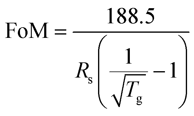
The FoM values calculated for some TCEs are compiled in Table 2. Tran et al. used a nanosecond pulsed laser to sinter CuNWs for the selective preparation of high-performance TCEs.169 The laser energy density and scanning speed were optimized by simulation to eliminate thermal damage to the flexible substrate, and the obtained CuNWs TCEs had a sheet resistance of 60 Ω sq−1 and a transmittance of 93.6% at 550 nm. Acetic acid immersion removes impurities such as copper oxide and PVP, resulting in a 5% increase in the resistance of the transparent electrode at 1500 cycles with a 10 mm bend radius. Zhong et al. prepared large-scale CuNWs TCE (22.1 Ω sq−1, 85.6% transmittance), IPL irradiation of CuNWs self-embedded in plastic substrates provided excellent mechanical toughness (10000 cycles of bending durability and over 120 hours of resistance stability under ambient conditions) so that the LEDs can stably illuminate even under bending and pasting,160 as shown in Fig. 11a. Alternatively, TCEs can be prepared by artificially controlling the duty cycle of copper traces to achieve a mesh structure.131 Kwon et al. prepared a conductive copper network with a line width of 20 μm and a blank width greater than 200 μm using selective laser sintering of CuNPs ink coated on PEN.283 The conductivity of the copper pattern was 1.67 × 10⁻⁴ Ω m, and at a bending radius of 2.25 mm it could be continuously cycled 1000 times, as shown in Fig. 11b.
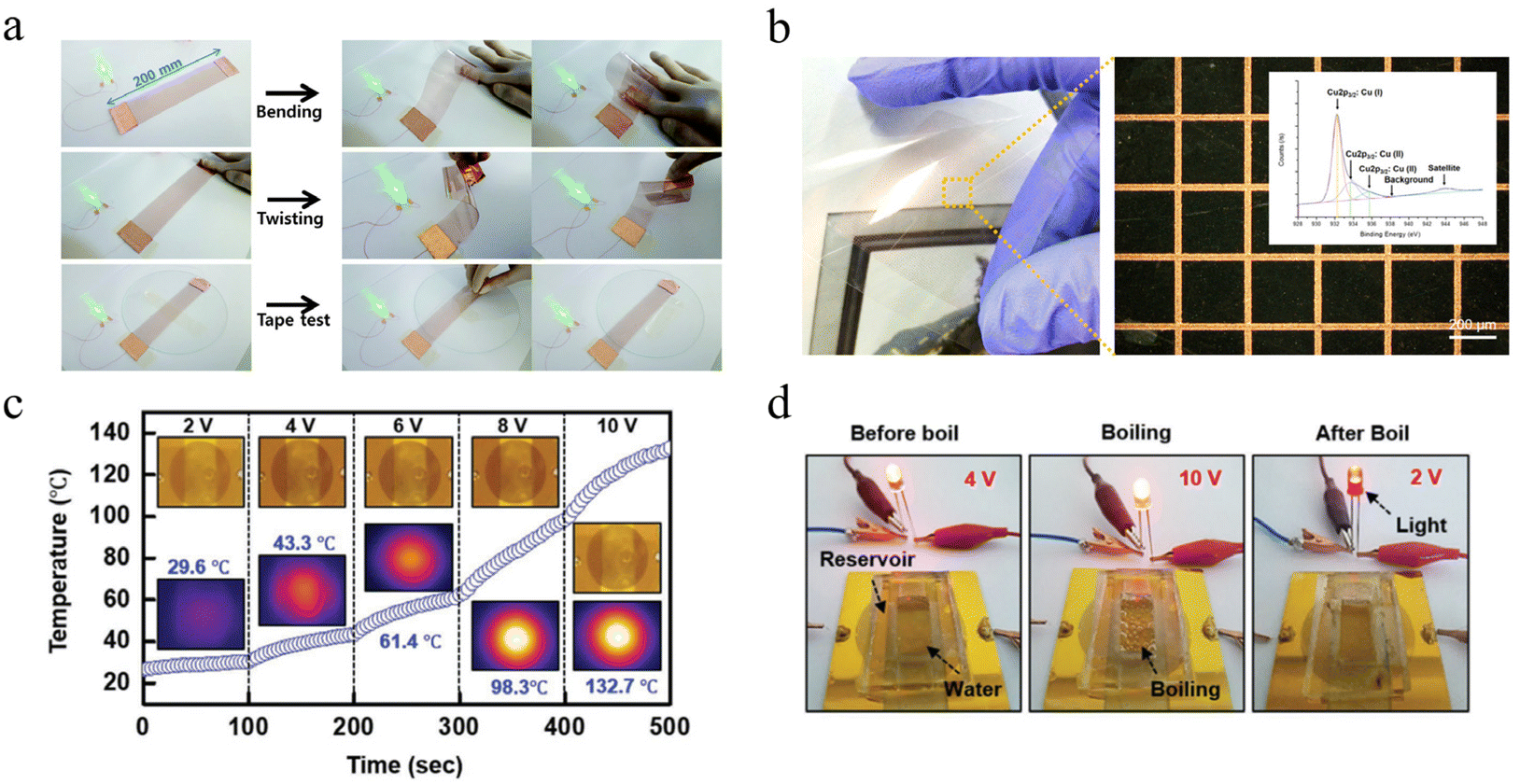 | ||
| Fig. 11 (a) Photographs of the LED circuit with TCE.160 Reproduced with permission from ref. 160. Copyright 2016 Royal Society of Chemistry. (b) Optical image of Cu grid transparent conductor.283 Reproduced with permission from ref. 283. Copyright 2016 American Chemical Society. (c) Time-dependent temperature curves of FTH by applying voltage.279 (d) Photographs of water boiling before and after being heated by FTH.279 Reproduced with permission from ref. 279. Copyright 2019 John Wiley and Sons. | ||
Due to the resistance Joule effect Q = V2 × t/R, transparent heaters can be used for defrosting and de-icing displays and composite glass for LCDs, billboards, and vehicles.96,276 Hong et al. prepared CuNWs transparent conductive film with water and oxygen barrier (relative resistance change less than 0.3 times after 7 weeks of immersion in water).279 A uniform heating case of 132.7 °C can be obtained at 10 V. Even if the PDMS mill is filled with water above, it can be heated to boil water without affecting the light intensity change of the series LED lamps, as shown in Fig. 11c and d. Zhong et al. prepared FTHs heaters using a roll-to-roll process combined with IPL irradiation; the temperature distribution was uniform under the applied voltage, and the temperature rise with the voltage rise would reach saturation within 70 s.212 Bobinger et al. prepared FTHs (Rs = 10.3 Ω sq−1, T = 83.4%) by inkjet using copper chloride as a precursor for the preparation of CuNWs.164 The FTHs were able to be heated uniformly and the resistance remained well linear with temperature. Subsequently, they prepared a heating film using a similar copper nanowire system and applied it to a thermoacoustic loudspeaker for the first time (the response was in good agreement with the simulation fit).165 Although the copper FTHs can obtain a good heating effect and fast response time, copper is easily oxidized at high temperatures, leading to a severe decrease in its electrical conductivity.
5.2. Sensors
Copper ink applied by printing techniques can be directly used as a flexible sensor to detect physiological and physical signals, which can be used for the expensive metal sensing components in commercial applications.64,150,155,168,191 The excellent mechanical toughness of CuNWs is widely used in the field of strain sensors. Zhang et al. prepared CuNWs@IOnGel composite films with porous structure using PS microspheres.266 The porous structure created by the PS microspheres within the gel improves the compressibility of the film and exhibits extremely high sensitivity as a pressure sensor (S = 39.7 kPa−1 in the range of 0.7–1000 Pa). The embedded structure of nanowires and gels provides the sensor with good mechanical stability (3000 finger bending cycles). They demonstrated the composite film as a sensor to monitor human physiological signals, effectively identifying three TCM static pulse waves (Chen, Zhong, and Fu), as shown in Fig. 12a. Khuje et al. prepared CuNWs pressure sensors on piezoelectric ceramics.217 The array of sensors was attached to the surface of human skin to monitor small pulse signals. The sensing mechanism can be explained by the fact that the longitudinal pressure forces the presence of more CuNWs contact points at the upper and lower interfaces, providing more channels for electron transport and leading to a decrease in film resistance, as shown in Fig. 12b and c. Kwon et al. inkjet-printed copper inks with high adhesion on PI substrates.191 It has high oxidation resistance (stable under ambient conditions for more than 15 days) while maintaining ultra-high mechanical durability (100000 bending cycles). In the absence of conductive gel, the copper electrodes are capable of stable measurement of ECG, EMG and EOG signals. Wearable electronic devices also need to work stably for the long-term. Zhang et al. showed highly conductive (0.808 Ω sq−1) and flexible (1000 bending cycles) composite films obtained using reduced graphene oxide (RGO) and CuNWs.284 By depositing on polyester cloth, the thin and light flexible circuits can be used for LED lighting for long periods of time (>30 days under ambient conditions).
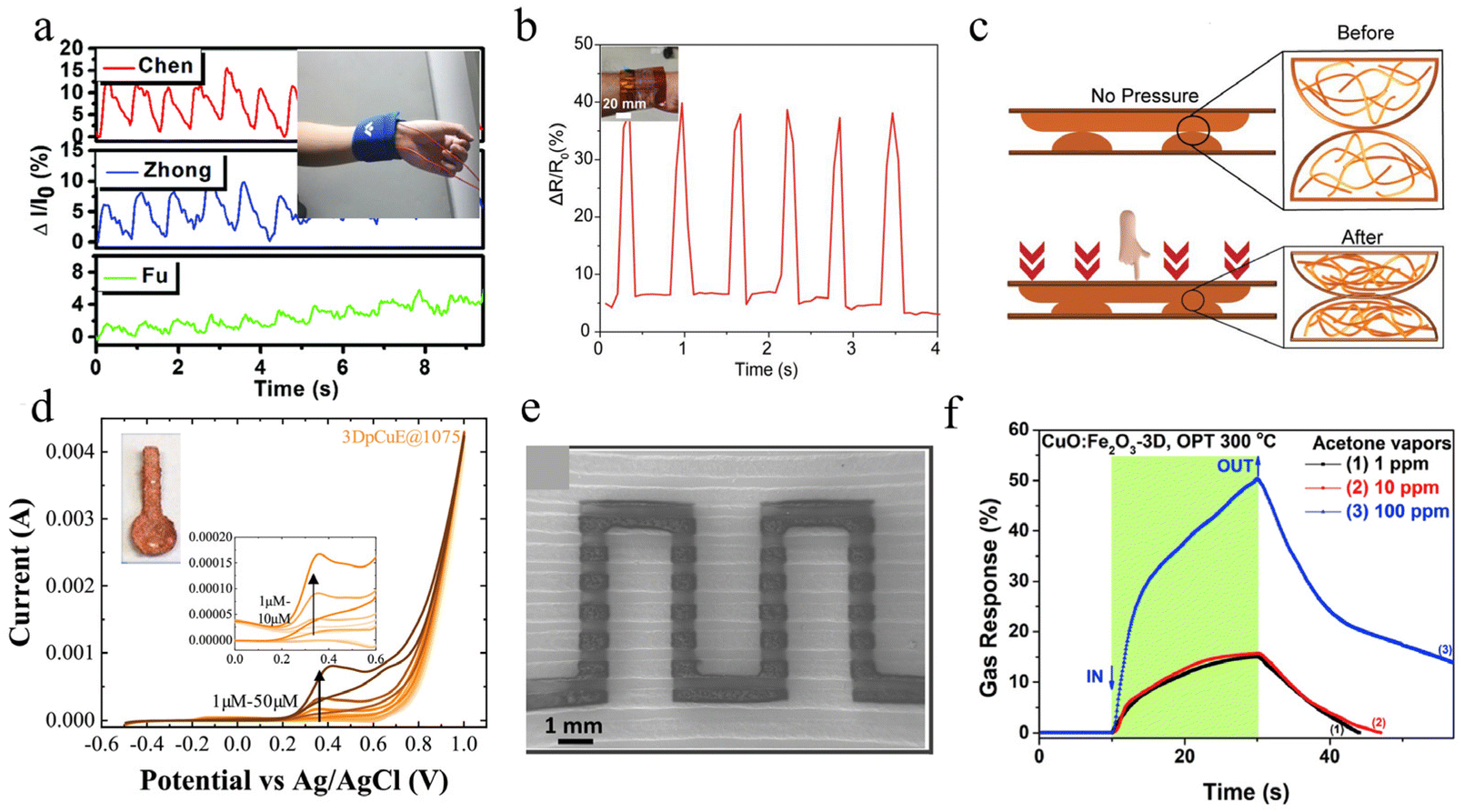 | ||
| Fig. 12 (a) Three different test pressures by TCM are defined. Inset: Photograph of tester's pulse test.266 Reproduced with permission from ref. 266. Copyright 2020 Royal Society of Chemistry. (b) Plot depicting the sensor performance for characterizing the arterial pulse. Inset: Photograph of tester's pulse test. (c) The sensing mechanism of the resistive pressure sensor.217 Reproduced with permission from ref. 217. Copyright 2021 American Chemical Society. (d) Cyclic voltammograms of different concentrations of glucose. Inset: Photograph of the sensor.264 Reproduced with permission from ref. 264. Copyright 2020 Elsevier. (e) SEM of acetone sensor.211 (f) Dynamic response at operating temperature of 300 °C to 1, 10 and 100 ppm of acetone vapor.211 Reproduced with permission from ref. 211. Copyright 2020 Elsevier. | ||
The higher sensitivity and lower oxidation potential of copper are also widely used in electrophysiological applications. Redondo et al. demonstrated for the first time the application of 3D-printed pure copper electrodes prepared using fused filament fabrication (FFF) for non-enzymatic sensing of glucose.264 By optimizing the sintering temperature to obtain the highest purity copper film, the sensor exhibited a wider linear range (1–50 μM), lower monitoring limit (0.06 μM), and higher sensitivity (0.03 μM−1 cm−2) compared to other copper-based systems, as shown in Fig. 12d. Siebert et al. mixed micron-sized copper and iron powders through 3D printing to form a continuous pattern, thermally annealed in the air to form a heterojunction structure of metal oxides.211 Based on the physicochemical changes occurring at different temperatures, the sensor has good selectivity for acetone vapor at an operating temperature of 300 °C with a gas response of 50% at 100 ppm vapor concentration and a minimum power consumption of 0.26 μw, as shown in Fig. 12e and f. The excellent performance is attributed to the metal oxide pinpoint contact porous bridging structure.
5.3. Optoelectronic devices
In order to prepare flexible optoelectronic devices, flexible conductive electrodes must first be prepared. Copper ink can be printed on a variety of flexible substrates (PET, PEN, PES) to give the traditional rigid electrodes bendable and foldable characteristics, and its low cost and high conductivity mean it is the main material to replace precious metal (Ag, Au) electrodes,28,29 as shown in Fig. 13. Yang et al. developed a bottom electrode for a flexible perovskite solar cell (PSC) by depositing a protective layer of ZnO with Al doping (AZO) on the CuNWs transparent conducting electrode using atomic layer deposition (ALD).171 While retaining excellent electrical properties (34.05 Ω sq−1, 87.77% transmittance at 550 nm), the protective layer of AZO also effectively prevents the diffusion of iodine ions from perovskite into the CuNWs electrode to induce the decomposition of NWs (almost no change in resistance after 7 days of exposure to the perovskite layer). The power conversion efficiency (PCE) of the PSCs prepared based on this composite electrode was 14.18% and the filling factor (FF) was 70.77% by improving the energy band arrangement in the interfacial layer. Moreover, the PCE changed non-significantly after 600 cycles at 12.5 mm bending radius. Im et al. first demonstrated flexible OLED devices using CuNW transparent conductive electrodes.147 High-performance fiber-reinforced transparent plastic conductive films (Rs = 25 Ω sq−1, transmission = 82%) were prepared by encapsulating CuNWs with UV light-curable resin. Even after 10000 cycles at a bending radius of 5 mm and 14 days of aging test at 80 °C, there was no significant change in resistance. The prepared windmill-shaped OLEDs achieved a maximum luminance of about 104 cd m−2 at a driving voltage of 9 V with a current density much higher than 102 mA cm−2, and can stably emit green light under bending. Wang et al. prepared flexible OLEDs using a single layer of monocrystalline graphene and UV-curable resin to protect CuNWs for improved durability as an anode output.170 Compact coverage of CuNWs with a single graphene layer results in electrodes with good mechanical durability (>1000 cycles) and long-term stability (<0.2 times change in resistance after 100 days under ambient conditions).
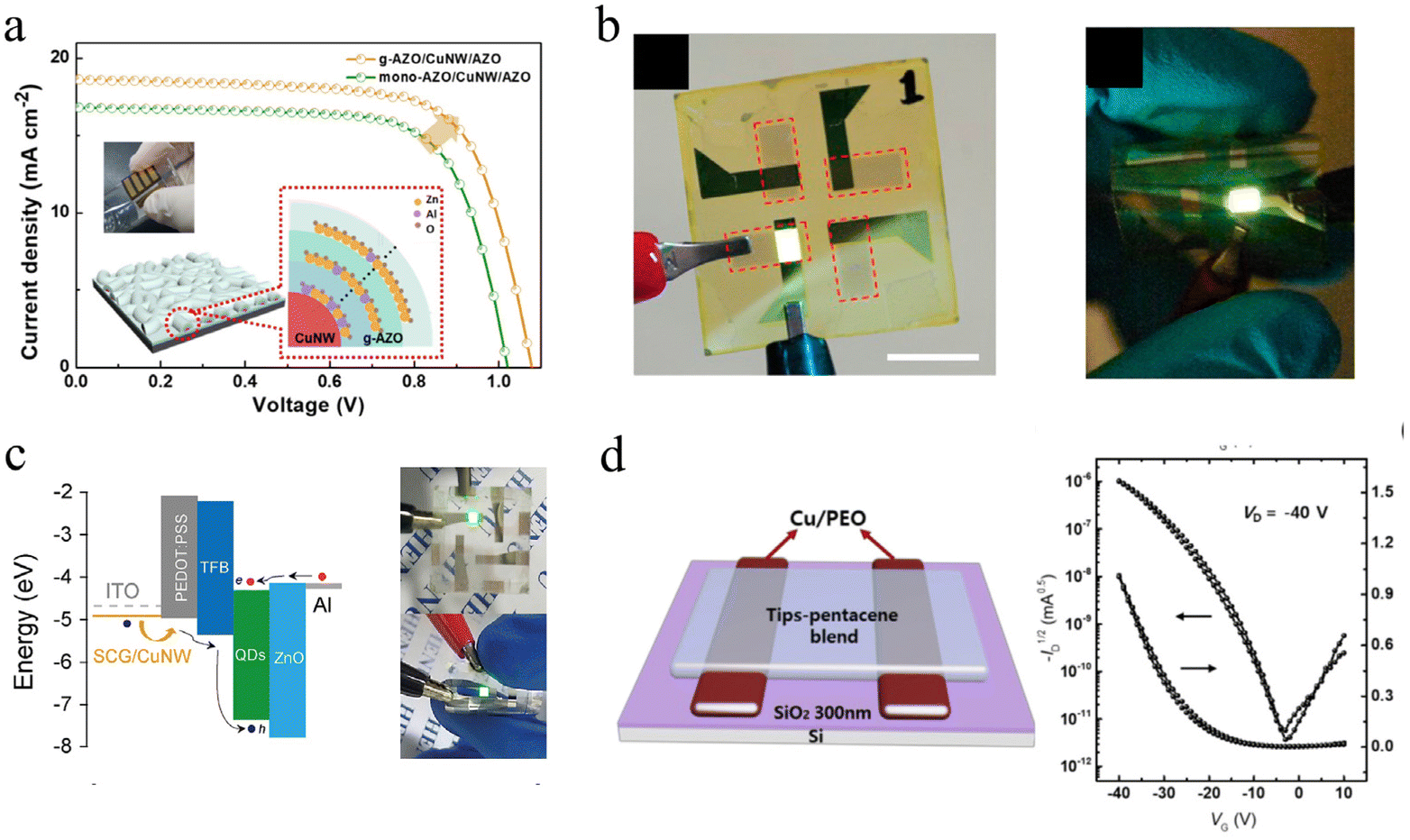 | ||
| Fig. 13 (a) The J–V curves of flexible PSCs based on different electrodes. Inset: Photograph of flexible PSC and schematic diagram of doping Al.171 Reproduced with permission from ref. 171. Copyright 2020 American Chemical Society. (b) Photograph of OLED device operating in (left) flat and (right) flexed states.147 Reproduced with permission from ref. 147. Copyright 2014 American Chemical Society. (c) Energy band diagram of the OLED device (left) and photograph of the OLED operating in different states (right).170 Reproduced with permission from ref. 170. Copyright 2020 Elsevier. (d) Schematic image of the OFETS (left) and transfer characteristics of OFETs (right).285 Reproduced with permission from ref. 285. Copyright 2020 Elsevier. | ||
The composite film has a higher work function (4.87 eV) compared to the ITO (4.7 eV) anode, which increased the hole injection rate and the luminance to 8760 cd m−2 at a current density of 4.25 cd A−1. This is much higher than the OLED with flexible ITO (1.2 cd A−1 at 5883 cd m−2).
Similarly, CuNP inks play an important role in optoelectronic devices. In contrast to the CuNWs thin-film approach, a controlled Cu grid trace is used to replace ITO electrodes. This has the great advantage of reducing the cost of production, knowing that the synthesis of CuNWs is much more complex than CuNPs. Georgiou et al. prepared the first OPVs using CuNPs ink as a substrate electrode by using inkjet-printing.286 The best PCE value of 3.35% was obtained when the number of Cu grids was six (17% c overage, Jsc = 11.39 mA cm−2, FF = 50.72%). However, this Cu electrode oxidizes rapidly at 160 °C in an air environment, leading to device failure, and the exposed Cu electrode will cause large leakage currents owing to the line height and surface roughness. One year later, the same group prepared the first ITO-free OLED based on a CuNPs/PEDOT:PSS hybrid substrate electrode with an improved process.287 Instead of depositing copper ink directly on the substrate, they chose to pre-deposit it on the glass substrate and then transfer it to the substrate by the reverse nanoimprinting transfer method to form embedded Cu grids. The biggest advantage of this approach is that it results in a flatter surface for the electrodes, reducing leakage current and thus increasing efficiency, resulting in a maximum CE of 3.6 cd A−1. In the same way, Kamijo et al. demonstrated high-resolution OLEDs with CuNPs grids as the bottom electrodes.288 The OLED luminescence intensity in the case of CuNPs ink traces with small pitch (<5 μm) and narrow line widths (0.5 μm) was close to that of the ITO reference. Similar to the previous work, a thickly doped hole injection layer is used to reduce the roughness of the Cu gate electrode and avoid short circuits.
5.4. Thin-film transistors
Thin-film transistors are the basic components of smartphones and other electronic displays.289,290 Although there have been many studies on the trench layer, there are disadvantages of complicated processes (magnetron sputtering, vapor deposition) and expensive materials (gold, silver) for the deposition of the source–drain connecting the trench.291,292 Copper can solve the high cost problem owing to its high resistivity and low price, and the transistors obtained by printing can also exhibit properties such as flexibility and stretchability. Can et al. used EHD to print a copper source–drain on ZTO under vacuum sintering (380 °C) for transistors.117 The average effective mobility in the saturation region was 0.50 cm2 V−1 s−1 with an on-to-off current ratio of 5.5 × 10⁵. Li et al. investigated the effect of different ratios of poly(ethylene oxide) on the viscosity of copper nanoplate ink and prepared organic field-effect transistors on SiO2 substrates in combination with IPL sintering.285 The average field-effect mobility was 0.253 cm2 V−1 and the on/off current ratio was 106.5.5. Flexible circuits
Flexibility is the goal of future electronic devices. Lightweight, easy to produce, and reliable complex integrated systems require highly conductive, low-cost interconnection paths.293,294 Copper ink is the most promising material for preparing flexible circuits, which can be achieved by printing on flexible substrates (PET, PEN, PES). Zareei et al. prepared flexible circuit-lit LEDs by screen printing copper–silver hybrid inks on PET.121 The lowest porosity of 1.2% and square resistance of 0.072 Ω sq−1 were obtained with an AgNPs content of 16 wt% and IPL sintering photon energy density of 10.6 J cm−2. This gave the best adhesion to PET substrate without peeling even after pasting by tape, and maintained high conductivity for 7 days even under harsh conditions (70 °C, 100% RH). Chen et al. prepared copper patterns (14.3 μm thickness and 5.68 μΩ cm) on PI substrates by inkjet printing with a two-step chemical plating process.189 The Cu pattern printed on the PI substrate has smooth edges, exhibits a distinct metallic luster, and can be bent many times. Even after one year of operation, the LEDs continue to light up, as shown in Fig. 14a. Son et al. prepared flexible circuits (2.1 × 10⁻⁷ Ω m and 100 μm line width) using copper nanoparticle inks protected by 1-octanethiol coating.95 The circuit is stable under environmental conditions for 2 months and can withstand 1000 cycles of bending tests. Good electrical conductivity was achieved by stable lighting of the LEDs even after bending, as shown in Fig. 14d. Stretchable copper electrodes have been reported. Han et al. prepared highly flexible conductors using laser-welded CuNWs on Eco-Flex films under ambient conditions.252 The conductive films obtained by this method were able to maintain a stable resistance at 250% stretching and for 20000 bending cycles compared to conventional thermal annealing, which causes warping and rupture of the films, as shown in Fig. 14b. Won et al. prepared spiral PDMS mills by casting and then transferred CuNWs to the mills to obtain stretchable conductors with a special structure,163 as shown in Fig. 14c. The relative resistance of this conductive spring changed by only 3.9% at 700% stretching.
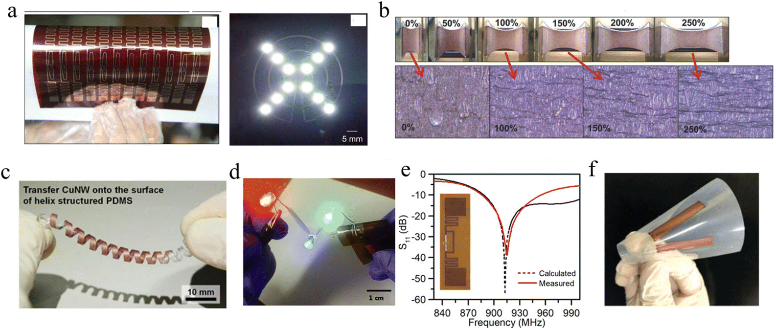 | ||
| Fig. 14 (a) Photograph of flexible Cu pattern on PI substrate (left) and operation of LED chips connected to conductive Cu patterns.189 Reproduced with permission from ref. 189. Copyright 2017 Elsevier. (b) Stretchability test of the CuNWs conductor.252 Reproduced with permission from ref. 252. Copyright 2014 John Wiley and Sons. (c) Photograph of the helical-structured CuNWs electrodes.163 Reproduced with permission from ref. 163. Copyright 2014 Springer. (d) The printed Cu ink on the PI substrate lights the LED under bending conditions.95 Reproduced with permission from ref. 95. Copyright 2018 Elsevier. (e) Calculated and measured S11 results of the fabricated UHF dipole tag antennas. Inset: Photograph of the UHF dipole RFID tag.112 Reproduced with permission from ref. 112. Copyright 2022 Springer. (f) Photograph of Cu V-shaped dipole antenna.125 Reproduced with permission from ref. 125. Copyright 2019 John Wiley and Sons. | ||
5.6. Antenna RF tags
Copper inks are also widely used in flexible antennas and radio frequency identification (RFID) tags.65,66,114,127,238 Hong et al. used formate and thiol-passivated copper paste (with a conductivity of 13400 S cm−1) to fabricate an ultra-high-frequency (UHF) RFID tag by screen printing. The resistance of the passivated copper electrode was stable at 60 °C for more than 500 hours and the dipole antenna has a maximum gain of −2 dB, a reflection coefficient (S11) of −38 dB, and good applicability on PI, paper, and fabric substrates (read ranges of 12.8, 11.3, and 7.7 m, respectively);112 the S11 of RFID is shown in Fig. 14e. Zhang et al. used a composite ink system comprising copper nanowires and copper precursor sintered at low temperature (140 °C) to obtain conductive patterns with resistivity of 14.9 μΩ cm. V-Shaped dipole antennas (length = 30 mm, width = 5 mm, and angle of 30°) were printed on PET, and the antenna return loss was tested at 2.3 GHz at about 32 dB.125
6. Summary and outlook
Copper inks are widely used in the field of flexible printing, with the advantages of low-cost and good electrical conductivity, and are the best substitute for precious metal inks, such as silver. This paper reviewed the research progress of copper-based inks in flexible electronics in recent years, discussed the process improvement of copper ink preparation, printing, and sintering, summarized the methods to improve the conductivity and durability of copper patterns after film formation, and introduced the emerging applications of copper inks in flexible electronic devices, such as transparent electrodes, sensing, optoelectronic devices, and antennas. Although encouraging progress has been made in the development of copper inks, there are still two major problems in the application of next-generation electronic devices: the feasibility of printing patterns and long-term stability.It is still difficult to achieve effective sintering of copper inks on some thermal substrates (PET, PEN), and regulating the parameters of sintering for different ink systems increases the complexity of the preparation process. Copper precursor inks may be a feasible solution to achieve efficient printing and low-temperature sintering. The ionic form avoids blocking the mesh or nozzle during printing and oxidation during storage, and selecting precursors with low decomposition temperature can avoid damage to the flexible substrate during the sintering process. Photonic sintering is an effective method for large-area preparation owing to its advantages of speed and low cost, but high-energy pulsed light may cause local excess heat, which needs further optimization during operation.
The reliability of copper inks in applications is also a major issue of current research. Additives and the copper content in the ink can affect the porosity, surface defects, and step flatness of the film after sintering. Passivation is a simple method that can be operated on a large scale. The development of formic acid roots promises high oxidation resistance without compromising conductivity. However, the formation of dense passivation layers requires the provision of epitaxial copper boundaries with a tight, flat structure, which prevents passivation from improving in efficiency. The rapidity and compatibility of coating protection mean that it could be a future solution to achieve stable copper use, but the preparation process needs to be optimized to improve the degree of wrapping at the interface between the coating and copper.
In addition, adhesion and resolution are also issues that need to be overcome. The degree of adhesion of the copper ink to the flexible substrate determines whether it can work stably in bending and folding situations. This can be improved by adding cellulose to the ink or pretreating the flexible substrate to improve the bonding with the copper molecules. High resolution is a requirement for the miniaturization of printed electronic devices. EHD jet printing and laser sintering are good choices, but the complexity and high cost of the equipment do not match the advantages of copper, causing it to be difficult to achieve in industrial production.
In general, significant progress has been made in the development of copper-based inks. For printability problems, many new methods have been proposed regarding raw materials and additives to obtain uniformly dispersed and easily stored inks. For conductivity problems, methods such as passivation layers and coatings have been proposed to reduce or avoid the generation of oxides. We investigated the development of various conductive inks in the market and predict that the share of copper inks will gradually equal that of the mature and stable silver inks in the next 10 years, with a 30% share of the total.295 The future development of wearable electronic devices will require not only flexibility but also stretchability. Although CuNWs have made progress in the research of stretchable composite elastomers, Cu nanosheets/micron sheets with lower cost are still far from silver composite elastomers in achieving high stretchability. We hope that future research will propose new solutions for the preparation and printing methods of copper-based inks to achieve a printing system with good stability, cost-effectively with a simple process and low waste production, which can promote the development of copper-based ink in the field of flexible printed and wearable electronics.
Conflicts of interest
There are no conflicts to declare.Acknowledgements
The authors acknowledge support from the National Natural Science Foundation of China (52173192), the National Key Research and Development Program of China (2017YFA0206600), the Science and Technology Innovation Program of Hunan Province (2020RC4004), and the Special Funding for the Construction of Innovative Provinces in Hunan Province (2020GK2024).References
- N. Karim, S. Afroj, D. Leech and A. M. Abdelkader, Oxide Electron., 2021, 21–49 CrossRef CAS.
- J. Perelaer, P. J. Smith, D. Mager, D. Soltman, S. K. Volkman, V. Subramanian, J. G. Korvink and U. S. Schubert, J. Mater. Chem., 2010, 20, 8446–8453 CAS.
- S. Afroj, L. Britnell, T. Hasan, D. V. Andreeva, K. S. Novoselov and N. Karim, Adv. Funct. Mater., 2021, 31, 2107407 CrossRef CAS PubMed.
- S. Xu, Z. Yan, K.-I. Jang, W. Huang, H. Fu, J. Kim, Z. Wei, M. Flavin, J. McCracken and R. Wang, Science, 2015, 347, 154–159 CrossRef CAS PubMed.
- N. Matsuhisa, M. Kaltenbrunner, T. Yokota, H. Jinno, K. Kuribara, T. Sekitani and T. Someya, Nat. Commun., 2015, 6, 1–11 Search PubMed.
- M. Yafia, S. Shukla and H. Najjaran, J. Micromech. Microeng., 2015, 25, 057001 CrossRef.
- C. Cho and Y. Ryuh, Sens. Actuators, A, 2016, 237, 72–80 CrossRef CAS.
- C. D. Dimitrakopoulos and P. R. L. Malenfant, Adv. Mater., 2002, 14, 99–117 CrossRef CAS.
- E. Bacher, S. Jungermann, M. Rojahn, V. Wiederhirn and O. Nuyken, Macromol. Rapid Commun., 2004, 25, 1191–1196 CrossRef CAS.
- S. Magdassi, M. Grouchko and A. Kamyshny, Materials, 2010, 3, 4626–4638 CrossRef CAS PubMed.
- K. Chen, W. Gao, S. Emaminejad, D. Kiriya, H. Ota, H. Y. Y. Nyein, K. Takei and A. Javey, Adv. Mater., 2016, 28, 4397–4414 CrossRef CAS PubMed.
- W. Wu, Nanoscale, 2017, 9, 7342–7372 RSC.
- Q. Huang and Y. Zhu, Adv. Mater. Technol., 2019, 4, 1800546 CrossRef.
- L. Nayak, S. Mohanty, S. K. Nayak and A. Ramadoss, J. Mater. Chem. C, 2019, 7, 8771–8795 RSC.
- N. Karim, F. Sarker, S. Afroj, M. Zhang, P. Potluri and K. S. Novoselov, Adv. Sustainable Syst., 2021, 5, 2000228 CrossRef CAS.
- J. Song and H. Zeng, Angew. Chem., Int. Ed., 2015, 54, 9760–9774 CrossRef CAS PubMed.
- M. L. R. Liman, M. T. Islam and M. M. Hossain, Adv. Electron. Mater., 2021, 2100578 Search PubMed.
- M. R. Islam, S. Afroj, C. Beach, M. H. Islam, C. Parraman, A. Abdelkader, A. J. Casson, K. S. Novoselov and N. Karim, iScience, 2022, 25, 103945 CrossRef CAS PubMed.
- T. Q. Trung and N. E. Lee, Adv. Mater., 2016, 28, 4338–4372 CrossRef CAS PubMed.
- W. Yang and C. Wang, J. Mater. Chem. C, 2016, 4, 7193–7207 RSC.
- D. Zhang, B. Chi, B. Li, Z. Gao, Y. Du, J. Guo and J. Wei, Synth. Met., 2016, 217, 79–86 CrossRef CAS.
- X. Xu, M. Luo, P. He, X. Guo and J. Yang, Appl. Phys. A, 2019, 125, 1–7 CrossRef CAS.
- P. He, J. Cao, H. Ding, C. Liu, J. Neilson, Z. Li, I. A. Kinloch and B. Derby, ACS Appl. Mater. Interfaces, 2019, 11, 32225–32234 CrossRef CAS PubMed.
- X. Xu, Y. Chen, P. He, S. Wang, K. Ling, L. Liu, P. Lei, X. Huang, H. Zhao and J. Cao, Nano Res., 2021, 14, 2875–2883 CrossRef CAS.
- X. Liang, H. Li, J. Dou, Q. Wang, W. He, C. Wang, D. Li, J. M. Lin and Y. Zhang, Adv. Mater., 2020, 32, 2000165 CrossRef CAS PubMed.
- S. Lu, J. Zheng, J. A. Cardenas, N. X. Williams, Y.-C. Lin and A. D. Franklin, ACS Appl. Mater. Interfaces, 2020, 12, 43083–43089 CrossRef CAS PubMed.
- T. Zhong, N. Jin, W. Yuan, C. Zhou, W. Gu and Z. Cui, Materials, 2019, 12, 3036 CrossRef CAS PubMed.
- A. Kamyshny and S. Magdassi, Small, 2014, 10, 3515–3535 CrossRef CAS PubMed.
- A. Kamyshny and S. Magdassi, Chem. Soc. Rev., 2019, 48, 1712–1740 CAS.
- Y. Wang, C. Zhu, R. Pfattner, H. Yan, L. Jin, S. Chen, F. Molina-Lopez, F. Lissel, J. Liu and N. I. Rabiah, Sci. Adv., 2017, 3, e1602076 Search PubMed.
- S. Savagatrup, E. Chan, S. M. Renteria-Garcia, A. D. Printz, A. V. Zaretski, T. F. O'Connor, D. Rodriquez, E. Valle and D. J. Lipomi, Adv. Funct. Mater., 2015, 25, 427–436 CrossRef CAS.
- N. Matsuhisa, D. Inoue, P. Zalar, H. Jin, Y. Matsuba, A. Itoh, T. Yokota, D. Hashizume and T. Someya, Nat. Mater., 2017, 16, 834–840 CrossRef CAS PubMed.
- S. Wünscher, R. Abbel, J. Perelaer and U. S. Schubert, J. Mater. Chem. C, 2014, 2, 10232–10261 RSC.
- C. Jin, W. Liu, Y. Xu, Y. Huang, Y. Nie, X. Shi, G. Zhang, P. He, J. Zhang and H. Cao, Nano Lett., 2022, 22, 3372–3379 CrossRef CAS PubMed.
- M. Senel, M. Dervisevic and N. H. Voelcker, Mater. Lett., 2019, 243, 50–53 CAS.
- K. Sim, Z. Rao, H.-J. Kim, A. Thukral, H. Shim and C. Yu, Sci. Adv., 2019, 5, eaav5749 CrossRef PubMed.
- C. Jin, W. Liu, Y. Huang, Y. Xu, Y. Nie, G. Zhang, P. He, J. Sun and J. Yang, Appl. Phys. Lett., 2022, 120, 233701 CrossRef CAS.
- J. Krantz, M. Richter, S. Spallek, E. Spiecker and C. J. Brabec, Adv. Funct. Mater., 2011, 21, 4784–4787 CrossRef CAS.
- N. Matsuhisa, S. Niu, S. J. K. O'Neill, J. Kang, Y. Ochiai, T. Katsumata, H.-C. Wu, M. Ashizawa, G.-J. N. Wang, D. Zhong, X. Wang, X. Gong, R. Ning, H. Gong, I. You, Y. Zheng, Z. Zhang, J. B. H. Tok, X. Chen and Z. Bao, Nature, 2021, 600, 246–252 CAS.
- M. Hauder, J. Gstöttner, W. Hansch and D. Schmitt-Landsiedel, Appl. Phys. Lett., 2001, 78, 838–840 CrossRef CAS.
- M. Singh and S. Rana, Mater. Today Commun., 2020, 24, 101317 CrossRef CAS.
- D. R. Kumar, K. Woo and J. Moon, Nanoscale, 2015, 7, 17195–17210 Search PubMed.
- K. Ankireddy, T. Druffel, S. Vunnam, G. Filipič, R. Dharmadasa and D. A. Amos, J. Mater. Chem. C, 2017, 5, 11128–11137 RSC.
- S. Zhao, F. Han, J. Li, X. Meng, W. Huang, D. Cao, G. Zhang, R. Sun and C. P. Wong, Small, 2018, 14, 1800047 CrossRef PubMed.
- W. Li, Q. Sun, L. Li, J. Jiu, X.-Y. Liu, M. Kanehara, T. Minari and K. Suganuma, Appl. Mater. Today, 2020, 18, 100451 Search PubMed.
- D. Tomotoshi and H. Kawasaki, Nanomaterials, 2020, 10, 1689 CrossRef CAS PubMed.
- K. Kondo, in Copper Electrodeposition for Nanofabrication of Electronics Devices, Springer, 2014, pp. 177–192 Search PubMed.
- J. Xue, J. Song, Y. Dong, L. Xu, J. Li and H. Zeng, Sci. Bull., 2017, 62, 143–156 CAS.
- S. Ding and Y. Tian, RSC Adv., 2019, 9, 26961–26980 CAS.
- X. Li, Y. Wang, C. Yin and Z. Yin, J. Mater. Chem. C, 2020, 8, 849–872 RSC.
- Y. Wang and Z. Yin, Appl. Sci. Converg. Technol., 2019, 28, 186–193 CrossRef.
- W. Li, Y. Yang, B. Zhang, C. F. Li, J. Jiu and K. Suganuma, Adv. Mater. Interfaces, 2018, 5, 1800798 CrossRef.
- W. Li, L. Li, Y. Gao, D. Hu, C.-F. Li, H. Zhang, J. Jiu, S. Nagao and K. Suganuma, J. Alloys Compd., 2018, 732, 240–247 CrossRef CAS.
- J. Ryu, H.-S. Kim and H. T. Hahn, J. Electron. Mater., 2011, 40, 42–50 CAS.
- K. Woo, D. Kim, J. S. Kim, S. Lim and J. Moon, Langmuir, 2009, 25, 429–433 CrossRef CAS PubMed.
- B. K. Park, D. Kim, S. Jeong, J. Moon and J. S. Kim, Thin Solid Films, 2007, 515, 7706–7711 CrossRef CAS.
- I. Kim, Y. Kim, K. Woo, E.-H. Ryu, K.-Y. Yon, G. Cao and J. Moon, RSC Adv., 2013, 3, 15169–15177 RSC.
- P. E. Laibinis and G. M. Whitesides, J. Am. Chem. Soc., 1992, 114, 9022–9028 CrossRef CAS.
- M. P. Mihajlović and M. M. Antonijević, Int. J. Electrochem. Sci., 2015, 10, 1027–1053 Search PubMed.
- Z. Niu, F. Cui, Y. Yu, N. Becknell, Y. Sun, G. Khanarian, D. Kim, L. Dou, A. Dehestani and K. Schierle-Arndt, J. Am. Chem. Soc., 2017, 139, 7348–7354 CrossRef CAS PubMed.
- H. Zhang, Y. Tian, S. Wang, Y. Huang, J. Wen, C. Hang, Z. Zheng and C. Wang, Chem. Eng. J., 2020, 399, 125075 CAS.
- Z. Zuo, F. He, F. Wang, L. Li and Y. Li, Adv. Mater., 2020, 32, 2004379 CrossRef CAS PubMed.
- S. Xiao, W. Dai, X. Liu, D. Pan, H. Zou, G. Li, G. Zhang, C. Su, D. Zhang and W. Chen, Adv. Energy Mater., 2019, 9, 1900775 CrossRef.
- L. W. Yap, S. Gong, Y. Tang, Y. Zhu and W. Cheng, Sci. Bull., 2016, 61, 1624–1630 CrossRef CAS.
- T. öhlund, A. K. Schuppert, M. Hummelgard, J. Bäckström, H.-E. Nilsson and H. k. Olin, ACS Appl. Mater. Interfaces, 2015, 7, 18273–18282 Search PubMed.
- S.-J. Oh, T. G. Kim, S.-Y. Kim, Y. Jo, S. S. Lee, K. Kim, B.-H. Ryu, J.-U. Park, Y. Choi and S. Jeong, Chem. Mater., 2016, 28, 4714–4723 CrossRef CAS.
- M. A. Cruz, S. Ye, M. J. Kim, C. Reyes, F. Yang, P. F. Flowers and B. J. Wiley, Part. Part. Syst. Charact., 2018, 35, 1700385 Search PubMed.
- Y. Fang, X. Zeng, Y. Chen, M. Ji, H. Zheng, W. Xu and D.-L. Peng, Nanotechnology, 2020, 31, 355601 CrossRef CAS PubMed.
- B. F. Y. Rezaga and M. D. L. Balela, Mater. Today: Proc., 2020, 22, 241–247 CAS.
- Y. Sui, C. A. Zorman and R. M. Sankaran, Plasma Processes Polym., 2020, 17, 2000009 CAS.
- H. Abdolmaleki, P. Kidmose and S. Agarwala, Adv. Mater., 2021, 2006792 CrossRef CAS PubMed.
- Y. Choi, K. d. Seong and Y. Piao, Adv. Mater. Interfaces, 2019, 6, 1901002 CrossRef CAS.
- N. Raut and K. Al-Shamery, J. Mater. Chem. C, 2018, 6, 1618–1641 RSC.
- A. Oliva-Puigdomenech, J. De Roo, H. Van Avermaet, K. De Buysser and Z. Hens, ACS Appl. Nano Mater., 2020, 3, 3523–3531 CrossRef CAS.
- N. Hayati-Roodbari, A. Wheeldon, C. Hendler, A. Fian and R. Trattnig, Nanotechnology, 2021, 32, 225205 CrossRef CAS PubMed.
- N. Sarwar, S. H. Choi, G. Dastgeer, U. B. Humayoun, M. Kumar, A. Nawaz, D. I. Jeong, S. F. A. Zaidi and D. H. Yoon, Appl. Surf. Sci., 2021, 542, 148609 CrossRef CAS.
- R. Deshmukh, M. Calvo, M. Schreck, E. Tervoort, A. S. Sologubenko and M. Niederberger, ACS Appl. Mater. Interfaces, 2018, 10, 20748–20754 CrossRef CAS PubMed.
- M. B. Gawande, A. Goswami, F.-X. Felpin, T. Asefa, X. Huang, R. Silva, X. Zou, R. Zboril and R. S. Varma, Chem. Rev., 2016, 116, 3722–3811 CrossRef CAS PubMed.
- P. Karthik and S. P. Singh, RSC Adv., 2015, 5, 63985–64030 RSC.
- A. Umer, S. Naveed, N. Ramzan and M. S. Rafique, Nano, 2012, 7, 1230005 CrossRef.
- D. Mott, J. Galkowski, L. Wang, J. Luo and C.-J. Zhong, Langmuir, 2007, 23, 5740–5745 CrossRef CAS PubMed.
- X. Song, S. Sun, W. Zhang and Z. Yin, J. Colloid Interface Sci., 2004, 273, 463–469 CAS.
- W. Songping and M. Shuyuan, Mater. Lett., 2006, 60, 2438–2442 CrossRef.
- S. Saikova, S. Vorob'ev, R. Nikolaeva and Y. L. Mikhlin, Russ. J. Gen. Chem., 2010, 80, 1122–1127 CAS.
- Y. Hokita, M. Kanzaki, T. Sugiyama, R. Arakawa and H. Kawasaki, ACS Appl. Mater. Interfaces, 2015, 7, 19382–19389 CrossRef CAS PubMed.
- S. Jeong, H. C. Song, W. W. Lee, S. S. Lee, Y. Choi, W. Son, E. D. Kim, C. H. Paik, S. H. Oh and B.-H. Ryu, Langmuir, 2011, 27, 3144–3149 CrossRef CAS PubMed.
- Y. Zhang, P. Zhu, G. Li, T. Zhao, X. Fu, R. Sun, F. Zhou and C.-p. Wong, ACS Appl. Mater. Interfaces, 2014, 6, 560–567 CrossRef CAS PubMed.
- N. K. Roy, C. S. Foong and M. A. Cullinan, Addit. Manuf., 2018, 21, 17–29 CAS.
- G. Allen, R. Bayles, W. Gile and W. Jesser, Thin Solid Films, 1986, 144, 297–308 CrossRef CAS.
- S. Jeong, K. Woo, D. Kim, S. Lim, J. S. Kim, H. Shin, Y. Xia and J. Moon, Adv. Funct. Mater., 2008, 18, 679–686 CrossRef CAS.
- S. Yokoyama, J. Nozaki, K. Motomiya, N. Tsukahara and H. Takahashi, Colloids Surf., A, 2020, 591, 124567 CrossRef CAS.
- Y. Li, X. Tang, Y. Zhang, J. Li, C. Lv, X. Meng, Y. Huang, C. Hang and C. Wang, Colloid Polym. Sci., 2014, 292, 715–722 CrossRef CAS.
- S.-J. Oh, Y. Jo, E. J. Lee, S. S. Lee, Y. H. Kang, H.-J. Jeon, S. Y. Cho, J.-S. Park, Y.-H. Seo and B.-H. Ryu, Nanoscale, 2015, 7, 3997–4004 RSC.
- Y. Son, D. Shin, M. Kang and C. S. Lee, Electron. Mater., 2020, 1, 28–39 CrossRef.
- Y.-H. Son, J.-Y. Jang, M. K. Kang, S. Ahn and C. S. Lee, Thin Solid Films, 2018, 656, 61–67 CrossRef CAS.
- T. G. Kim, H. J. Park, K. Woo, S. Jeong, Y. Choi and S. Y. Lee, ACS Appl. Mater. Interfaces, 2018, 10, 1059–1066 CrossRef CAS PubMed.
- A. Sheng, S. Khuje, J. Yu, T. Parker, J.-Y. Tsai, L. An, Y. Huang, Z. Li, C.-G. Zhuang and L. Kester, ACS Appl. Nano Mater., 2022, 5, 4028–4037 CrossRef CAS.
- H.-J. Huang, M.-B. Zhou and X.-P. Zhang, ACS Appl. Electron. Mater., 2021, 3, 4640–4648 CrossRef CAS.
- D. Deng, Y. Jin, Y. Cheng, T. Qi and F. Xiao, ACS Appl. Mater. Interfaces, 2013, 5, 3839–3846 CrossRef CAS PubMed.
- W. Li, M. Chen, J. Wei, W. Li and C. You, J. Nanopart. Res., 2013, 15, 1–10 Search PubMed.
- G. D. M. R. Dabera, M. Walker, A. M. Sanchez, H. J. Pereira, R. Beanland and R. A. Hatton, Nat. Commun., 2017, 8, 1–10 CrossRef CAS PubMed.
- S. Wu, Mater. Lett., 2007, 61, 1125–1129 CAS.
- J. Moghimi-Rad, F. Zabihi, I. Hadi, S. Ebrahimi, T. D. Isfahani and J. Sabbaghzadeh, J. Mater. Sci., 2010, 45, 3804–3811 CrossRef CAS.
- S. Shiomi, M. Kawamori, S. Yagi and E. Matsubara, J. Colloid Interface Sci., 2015, 460, 47–54 CrossRef CAS PubMed.
- C. Wang, H. Cheng, Y. Huang, Z. Xu, H. Lin and C. Zhang, Analyst, 2015, 140, 5634–5639 RSC.
- C. Schmädicke, M. Poetschke, L. Renner, L. Baraban, M. Bobeth and G. Cuniberti, RSC Adv., 2014, 4, 46363–46368 RSC.
- H. Qiu, S. Xu, P. Chen, S. Gao, Z. Li, C. Zhang, S. Jiang, M. Liu, H. Li and D. Feng, Appl. Surf. Sci., 2015, 332, 614–619 CrossRef CAS.
- M. Nasrollahzadeh, S. M. Sajadi and M. Khalaj, RSC Adv., 2014, 4, 47313–47318 RSC.
- G. G. Jang, C. B. Jacobs, R. G. Gresback, I. N. Ivanov, H. M. Meyer III, M. Kidder, P. C. Joshi, G. E. Jellison, T. J. Phelps and D. E. Graham, J. Mater. Chem. C, 2015, 3, 644–650 CAS.
- H.-J. Yang, S.-Y. He, H.-L. Chen and H.-Y. Tuan, Chem. Mater., 2014, 26, 1785–1793 CrossRef CAS.
- H.-J. Huang, M.-B. Zhou, C. Yin, Q.-W. Chen and X.-P. Zhang, 2018 19th International Conference on Electronic Packaging Technology (ICEPT), 2018, pp. 491–495.
- S. Hong, C. Liu, S. Hao, W. Fu, J. Peng, B. Wu and N. Zheng, npj Flexible Electron., 2022, 6, 1–9 CrossRef.
- C.-H. Lu, C.-M. Leu and N.-C. Yeh, ACS Appl. Mater. Interfaces, 2021, 13, 6951–6959 CrossRef CAS PubMed.
- J. W. Lee, J. H. Kwak, J. Kim, S. Jeong, J. H. Park, S. Y. Jeong, S. H. Seo, J. T. Han, G. W. Lee and K. J. Baeg, Adv. Mater. Interfaces, 2021, 8, 2100769 CrossRef CAS.
- A. Luce, G. Strack, O. Ranasingha, E. Kingsely, C. Armiento and A. Akyurtlu, MRS Adv., 2020, 5, 2191–2199 CrossRef CAS.
- H. Y. Jun, E. J. Lee and S. O. Ryu, Curr. Appl. Phys., 2020, 20, 853–861 CrossRef.
- T. T. T. Can, T. C. Nguyen and W.-S. Choi, Adv. Eng. Mater., 2020, 22, 1901384 CrossRef CAS.
- B. H. Teo, A. Khanna, V. Shanmugam, M. L. O. Aguilar, M. E. D. Santos, D. J. W. Chua, W.-C. Chang and T. Mueller, Sol. Energy, 2019, 189, 179–185 CrossRef CAS.
- C. Lee, N. R. Kim, J. Koo, Y. J. Lee and H. M. Lee, Nanotechnology, 2015, 26, 455601 CrossRef PubMed.
- G. Kawamura, S. Alvarez, I. E. Stewart, M. Catenacci, Z. Chen and Y.-C. Ha, Sci. Rep., 2015, 5, 1–8 Search PubMed.
- A. Zareei, S. Gopalakrishnan, Z. Mutlu, Z. He, S. Peana, H. Wang and R. Rahimi, ACS Appl. Electron. Mater., 2021, 3, 3352–3364 CrossRef CAS.
- S. Yokoyama, J. Nozaki, Y. Umemoto, K. Motomiya, T. Itoh and H. Takahashi, Colloids Surf., A, 2021, 652, 126907 CrossRef.
- D. Tomotoshi, R. Oogami and H. Kawasaki, ACS Appl. Mater. Interfaces, 2021, 13, 20906–20915 CrossRef CAS PubMed.
- Y.-R. Jang, R. Jeong, H.-S. Kim and S. S. Park, Sci. Rep., 2021, 11, 1–15 CrossRef PubMed.
- B. Zhang, C. Chen, W. Li, J. Yeom and K. Suganuma, Adv. Mater. Interfaces, 2020, 7, 1901550 CrossRef CAS.
- C.-H. Ryu, H.-J. Um and H.-S. Kim, Thin Solid Films, 2020, 701, 137951 CrossRef CAS.
- W. Li, L. Li, F. Li, K. Kawakami, Q. Sun, T. Nakayama, X. Liu, M. Kanehara, J. Zhang and T. Minari, ACS Appl. Mater. Interfaces, 2022, 14, 8146–8156 CAS.
- C.-H. Ryu, S.-J. Joo and H.-S. Kim, Thin Solid Films, 2019, 675, 23–33 CrossRef CAS.
- J.-H. Chu, S.-J. Joo and H.-S. Kim, Thin Solid Films, 2019, 680, 1–11 CrossRef CAS.
- K. d. Seong, J. M. Kim, J. Kang, M. Hwang, C. Lee and Y. Piao, Adv. Mater. Interfaces, 2018, 5, 1800502 CrossRef.
- X. Chen, X. Wu, S. Shao, J. Zhuang, L. Xie, S. Nie, W. Su, Z. Chen and Z. Cui, Sci. Rep., 2017, 7, 13239 CrossRef PubMed.
- W. Li, S. Cong, J. Jiu, S. Nagao and K. Suganuma, J. Mater. Chem. C, 2016, 4, 8802–8809 RSC.
- W.-H. Chung, Y.-T. Hwang, S.-H. Lee and H.-S. Kim, Nanotechnology, 2016, 27, 205704 CrossRef PubMed.
- X. Dai, W. Xu, T. Zhang, H. Shi and T. Wang, Chem. Eng. J., 2019, 364, 310–319 CrossRef CAS.
- W. Yang, C. Wang and V. Arrighi, J. Mater. Sci.: Mater. Electron., 2019, 30, 11607–11618 CrossRef CAS.
- K. Woo, Y. Kim, B. Lee, J. Kim and J. Moon, ACS Appl. Mater. Interfaces, 2011, 3, 2377–2382 CrossRef CAS PubMed.
- D. Deng, Y. Cheng, Y. Jin, T. Qi and F. Xiao, J. Mater. Chem., 2012, 22, 23989–23995 RSC.
- M. J. Schadt, W. Cheung, J. Luo and C.-J. Zhong, Chem. Mater., 2006, 18, 5147–5149 CAS.
- H.-X. Zhang, U. Siegert, R. Liu and W.-B. Cai, Nanoscale Res. Lett., 2009, 4, 705–708 CrossRef CAS PubMed.
- S. Casalini, C. A. Bortolotti, F. Leonardi and F. Biscarini, Chem. Soc. Rev., 2017, 46, 40–71 RSC.
- P. Kanninen, C. Johans, J. Merta and K. Kontturi, J. Colloid Interface Sci., 2008, 318, 88–95 CrossRef CAS PubMed.
- Z. Li, S. Chang, S. Khuje and S. Ren, ACS Nano, 2021, 15, 6211–6232 CrossRef CAS PubMed.
- A. R. Rathmell and B. J. Wiley, Adv. Mater., 2011, 23, 4798–4803 CrossRef CAS PubMed.
- S. Ye, I. E. Stewart, Z. Chen, B. Li, A. R. Rathmell and B. J. Wiley, Acc. Chem. Res., 2016, 49, 442–451 CrossRef CAS PubMed.
- S. Bhanushali, P. Ghosh, A. Ganesh and W. Cheng, Small, 2015, 11, 1232–1252 CrossRef CAS PubMed.
- V. B. Nam and D. Lee, Nanomaterials, 2016, 6, 47 CrossRef PubMed.
- H.-G. Im, S.-H. Jung, J. Jin, D. Lee, J. Lee, D. Lee, J.-Y. Lee, I.-D. Kim and B.-S. Bae, ACS Nano, 2014, 8, 10973–10979 CrossRef CAS PubMed.
- C. Sachse, N. Weiß, N. Gaponik, L. Müller-Meskamp, A. Eychmüller and K. Leo, Adv. Energy Mater., 2014, 4, 1300737 CrossRef.
- T.-H. Duong and H.-C. Kim, Ind. Eng. Chem. Res., 2018, 57, 3076–3082 CrossRef CAS.
- Z. Li, S. Khuje, A. Chivate, Y. Huang, Y. Hu, L. An, Z. Shao, J. Wang, S. Chang and S. Ren, ACS Appl. Electron. Mater., 2020, 2, 1867–1873 CrossRef CAS.
- J. Kim, I. Hwang, M. Kim, H. Jung, H. Bae and Y. Lee, ACS Appl. Mater. Interfaces, 2022, 14, 5807–5814 CrossRef CAS PubMed.
- A. R. Rathmell, S. M. Bergin, Y. L. Hua, Z. Y. Li and B. J. Wiley, Adv. Mater., 2010, 22, 3558–3563 CrossRef CAS PubMed.
- J. W. Borchert, I. E. Stewart, S. Ye, A. R. Rathmell, B. J. Wiley and K. I. Winey, Nanoscale, 2015, 7, 14496–14504 RSC.
- F. Meng and S. Jin, Nano Lett., 2012, 12, 234–239 CrossRef CAS PubMed.
- S. Yu, Z. Liu, L. Zhao and B. Gong, Opt. Mater., 2021, 119, 111301 CrossRef CAS.
- Y. Shi, H. Li, L. Chen and X. Huang, Sci. Technol. Adv. Mater., 2005, 6, 761–765 CrossRef CAS.
- Y. Wang, P. Liu, B. Zeng, L. Liu and J. Yang, Nanoscale Res. Lett., 2018, 13, 1–10 CrossRef PubMed.
- N.-H. Tran, D.-A. Nguyen, T.-H. Duong and H.-C. Kim, Thin Solid Films, 2019, 685, 26–33 CrossRef CAS.
- J. L. Cuya Huaman, I. Urushizaki and B. Jeyadevan, J. Nanomater., 2018, 2018, 1698357 Search PubMed.
- Z. Zhong, K. Woo, I. Kim, H. Hwang, S. Kwon, Y.-M. Choi, Y. Lee, T.-M. Lee, K. Kim and J. Moon, Nanoscale, 2016, 8, 8995–9003 RSC.
- S.-S. Chee, H. Kim, M. Son and M.-H. Ham, Electron. Mater. Lett., 2020, 16, 404–410 CrossRef CAS.
- T. I. Kim, I.-J. Park and S.-Y. Choi, Nano Lett., 2020, 20, 3740–3746 CrossRef CAS PubMed.
- Y. Won, A. Kim, W. Yang, S. Jeong and J. Moon, NPG Asia Mater., 2014, 6, e132–e132 CrossRef CAS.
- M. Bobinger, J. Mock, P. La Torraca, M. Becherer, P. Lugli and L. Larcher, Adv. Mater. Interfaces, 2017, 4, 1700568 CrossRef.
- M. Bobinger, P. La Torraca, J. Mock, M. Becherer, L. Cattani, D. Angeli, L. Larcher and P. Lugli, IEEE Trans. Nanotechnol., 2018, 17, 940–947 CAS.
- J. Mock, M. Bobinger, C. Bogner, P. Lugli and M. Becherer, Nanomaterials, 2018, 8, 767 Search PubMed.
- A. S. Hashimi, R. T. Ginting, S. X. Chin, K. S. Lau, M. A. N. M. Nohan, S. Zakaria, C. C. Yap and C. H. Chia, Curr. Appl. Phys., 2020, 20, 205–211 CrossRef.
- S. Polat Genlik, D. Tigan, Y. Kocak, K. E. Ercan, M. O. Cicek, S. Tunca, S. Koylan, S. Coskun, E. Ozensoy and H. E. Unalan, ACS Appl. Mater. Interfaces, 2020, 12, 45136–45144 CAS.
- N.-H. Tran, H.-M. Hoang, T.-H. Duong and H.-C. Kim, Appl. Surf. Sci., 2020, 520, 146216 CrossRef CAS.
- J. Wang, Z. Zhang, S. Wang, R. Zhang, Y. Guo, G. Cheng, Y. Gu, K. Liu and K. Chen, Nano Energy, 2020, 71, 104638 CrossRef CAS.
- H. Yang, H.-C. Kwon, S. Ma, K. Kim, S.-C. Yun, G. Jang, J. Park, H. Lee, S. Goh and J. Moon, ACS Appl. Mater. Interfaces, 2020, 12, 13824–13835 CrossRef CAS PubMed.
- Y. Dong, Z. Lin, X. Li, Q. Zhu, J.-G. Li and X. Sun, J. Mater. Chem. C, 2018, 6, 6406–6415 RSC.
- Y. S. Rosen, A. Yakushenko, A. Offenhäusser and S. Magdassi, ACS Omega, 2017, 2, 573–581 CrossRef CAS PubMed.
- J. Montes, J. Rodriguez and E. Herrera, Powder Metall., 2003, 46, 251–256 CAS.
- A. Yabuki, S. Kawahara, S. Kang and I. W. Fathona, Mater. Sci. Eng., B, 2020, 262, 114743 CrossRef CAS.
- Y. Rosen, R. Marrach, V. Gutkin and S. Magdassi, Adv. Mater. Technol., 2019, 4, 1800426 CrossRef.
- Y. Farraj, M. Grouchko and S. Magdassi, Chem. Commun., 2015, 51, 1587–1590 RSC.
- S. J. Kim, J. Lee, Y.-H. Choi, D.-H. Yeon and Y. Byun, Thin Solid Films, 2012, 520, 2731–2734 CrossRef CAS.
- Y.-H. Choi and S.-H. Hong, Langmuir, 2015, 31, 8101–8110 CrossRef CAS PubMed.
- C. Paquet, T. Lacelle, X. Liu, B. Deore, A. J. Kell, S. Lafrenière and P. R. Malenfant, Nanoscale, 2018, 10, 6911–6921 RSC.
- H. Shin, X. Liu, T. Lacelle, R. J. MacDonell, M. S. Schuurman, P. R. L. Malenfant and C. Paquet, ACS Appl. Mater. Interfaces, 2020, 12, 33039–33049 CrossRef CAS PubMed.
- M. S. Rager, T. Aytug, G. M. Veith and P. Joshi, ACS Appl. Mater. Interfaces, 2016, 8, 2441–2448 CrossRef CAS PubMed.
- S. Oldenhof, M. Lutz, B. de Bruin, J. I. van der Vlugt and J. N. Reek, Chem. Sci., 2015, 6, 1027–1034 RSC.
- A. Nova, D. J. Taylor, A. J. Blacker, S. B. Duckett, R. N. Perutz and O. Eisenstein, Organometallics, 2014, 33, 3433–3442 CrossRef CAS.
- Y. Huang, X. Xie, M. Li, M. Xu and J. Long, Opt. Express, 2021, 29, 4453–4463 CrossRef CAS PubMed.
- C. Paquet, R. James, A. J. Kell, O. Mozenson, J. Ferrigno, S. Lafrenière and P. R. Malenfant, Org. Electron., 2014, 15, 1836–1842 CrossRef CAS.
- M. K. Rahman, Z. Lu and K.-S. Kwon, AIP Adv., 2018, 8, 095008 CrossRef.
- S. Kang, K. Tasaka, J. H. Lee and A. Yabuki, Chem. Phys. Lett., 2021, 763, 138248 CrossRef CAS.
- J.-J. Chen, G.-Q. Lin, Y. Wang, E. Sowade, R. R. Baumann and Z.-S. Feng, Appl. Surf. Sci., 2017, 396, 202–207 CrossRef CAS.
- S. Bai, S. Zhang, W. Zhou, D. Ma, Y. Ma, P. Joshi and A. Hu, Nano-Micro Lett., 2017, 9, 42 CrossRef PubMed.
- Y.-T. Kwon, Y.-S. Kim, Y. Lee, S. Kwon, M. Lim, Y. Song, Y.-H. Choa and W.-H. Yeo, ACS Appl. Mater. Interfaces, 2018, 10, 44071–44079 CrossRef CAS PubMed.
- Y. Guo, H. Cai, Z. Wang, X. Wang, P. Cao, P. Chen and Y. Wang, Mater. Lett., 2021, 286, 129234 CrossRef CAS.
- Y. Li, T. Qi, M. Chen and F. Xiao, J. Mater. Sci.: Mater. Electron., 2016, 27, 11432–11438 CrossRef CAS.
- Y. H. Jo, I. Jung, C. S. Choi, I. Kim and H. M. Lee, Nanotechnology, 2011, 22, 225701 CrossRef PubMed.
- Z. Shi, J. Sheng, Z. Yang, Z. Liu, S. Chen, M. Wang, L. Wang and W. Fei, Carbon, 2020, 165, 349–357 CrossRef CAS.
- H. B. Lee, C. W. Bae, L. T. Duy, I. Y. Sohn, D. I. Kim, Y. J. Song, Y. J. Kim and N. E. Lee, Adv. Mater., 2016, 28, 3069–3077 CrossRef CAS PubMed.
- J. Joo, B. Y. Chow and J. M. Jacobson, Nano Lett., 2006, 6, 2021–2025 CrossRef CAS PubMed.
- C. W. Chen, H. W. Kang, S. Y. Hsiao, P. F. Yang, K. M. Chiang and H. W. Lin, Adv. Mater., 2014, 26, 6647–6652 CrossRef CAS PubMed.
- D. Zhuang and J. Edgar, Mater. Sci. Eng., R, 2005, 48, 1–46 CrossRef.
- A. Z. Qamar and M. H. Shamsi, Micromachines, 2020, 11, 126 CrossRef PubMed.
- M. Pudas, N. Halonen, P. Granat and J. Vähäkangas, Prog. Org. Coat., 2005, 54, 310–316 CrossRef CAS.
- D. Kim, S. Jeong, J. Moon and K. Kang, Mol. Cryst. Liq. Cryst., 2006, 459, 45/[325]–355/[335] Search PubMed.
- S. Merilampi, T. Laine-Ma and P. Ruuskanen, Microelectron. Reliab., 2009, 49, 782–790 CrossRef CAS.
- G. Mattana, A. Loi, M. Woytasik, M. Barbaro, V. Noël and B. Piro, Adv. Mater. Technol., 2017, 2, 1700063 CrossRef.
- P. He and B. Derby, 2D Mater., 2017, 4, 021021 CrossRef.
- K. Kim, S. I. Ahn and K. C. Choi, Curr. Appl. Phys., 2013, 13, 1870–1873 CrossRef.
- B. Bao, J. Jiang, F. Li, P. Zhang, S. Chen, Q. Yang, S. Wang, B. Su, L. Jiang and Y. Song, Adv. Funct. Mater., 2015, 25, 3286–3294 CrossRef CAS.
- J. Sun, B. Bao, M. He, H. Zhou and Y. Song, ACS Appl. Mater. Interfaces, 2015, 7, 28086–28099 CrossRef CAS PubMed.
- Y. Sui, Y. Dai, C. C. Liu, R. M. Sankaran and C. A. Zorman, Adv. Mater. Technol, 2019, 4, 1900119 CrossRef CAS.
- B. Derby, Annu. Rev. Mater. Res., 2010, 40, 395–414 CrossRef CAS.
- L. Siebert, N. Wolff, N. Ababii, M.-I. Terasa, O. Lupan, A. Vahl, V. Duppel, H. Qiu, M. Tienken and M. Mirabelli, Nano Energy, 2020, 70, 104420 CrossRef CAS.
- Z. Zhong, H. Lee, D. Kang, S. Kwon, Y.-M. Choi, I. Kim, K.-Y. Kim, Y. Lee, K. Woo and J. Moon, ACS Nano, 2016, 10, 7847–7854 CrossRef CAS PubMed.
- X. Xu, G. Han, H. Yu, X. Jin, J. Yang, J. Lin and C. Ma, J. Phys. D: Appl. Phys., 2019, 53, 05LT02 Search PubMed.
- D. J. Finn, M. Lotya and J. N. Coleman, ACS Appl. Mater. Interfaces, 2015, 7, 9254–9261 CAS.
- Q. Huang, K. N. Al-Milaji and H. Zhao, ACS Appl. Nano Mater., 2018, 1, 4528–4536 CAS.
- S. Liu, Y. Li, S. Xing, L. Liu, G. Zou and P. Zhang, Materials, 2019, 12, 1559 CrossRef CAS PubMed.
- S. Khuje, A. Sheng, J. Yu and S. Ren, ACS Appl. Electron. Mater., 2021, 3, 5468–5474 CrossRef CAS.
- H. Yuk and X. Zhao, Adv. Mater., 2018, 30, 1704028 CrossRef PubMed.
- M. Zhu, Y. Duan, N. Liu, H. Li, J. Li, P. Du, Z. Tan, G. Niu, L. Gao and Y. Huang, Adv. Funct. Mater., 2019, 29, 1903294 CrossRef.
- J.-U. Park, M. Hardy, S. J. Kang, K. Barton, K. Adair, C. Y. Lee, M. S. Strano, A. G. Alleyne, J. G. Georgiadis and P. M. Ferreira, Nat. Mater., 2007, 6, 782–789 CrossRef CAS PubMed.
- K. Kim, G. Kim, B. R. Lee, S. Ji, S.-Y. Kim, B. W. An, M. H. Song and J.-U. Park, Nanoscale, 2015, 7, 13410–13415 RSC.
- S.-Y. Kim, K. Kim, Y. Hwang, J. Park, J. Jang, Y. Nam, Y. Kang, M. Kim, H. Park and Z. Lee, Nanoscale, 2016, 8, 17113–17121 RSC.
- D. Ye, Y. Ding, Y. Duan, J. Su, Z. Yin and Y. A. Huang, Small, 2018, 14, 1703521 CrossRef PubMed.
- R. Durairaj, S. Ramesh, S. Mallik, A. Seman and N. Ekere, Mater. Des., 2009, 30, 3812–3818 CrossRef CAS.
- K.-i. Nomura, H. Ushijima, R. Mitsui, S. Takahashi and S.-i. Nakajima, Microelectron. Eng., 2014, 123, 58–61 CrossRef CAS.
- X. Xu, Z. Liu, P. He and J. Yang, J. Phys. D: Appl. Phys., 2019, 52, 455401 CrossRef CAS.
- X. Xu, M. Luo, P. He and J. Yang, J. Phys. D: Appl. Phys., 2020, 53, 125402 CrossRef CAS.
- K.-i. Nomura, Y. Kusaka, H. Ushijima, K. Nagase, H. Ikedo, R. Mitsui, S. Takahashi, S.-i. Nakajima and S. Iwata, J. Micromech. Microeng., 2014, 24, 095021 CrossRef CAS.
- O. P. Falade, S. F. Jilani, A. Y. Ahmed, T. Wildsmith, P. Reip, K. Z. Rajab and A. Alomainy, Flexible Printed Electron., 2018, 3, 045005 CrossRef CAS.
- I. Kim, S.-W. Kwak, K.-S. Kim, T.-M. Lee, J. Jo, J.-H. Kim and H.-J. Lee, Microelectron. Eng., 2012, 98, 587–589 CrossRef CAS.
- J. Johnson, Aspects of flexographic print quality and relationship to some printing parameters, Karlstad University, 2008 Search PubMed.
- J. D. Park, S. Lim and H. Kim, Thin Solid Films, 2015, 586, 70–75 CrossRef CAS.
- X. M. Zhang, X.-L. Yang and B. Wang, J. Mater. Sci.: Mater. Electron., 2022, 33, 8096–8103 CrossRef CAS.
- M. Yuan, J. Xu, Q. Chen, D. Li and D. Yang, J. Mater. Sci.: Mater. Electron., 2018, 29, 14989–14994 CrossRef CAS.
- D. Li, W. Y. Lai, Y. Z. Zhang and W. Huang, Adv. Mater., 2018, 30, 1704738 CrossRef PubMed.
- H.-J. Hwang, K.-H. Oh and H.-S. Kim, Sci. Rep., 2016, 6(1), 1–10 CrossRef PubMed.
- G.-H. Oh, H.-J. Hwang and H.-S. Kim, RSC Adv., 2017, 7, 17724–17731 RSC.
- Y. Gao, H. Zhang, J. Jiu, S. Nagao, T. Sugahara and K. Suganuma, RSC Adv., 2015, 5, 90202–90208 RSC.
- Y. Jo, H. J. Park, Y. B. Kim, S. S. Lee, S. Y. Lee, S. K. Kim, Y. Choi and S. Jeong, Adv. Funct. Mater., 2020, 30, 2004659 CrossRef CAS.
- Y. Son, J. Yeo, H. Moon, T. W. Lim, S. Hong, K. H. Nam, S. Yoo, C. P. Grigoropoulos, D. Y. Yang and S. H. Ko, Adv. Mater., 2011, 23, 3176–3181 CrossRef CAS PubMed.
- H.-S. Kim, S. R. Dhage, D.-E. Shim and H. T. Hahn, Appl. Phys. A, 2009, 97, 791–798 CrossRef CAS.
- B. Kang, S. Hong, C. Yoo, D. You, Y.-W. Ma, S. M. Lee, M.-W. Kim, M. H. Kim and B. S. Shin, Appl. Phys. A, 2018, 124, 1–5 CrossRef CAS.
- D. Tobjörk, H. Aarnio, P. Pulkkinen, R. Bollström, A. Määttänen, P. Ihalainen, T. Mäkelä, J. Peltonen, M. Toivakka and H. Tenhu, Thin Solid Films, 2012, 520, 2949–2955 CrossRef.
- E.-B. Jeon, S.-J. Joo, H. Ahn and H.-S. Kim, Thin Solid Films, 2016, 603, 382–390 CrossRef CAS.
- J. Niittynen, E. Sowade, H. Kang, R. R. Baumann and M. Mäntysalo, Sci. Rep., 2015, 5, 1–10 Search PubMed.
- K. Mallikarjuna, H.-J. Hwang, W.-H. Chung and H.-S. Kim, RSC Adv., 2016, 6, 4770–4779 RSC.
- M. A. Rafea and N. Roushdy, J. Phys. D: Appl. Phys., 2008, 42, 015413 CrossRef.
- B. Kang, S. Han, J. Kim, S. Ko and M. Yang, J. Phys. Chem. C, 2011, 115, 23664–23670 CrossRef CAS.
- S. Han, S. Hong, J. Yeo, D. Kim, B. Kang, M. Y. Yang and S. H. Ko, Adv. Mater., 2015, 27, 6397–6403 CrossRef CAS PubMed.
- Y.-J. Kim, C.-H. Ryu, S.-H. Park and H.-S. Kim, Thin Solid Films, 2014, 570, 114–122 CrossRef CAS.
- M. Zenou, O. Ermak, A. Saar and Z. Kotler, J. Phys. D: Appl. Phys., 2013, 47, 025501 Search PubMed.
- S. Han, S. Hong, J. Ham, J. Yeo, J. Lee, B. Kang, P. Lee, J. Kwon, S. S. Lee and M. Y. Yang, Adv. Mater., 2014, 26, 5808–5814 CrossRef CAS PubMed.
- C.-W. Cheng and J. Chen, Appl. Phys. A, 2016, 122, 1–8 CrossRef CAS.
- J. H. Park, S. Jeong, E. J. Lee, S. S. Lee, J. Y. Seok, M. Yang, Y. Choi and B. Kang, Chem. Mater., 2016, 28, 4151–4159 CrossRef CAS.
- S. Hong, H. Lee, J. Yeo and S. H. Ko, Nano Today, 2016, 11, 547–564 CrossRef CAS.
- Z. Wang, W. Guo, L. Li, B. Luk'yanchuk, A. Khan, Z. Liu, Z. Chen and M. Hong, Nat. Commun., 2011, 2, 218 CrossRef PubMed.
- A. Darafsheh, N. I. Limberopoulos, J. S. Derov, D. E. Walker and V. N. Astratov, Appl. Phys. Lett., 2014, 104, 061117 CrossRef.
- X. Hao, C. Kuang, X. Liu, H. Zhang and Y. Li, Appl. Phys. Lett., 2011, 99, 203102 CrossRef.
- M. Abedi, A. Asadi, S. Vorotilo and A. S. Mukasyan, J. Mater. Sci., 2021, 56, 19739–19766 CrossRef CAS.
- Y.-T. Kwon, Y.-I. Lee, S. Kim, K.-J. Lee and Y.-H. Choa, Appl. Surf. Sci., 2017, 396, 1239–1244 CrossRef CAS.
- C. E. Knapp, E. A. Metcalf, S. Mrig, C. Sanchez-Perez, S. P. Douglas, P. Choquet and N. D. Boscher, ChemistryOpen, 2018, 7, 850–857 CAS.
- K.-S. Kim, J.-O. Bang, Y.-H. Choa and S.-B. Jung, Microelectron. Eng., 2013, 107, 121–124 CrossRef CAS.
- Y. Farraj, A. Smooha, A. Kamyshny and S. Magdassi, ACS Appl. Mater. Interfaces, 2017, 9, 8766–8773 CrossRef CAS PubMed.
- E. Redondo and M. Pumera, Appl. Mater. Today, 2021, 25, 101253 CrossRef.
- F. Hermerschmidt, D. Burmeister, G. Ligorio, S. M. Pozov, R. Ward, S. A. Choulis and E. J. List-Kratochvil, Adv. Mater. Technol., 2018, 3, 1800146 Search PubMed.
- S. Zhang, C. Wang, L. Ding, L. Zhang, J. Chen, H. Huang, D. Jiang, Z. Chen and G. Pan, J. Mater. Chem. C, 2020, 8, 4081–4092 CAS.
- Z. Chen, S. Ye, I. E. Stewart and B. J. Wiley, ACS Nano, 2014, 8, 9673–9679 CrossRef CAS PubMed.
- N. K. Allam, A. A. Nazeer and E. A. Ashour, J. Appl. Electrochem., 2009, 39, 961–969 CAS.
- C. Cui, A. T. O. Lim and J. Huang, Nat. Nanotechnol., 2017, 12, 834–835 CrossRef CAS PubMed.
- A. Fateh, M. Aliofkhazraei and A. Rezvanian, Arabian J. Chem., 2020, 13, 481–544 CrossRef CAS.
- V. Brusic, M. Frisch, B. Eldridge, F. Novak, F. Kaufman, B. Rush and G. Frankel, J. Electrochem. Soc., 1991, 138, 2253 CrossRef CAS.
- J. Zhou, X. Niu, Y. Cui, Z. Wang, J. Wang and R. Wang, Appl. Surf. Sci., 2020, 505, 144507 CAS.
- J. Peng, B. Chen, Z. Wang, J. Guo, B. Wu, S. Hao, Q. Zhang, L. Gu, Q. Zhou, Z. Liu, S. Hong, S. You, A. Fu, Z. Shi, H. Xie, D. Cao, C.-J. Lin, G. Fu, L.-S. Zheng, Y. Jiang and N. Zheng, Nature, 2020, 586, 390–394 CrossRef CAS PubMed.
- J. Peng, B. Chen, Z. Wang, J. Guo, B. Wu, S. Hao, Q. Zhang, L. Gu, Q. Zhou and Z. Liu, Nature, 2020, 586, 390–394 CrossRef CAS PubMed.
- L. Zhao, S. Yu, X. Li, M. Wu and L. Li, Sol. Energy Mater. Sol. Cells, 2019, 201, 110067 CrossRef CAS.
- D. Tigan, S. P. Genlik, B. Imer and H. E. Unalan, Nanotechnology, 2019, 30, 325202 CrossRef CAS PubMed.
- D. S. Jung, H. Y. Koo, S. E. Wang, S. B. Park and Y. C. Kang, Acta Mater., 2021, 206, 116569 CrossRef CAS.
- I. E. Stewart, S. Ye, Z. Chen, P. F. Flowers and B. J. Wiley, Chem. Mater., 2015, 27, 7788–7794 CrossRef CAS.
- I. Hong, Y. Roh, J. S. Koh, S. Na, T. Kim, E. Lee, H. An, J. Kwon, J. Yeo and S. Hong, Adv. Mater. Technol., 2019, 4, 1800422 CrossRef.
- Y. Ma, B. Fan, H. Liu, G. Fan, H. Hao and B. Yang, Appl. Surf. Sci., 2020, 514, 146086 CrossRef CAS.
- H. Zhang, S. Wang, C. Hang and Y. Tian, Weld. World, 2021, 65, 1021–1030 CrossRef CAS.
- D. Kim, L. Zhu, D.-J. Jeong, K. Chun, Y.-Y. Bang, S.-R. Kim, J.-H. Kim and S.-K. Oh, Carbon, 2013, 63, 530–536 CrossRef CAS.
- J. Kwon, H. Cho, H. Eom, H. Lee, Y. D. Suh, H. Moon, J. Shin, S. Hong and S. H. Ko, ACS Appl. Mater. Interfaces, 2016, 8, 11575–11582 CAS.
- W. Zhang, Z. Yin, A. Chun, J. Yoo, Y. S. Kim and Y. Piao, ACS Appl. Mater. Interfaces, 2016, 8, 1733–1741 CrossRef CAS PubMed.
- X. Li, H.-j. Kwon, X. Qi, H. K. Choi, S. Lim, T.-W. Kim and S. H. Kim, J. Ind. Eng. Chem., 2020, 85, 269–275 CAS.
- E. Georgiou, S. A. Choulis, F. Hermerschmidt, S. M. Pozov, I. Burgués-Ceballos, C. Christodoulou, G. Schider, S. Kreissl, R. Ward and E. J. List-Kratochvil, Sol. RRL, 2018, 2, 1700192 CrossRef.
- S. M. Pozov, G. Schider, S. Voigt, F. Ebert, K. Popovic, F. Hermerschmidt, E. Georgiou, I. Burgués-Ceballos, L. Kinner and D. Nees, Flexible Printed Electron., 2019, 4, 025004 CrossRef CAS.
- T. Kamijo, S. de Winter, P. Panditha and E. Meulenkamp, ACS Appl. Electron. Mater., 2022, 4, 698–706 CrossRef CAS.
- R. A. Street, Adv. Mater., 2009, 21, 2007–2022 CrossRef CAS.
- P. Xie, T. Liu, J. Sun, J. Jiang, Y. Yuan, Y. Gao, J. Zhou and J. Yang, Sci. Bull., 2020, 65, 791–795 CrossRef CAS.
- W. Liu, J. Sun, W. Qiu, Y. Chen, Y. Huang, J. Wang and J. Yang, Nanoscale, 2019, 11, 21740–21747 RSC.
- W. Qiu, J. Sun, W. Liu, Y. Huang, Y. Chen, J. Yang and Y. Gao, Org. Electron., 2020, 84, 105810 CrossRef CAS.
- S. P. Sreenilayam, I. U. Ahad, V. Nicolosi, V. A. Garzon and D. Brabazon, Mater. Today, 2020, 32, 147–177 CrossRef.
- M. Su and Y. Song, Chem. Rev., 2021, 122, 5144–5164 CrossRef PubMed.
- https://www.idtechex.com/en/research/webinars .
| This journal is © The Royal Society of Chemistry 2022 |