
Looking into a crystal ball: printing and patterning self-assembled peptide nanostructures
Wendel A.
Alves
 a,
Gavin M.
King
bc and
Suchismita
Guha
*b
a,
Gavin M.
King
bc and
Suchismita
Guha
*b
aCentro de Ciências Naturais e Humanas, Universidade Federal do ABC, 09219-580 Santo Andre, Sao Paulo, Brazil
bDepartment of Physics and Astronomy, University of Missouri, Columbia, MO 65211, USA. E-mail: guhas@missouri.edu
cJoint with Department of Biochemistry, University of Missouri, Columbia, MO 65211, USA
First published on 18th October 2022
Abstract
The solution processability of organic semiconductors and conjugated polymers along with the advent of nanomaterials as conducting inks have revolutionized next-generation flexible consumer electronics. Another equally important class of nanomaterials, self-assembled peptides, heralded as next-generation materials for bioelectronics, have a lot of potential in printed technology. In this minireview, we address the self-assembly process in dipeptides, their application in electronics, and recent progress in three-dimensional printing. The prospect of a generalizable path for nanopatterning self-assembled peptides using ice lithography and its challenges are further discussed.
Introduction
The process of printing and patterning go hand-in-hand with the development of flexible electronics. Peptide-based materials, which self-assemble into diverse nanoarchitectures, are emerging systems in the bio-nanotechnology revolution.1 The constituent programmable amino acids in peptides are desirable as smart building blocks in devices. L,L-Diphenylalanine or L-phenylalanyl-L-phenylalanine (FF) dipeptide, the core recognition motif of Alzheimer's β-amyloid polypeptide, has attracted considerable attention for environmentally-safe and sustainable materials; it is one of the simplest building blocks for self-assembly.2 The self-assembly process is governed by mainly non-covalent interactions such as H-bonding, π–π stacking, hydrophobic effects, van der Waals forces, and electrostatic interactions.3 The formation of tubular structures with hierarchical order in FF self-assembly makes them mechanically and thermally stable,4,5 and are thus attractive in electronic applications. In addition to therapeutic and biomedical applications,6–10 self-assembled FF micro-nanostructures (FF-MNS) have found a strong foothold in energy generation due to their ferroelectric and piezoelectric properties.11–15 Other aspects include potential applications in nanophotonics16–19 and organic electronics.20–22Self-assembly, however, is not sufficient for all architectures required for various applications in device manufacturing, especially at the nanoscale. In particular, a combination of freeform shapes and crystallinity is challenging to achieve in FFs based only on self-assembly. There have been numerous efforts in directed self-assembly of peptides by microfluidic control,23 inkjet printing,24,25 electrospinning,26 and via vapor deposition.27 More recently, a combination of meniscus-guided and high-resolution 3D printing has been used to demonstrate freeform architectures of FF at the micron length-scale.28 Although such a technique could mitigate some of the challenges in moulding self-assembled peptide architectures in device fabrication, it does not address a full-scale 3D nanopatterning at smaller length-scales. Moreover, traditional electron beam lithography using polymer resists or moulds is not ideal for nanopatterning peptides and other soft materials.29,30 Here, we refer to patterning as a generalized form of printing that includes both material addition and subtraction, whereas printing is reserved for material addition via solution processing.
Ice-resist based patterning, which thus far has never been used for functionalizing self-assembled peptides, promises to be a path forward towards 3D (additive or subtractive) processing of dipeptides and other self-assembled biological structures. There has been a recent increase of interest in this technique for nanopatterning,31–37 although the original idea of ice lithography was developed in 2005.38 Ice lithography, which primarily uses amorphous ice as a sacrificial resist, offers a robust and generalizable path for patterning delicate, free-standing, or three-dimensional structures including biological macromolecules that deform or denature if exposed to conventional liquid-phase resist.
This minireview briefly discusses the self-assembly process in dipeptides and their recent trends in piezoelectric applications and nonlinear optical properties, followed by applications in organic electronics. Next, some recent progress in the printing technology of self-assembled short peptides will be discussed followed by future prospects of applying ice lithography for patterning and functionalization of self-assembled peptides. Molecular scale nanoprinting capabilities that go beyond current fabrication techniques, which have significant limitations in patterning irregular and suspended nanostructures, would pave the way for novel composite materials with steep gradients in physical attributes, enabling peptide-based devices with new functionalities for electronics.
Bioinspired nanostructures
Self-assembly and structure
Self-assembly in peptides is a highly relevant topic in biology and soft matter.39 Controlled designing of peptide-based nanostructures is very attractive for building new materials for biotechnology. In addition to their inherent biocompatibility, the chemical diversity provided by amino acids, as shown in Fig. 1a,40 enables an unprecedented variety of ordered systems that can form conjugates with guest compounds. Self-assembling peptides typically have alternating hydrophilic and hydrophobic components. | ||
| Fig. 1 Self-assembly process. (a) Various sequences of self-assembling peptides. Each of the letters (A, L, K, R, E, and D) depict an amino acid. Hydrophobic A and L alternate with K, R, E, and D, which are either positively or negatively charged. The hydrophilic and the hydrophobic amino acids are directed on opposite sides of the peptide. (b) β-Sheets formed by self-assembled peptides at low pH and ionic strength; increasing the pH to physiological levels and enhancing the ionic strength yields a hydrogel formed by stable nanofibers. Reprinted with permission from ref. 40, copyright 2007, Elsevier. (c) Mechanism of self-assembly in FF, which starts with a 6-fold macrocycle. The inset shows two monomers of the fluorene family (PF8 and PF2/6) that were used for functionalizing FF-MNS. Reprinted with permission from ref. 21, copyright 2015, Wiley. | ||
The sequencing in short model peptides forming supramolecular β-sheets and amyloid-like fibrils upon self-association have been heavily explored in the last decade.41–43 Amyloid filaments, forming an intermolecular β-layer, rely on self-structured ordered filaments, where the peptide chains that form the filament orient perpendicular to its longitudinal axis.44 The β-layer twists into a helix, and its surface is formed by side chains of the amino acids; the interactions between the chains typically result in the formation of ribbons, multilayer fibrils, and tubes.45,46 The amyloid fibrils all share a typical core structure (cross-β structure), irrespective of the amino acid sequence of the native protein. The β-peptides form layers in a solution with the hydrophilic surface in contact with water and the hydrophobic surface in contact with the other hydrophobic components. As a result, there is an interaction between the self-complementary layers,47 where the pH value and the ionic strength of the solution governs the formation of hydrogels as shown in Fig. 1b.
One of the earliest investigations of the self-assembly process in FF for mirroring amyloid-like nanostructures was conducted by Reches and Gazit.2 Short peptide sequences containing FF self-assemble into various polymorphs, including nanowires and spherical vesicles.48–50 The π-stacking interaction and the attraction between the main-chain amide groups predominantly hold the peptides together. An example of self-assembly is shown in Fig. 1c, where six FF monomers form a macrocycle with the amides oriented perpendicular to the plane of the ring. This arrangement is conducive to forming stacked tubular assemblies dictated by hydrogen bonds and π-stacks, forming a hexagonal packing. The hexagonal matrix, in turn, creates peptide sheets capable of curling up and giving rise to nanometric tubes, usually in the few tens or hundreds of nanometers.2,51 The self-assembly may achieve higher ordering by the formation of fibrillar bundles. The aromatic rings point out of the structure due to the steric impediment promoted by the interaction of the fragments,52 thus creating hydrophilic cavities capable of trapping water molecules.53–55
The amount of water inside the matrix directly influences the ordering on larger scales and the electronic properties.53,56 Crystallographic studies indicate that the unit cell of self-assembled FF-MNS belongs to the hexagonal symmetry (P61 space group). Typical unit cell values are: a = b = 24.2 Å and c = 5.4 Å.57 This odd tensor space group of the hexagonal symmetry gives rise to nonlinear optical properties as well as ferroelectricity and piezoelectricity, as discussed in the next section. When subjected to a heat treatment, at temperatures >150 °C, these structures dehydrate and transition from the hexagonal phase to an orthorhombic symmetry, with a unit cell indexed by the P22121 space group, where the cell parameters are: a = 6.2 Å, b = 10.4 Å and c = 23.8 Å.57
FF-MNS are quite unique, distinguishing them from other biological systems. They have a very rigid structure with Young's modulus of 19 GPa.4 The stability and the mechanical strength of FF-MNS are attributed to the rigid aromatic side chains. The peptide nanotubes remain intact when immersed in water at 100 °C and maintain their integrity even when subjected to acidic (pH 1) and alkaline (pH 14) solutions. Such versatile properties rationalize the use of FF-MNS as templates for organic electronics and active materials for photonics, discussed in the next section. Several approaches are available for self-assembly in FF; the most common ones are the liquid vapor and the solid vapor methods. We do not discuss the self-assembly procedures in this minireview but direct the readers to some key ref. 58–62. The physical–chemical environment is key to the formation of varying nanostructures including alignment of the tubes.63
Applications of self-assembled FF
Nonlinear optical properties
Along with the remarkable linear optical properties, FF-MNS provide a testbed for exploring nonlinear optical (NLO) properties. The hollow tubes offer the perfect geometry for waveguiding applications. For NLO, the induced polarization is expressed as a power series in the electric field strength, where the higher-order optical susceptibilities play a role. The nonlinear polarization further modulates the propagation of light in dielectrics, resulting in the generation of outgoing light with twice the incident frequency as in second-harmonic generation (SHG). Only materials that have a non-centrosymmetric crystal structure show SHG. Moreover, breaking the inversion symmetry is also responsible for ferroelectric and piezoelectric properties in materials.Combining numerical simulations and experiments, Handelman and co-workers showed that the propagation of both the fundamental and SHG light in a horizontal FF peptide tube increases with increase in the incident angle of the fundamental light, and that the maximum intensity is at the upper surface of the tube (Fig. 2a and b).18 Other modifications in the self-assembly process yield FF rod-like structures where the waveguiding properties may be enhanced.64
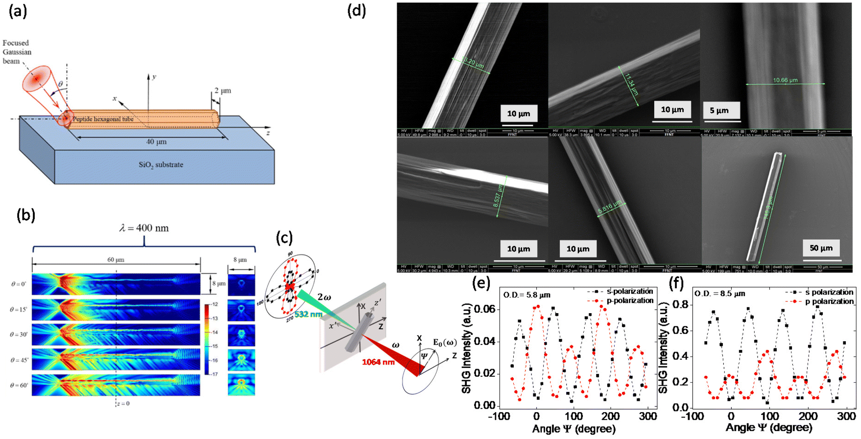 | ||
| Fig. 2 Waveguiding and nonlinear optical properties of FF nanotube. (a) and (b) Illustrate the simulation of the nonlinear waveguiding effect where the fundamental wavelength of 800 nm is incident at different angles. Reprinted with permission from ref. 18, copyright 2007, Elsevier. (c) Schematic of an individual FF tube with the laboratory (XYZ) and the sample reference (x′y′z′) frame illustrating the phenomenon of SHG. (d) SEM images of individual FF tubes used for measuring second harmonic generation. (e) and (f) SHG polarimetry results from two individual FF tubes with different diameters for s- and p-polarization. Reprinted with permission from ref. 17, copyright 2017, Royal Society of Chemistry. | ||
SHG polarimetry, where the polarization of the incident light is changed (angle ψ in Fig. 2c) and the SHG intensity is measured in both s- and p-polarization, provides indirect information on the symmetry and structure of the system. We refer to details in ref. 16 and 17 on how to transpose the electric field and polarization components between the laboratory and sample reference frames, specifically for the symmetry of FF-MNS tubes. SHG polarimetry from individual FF self-assembled tubes with varying diameters (Fig. 2d) shows that the pattern of the p-polarization light changes with the tube diameter (Fig. 2e and f) whereas the s-polarization remains the same. These experiments determined the nonlinear d coefficients with d15, d31 being the transverse components, and d33 being the longitudinal component. The d31 component was found to be negative. One must bear in mind that the nonlinear d components are related to the piezoelectric components, as discussed in the next section, but are not the same.
Piezoelectric properties (2D and fluorinated FF)
Traditionally, piezoelectric materials, where an applied mechanical stress generates electricity, have relied on inorganic oxides such as PZT (Pb(Zr,T)O3). However, their high temperature sintering makes them incompatible with the biological environment. The piezoelectric property of FF-MNS is very attractive from the perspective of energy harvesting applications. Micro-electromechanical systems can benefit from nanoscale devices where freeform printing of self-assembled FF-MNS is particularly advantageous as the peptides can be conformed to specific shapes, for example 3D spirals maximize the piezoelectric effect.Piezo force microscopy (PFM), based on a scanning probe method, allows monitoring of both the phase and the amplitude of a response by applying a small ac signal between the cantilever tip and the bottom electrode upon which the sample is mounted, and by varying the DC bias on one of the electrodes. PFM yields information on the polarity of the domains contributing to the piezoresponse as well as the strength of the response. PFM measurements from an individual FF-based micro/nanotube (of 100 nm diameter) demonstrated the shear component of the piezoelectric tensor (d15) to be as high as 35 pm V−1,11 which is comparable to bulk lithium niobate. It should be noted that the effective d15 coefficient scales with the tube diameter.
Another mechanism for enhancing the NLO and piezoelectric effect in FF-MNS has been fluorination, where one ortho-hydrogen atom in each of the phenyl groups of FF was replaced by fluorine (Fig. 3a). A comparison of the PFM results from fluorinated and non-fluorinated FF tubes of similar outer diameter (2 μm) is shown in Fig. 3b and c. The d15 component of the piezoelectric tensor was found to be 50 pm V−1 for the non-fluorinated FF tube and was almost ten times higher for the fluorinated FF tube.65
 | ||
| Fig. 3 Piezoelectric properties. (a) Chemical structure of FF and fluorine substituted FF (2-fluoro-L-phenylalanyl-2-fluoro-L-phenylalanine) (Fl-FF). (b) Topography, phase, and amplitude images of FF and Fl-FF. (c) Local DC voltage amplitude loops (piezoelectric response) from FF and Fl-FF tubes at an AC voltage of 0.5 V. Reprinted with permission from ref. 65, copyright 2019, American Institute of Physics. (d) Top and side view of the bilayer of LDFF. Piezoelectric response of LDFF and LN using (e) DC voltage hysteresis loops measured at different AC voltages, and (f) AC voltage dependences on the amplitude. Reprinted with permission from ref. 15, copyright 2021, Wiley-VCH. | ||
Out-of-plane piezoelectricity has been further shown from 2D layered dipeptide crystals. Layered biomolecular FF crystals (LDFF) were synthesized by a co-assembly of two enantiomers.15 The top and side-view of the bilayer system are shown in Fig. 3d, where the bilayer thickness is 1.5 nm. The local piezoelectric properties measured using a PFM are shown in Fig. 3e and f. Along with the LDFF sample, a z-cut surface of a lithium niobate (LN) crystal was compared. The d33 component of the piezoelectric tensor in LDFF, which in this case is the out-of-plane component, was found to be 20 pm V−1. Since the FF bilayers are held by weak aromatic interaction in the crystal, these layers may be exfoliated chemically or mechanically for applications in sensors, actuators, and wearable devices.
Templates for organic electronics
The π-stacking interaction in FF-MNS promotes adsorption of molecules and fluorophores.66,67 This idea was explored in demonstrating FF-MNS as a scaffold for blue-emitting π-conjugated polymers belonging to the polyfluorene (PF) family.21 Here the polymer still acts as the active material for charge transport and the peptide provides a template for achieving polymer nanostructures. Khanra and co-workers functionalized FF-MNS with different side-chain substituted PFs (shown in the inset of Fig. 1c). A representative TEM image is shown in Fig. 4a. Di-octyl substituted side-chain PF (PF8) showed a higher binding affinity towards FF-MNS compared with ethyl-hexyl substituted side-chain PF due to the van der Waals interaction energy, as suggested by molecular dynamics simulations.21 Further, aging PF8 in a solvent, which produces fibre-like polymer structures, improves binding with the FF tubes. The FF-MNS:PF nanocomposites showed bright electroluminescence (EL) in light-emitting diode architectures (Fig. 4b). Here, the EL spectrum from the pristine PF polymer is compared with the nanocomposite (FF-MNS:PF8 (aged)) when used as an active layer. Moreover, such nanocomposite films are biodegradable by enzymatic action, opening up a path for a new generation of biocompatible materials for organic electronics.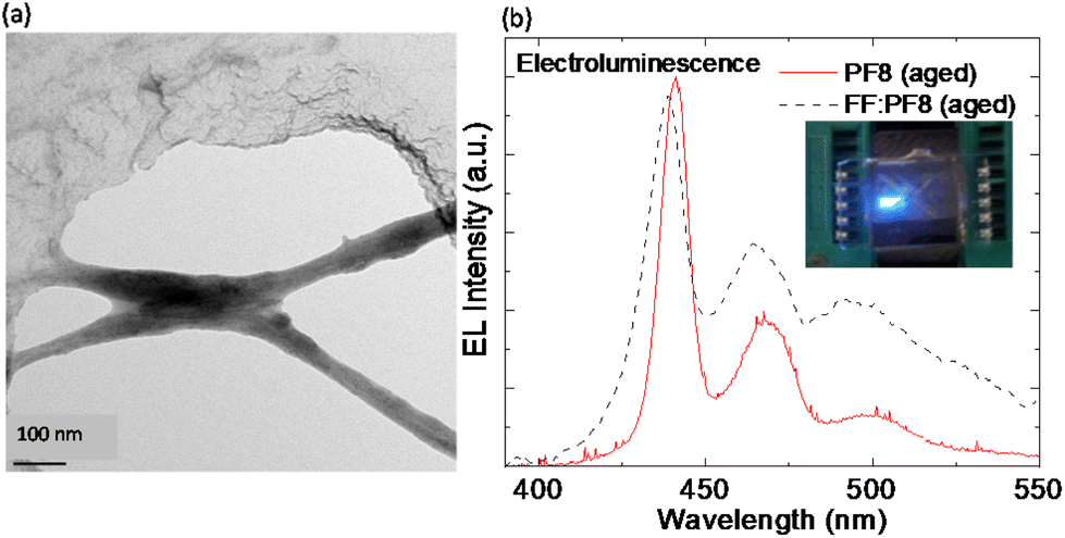 | ||
| Fig. 4 FF-MNS nanocomposites in light emission. (a) A representative TEM image from FF-MNS:PF8 nanocomposite. The dark region represents the polymer and the lighter region is the peptide tube. (b) Comparison of the EL spectrum of pristine PF8 (bold red line) with the FF-MNS:PF8 nanocomposite (black dotted line). In both cases the PF8 polymer was aged. The inset is an image of light emission from a PF8 light-emitting diode. Reprinted and adapted with permission from ref. 21, copyright 2015, Wiley-VCH. | ||
Among other applications of FF-MNS in organic electronics, using them in charge-modulated field-effect transistors (FETs) is particularly attractive. The peptide tubes can be easily integrated with the active semiconducting layer (typically π-conjugated molecule or polymer). Moreover, since FF-MNS can be easily functionalized with an antigen/antibody or an enzyme, FETs using FF-MNS, either as a dielectric layer or as a separate sensing area modulated by the FET, are attractive in biosensing for antibody–antigen or enzyme–analyte interaction.20
The π-stacking interaction in FF-MNS is favourable for binding with insulating magnetic nanoparticles such as cobalt ferrite (CFO). CFO nanoparticles bound to FF-MNS display enhanced magnetization properties due to a charge transfer process between the Fe2+ and Co2+ ions in CFO to the amine group of the peptide.22 The saturation magnetization is seen to increase by more than 20% in FF-MNS:CFO. An additional advantage of CFO incorporated FF-MNS is that it enhances the dielectric properties of FF-MNS, reducing the operating voltage of organic FETs.
FF-MNS functionalized with CFO as a dielectric layer in pentacene metal insulator semiconductor (MIS) diodes and FETs demonstrate enhanced capacitance.22 The accumulation capacitance is higher in a FF-MNS:CFO MIS diode compared to as-is FF-MNS (Fig. 5a and b). The thicknesses of the functionalized and the non-functionalized FF-MNS layers were similar in these devices. Since organic FETs mainly operate in the accumulation region (schematic architecture is shown in Fig. 5c), the accumulation capacitance governs the operating voltages in FETs. From the FET output characteristics plotted in Fig. 5d and e in pentacene FETs with as-is and CFO functionalized FF-MNS, it is clearly seen that the operating voltages are lowered in the latter. Since FF-MNS is also ferroelectric, such functionalized dielectrics provide opportunities in low operating voltage memory devices.
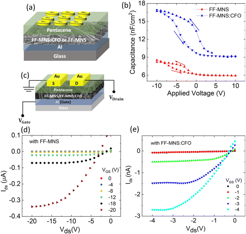 | ||
| Fig. 5 FF-MNS nanocomposites in transistors. (a) Schematic of a pentacene MIS diode. (b) Capacitance–voltage characteristics of pentacene MIS diodes using as-is FF-MNS and CFO functionalized FF-MNS dielectric layers. (c) Schematic of an FET. (d) and (e) Output characteristics of pentacene FETs with as-is FF-MNS and CFO functionalized FF-MNS dielectrics, respectively. Reprinted with permission from ref. 22, copyright 2018, American Chemical Society. | ||
The versatile application of FF-MNS as photonic and electronic elements brings to the fore the question of controlled alignment, formation of specific 3D structures in the nanoscale, and functionalization of these nanostructures other than with self-assembly, which inherently has limitations. The past few years have seen a tremendous growth of printed technologies for peptides and other biomaterials. 3D bioprinting,68,69 which can recreate tissues and organs reproducing physiologically relevant functions, has now become a reality. Peptide based hydrogels have shown promise as bioinks for 3D bioprinting and cell culture.70,71 In this minireview, our focus is on printed and patterned FF peptides, mainly for electronics and photonics application. Advances in 3D bioprinting are not reviewed here; we refer to the following ref. 70 and 72 for the development of short-peptide-based bioinks.
Printing technologies for self-assembled FF
Inkjet printing
The development of low-cost and flexible electronics depends on different forms of printing, amongst which inkjet printing is quite popular. It is a versatile technique for depositing conducting inks, solution-processable gate dielectric layers and active polymeric semiconducting layers in organic electronic circuits.73–78 This printing process relies on drop-on-demand piezo inkjet printheads where the precision of the jetting fluid can be controlled by applying an external voltage to the piezoelectric actuator.79 A pressure wave is formed in the capillary tube holding the ink, and upon reaching the nozzle, droplets are ejected as long as the kinetic energy transferred to the fluid is greater than the energy required for its formation. The jetting waveform, nozzle temperature, and substrate temperature must be adjusted for each ink. Moreover, the solvents must be carefully chosen to avoid nozzle blockage, which has been an issue in printing peptides due to the use of high viscous solvents.By choosing appropriate solvents and surfactants to change the rheological properties of FF solution, Safaryan and co-workers have demonstrated a new conformation of inkjet-printed FF crystals in the form of microribbons, which show a strong piezoelectric response.25 The FF solution in this printing process was prepared in acetic acid and diluted in ethanol and double-distilled water. Using a mixture of ethylene glycol and cationic surfactant, the viscosity of the ink was adjusted for optimized printing. The optical images of printed line-forms of FF are shown in Fig. 6a and b.
 | ||
| Fig. 6 Inkjet printing of FF. (a) Optical images of inkjet printed lineform based on FF solution. (b) The FF crystals grow perpendicular to the direction of printing. (c) Hydrodynamic parameters for printing FF. The Z value, which is the inverse of the Ohnesorge number, defines the printable zone. Reprinted with permission from ref. 25, copyright 2018, American Chemical Society. | ||
The choice of the hydrodynamic parameters determines the jetting condition of the FF ink. A direct correlation is seen between the Ohnesorge number (Oh), a measure of the viscous to internal and surface tension forces, and Reynold's number (R), a dimensionless parameter. R = ρVd/η, where ρ is the density of the ink, V is the velocity, d is the diameter of the drop, and η is the viscosity. Fig. 6c represents the printable zone on the Oh vs. R plot for the FF ink, where Z is the inverse of Oh. The optimum value for printing is when Z is between 1 and 10.80
The above example demonstrates the viability of inkjet printing FF nanostructures and opens avenues for changing the crystal structure, and thus some of the fundamental properties of FF beyond what is obtained from self-assembly. However, inkjet printing has limitations. The spatial resolution is typically in the tens of μm since it is limited by the nozzle diameter and the waveform, and flat surfaces are required for uniform deposition conditions. With advances in 3D printing, there are opportunities for molecular-level control for engineering nanoscale properties and devices. Below, we discuss one method for 3D printing of FF-MNS and prospects of generalizable patterning of biological structures, in general, at the nanoscale.
Meniscus-guided 3D printing
Meniscus-driven printing is an effective strategy for forming 3D nanostructures.28,81–83 Using nanopipettes and applying a high voltage between the substrate and the pipette, this non-contact method allows dispensing of fluids by creating an ink meniscus. Translating the ink meniscus in three dimensions by stepper motors under rapid evaporation forms 3D nanostructures. It should be kept in mind that several commercial 3D bioprinters operate on the principle of meniscus-guided printing but the printing is on a large length-scale. Printing of liquid metal for soft electronic circuits was recently demonstrated using such a commercial bioprinter.84Using the principle of meniscus-guided 3D printing along with the scheme of self-assembly in FF, Yang and co-workers have successfully printed FF-based 3D freeform micro/nanostructures with a spatial resolution of 12 μm in the lateral direction and a height of 200 nm. The FF ink was prepared with acetic acid and hydrochloric acid, providing the consistency of a Newtonian fluid, where the viscosity and the concentration are linearly related. In this method, micropipettes were used along with an elevated temperature of the substrate (70 °C). The printing is achieved in two steps; first, the femtoliter (fl) ink meniscus that is formed rapidly evaporates near the substrate and second, self-assembly of the deposited FF was promoted by heating the substrate at 110 °C (Fig. 7a(i) and (ii)). The optical images in Fig. 7b–e are a guide to the printing process, where the micropipette first touches the surface, the fl ink wets the substrate and forms the meniscus, and then lateral guiding allows line-forms of FF. Layer-by-layer repeated guiding of the meniscus ultimately results in 3D nano/micro architectures.
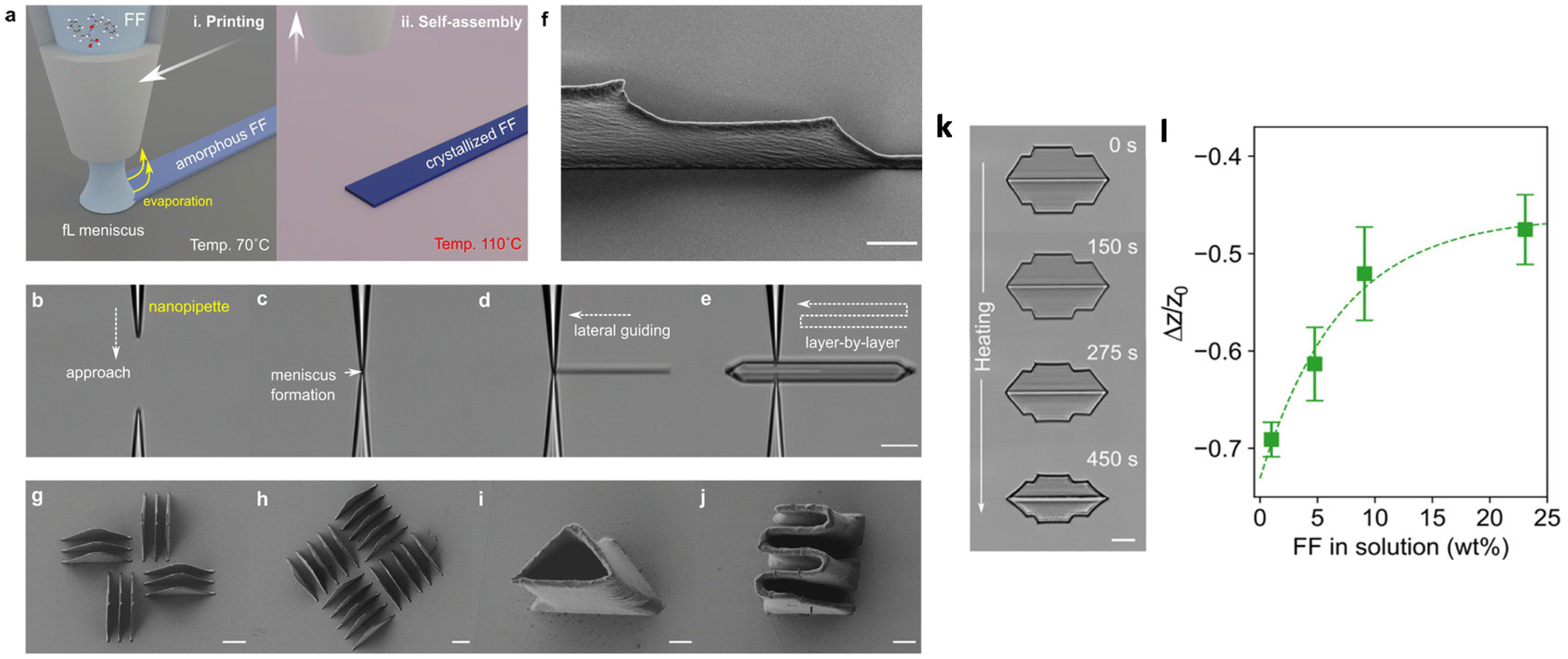 | ||
| Fig. 7 Meniscus-guided 3D printing. (a) Schematic of the printing process with (i) femtoliter (fl) ink meniscus which rapidly evaporates, depositing amorphous FF, and (ii) crystallization of FF at 110 °C. (b)–(e) Optical images of the printing process, starting with a glass micropipette approaching the substrate, fl ink wetting the substrate and forming the meniscus, and deposition of lineforms and layer-by-layer printing. (f) and (g–j) SEM images of the FF printed microstructures. In (f), the scale bar is 20 μm, and in (g–j), the scale bar is 5 μm. (k) Optical micrographs illustrating the geometrical changes in printed FF as a function of the annealing temperature. The scale bar is 20 μm. (l) Ratio of the change in height (Δz) to the as-is printed height (z0) of a printed structure as a function of FF concentration. Reprinted with permission from ref. 28, copyright 2021, American Chemical Society. | ||
By combining layer stacking and annealing, the width and the height of the FF structures could be controlled. Fig. 7k shows an example where the height of a FF wall decreases from 30 μm to 20 μm as the annealing time increases to 450 s. The reduction in the height can be further controlled by the FF concentration, as shown in Fig. 7l. A highly concentrated solution maintains the 3D shape. A significant piezoresponse was also observed from the annealed 3D FF structures.
The two examples of printed FF-MNS presented above highlight the precise composition of the inks that are required. Not only is there some trial and error in these approaches but it makes the entire printing process quite cumbersome. At some level, the process of self-assembly is more straightforward and controlled since the exact structure of FF-MNS (tubes, vesicles, floral shape etc.) can be determined by the nature of the solvent, the PH value, and temperature. The question then arises whether there is any nanofabrication technique available, which will enable nano-sculpturing the self-assembled peptide structures, to attain freeform assemblies at the nanoscale. Such a technique may then well be used for functionalizing FF-MNS, for example precise nanopatterning of metallic shapes on the tubes for application in nanophotonics. This may sound like science fiction but such a technique exists, except, thus far, it has not been applied to delicate biological structures. In the following section, we present future prospects for patterning FF-MNS and other self-assembled peptide structures using sacrificial ice resists.
Future prospects: ice lithography
The ultimate functionality of biological micro-nanostructures can be enhanced and fine-tuned via patterning. In principle, metallic, semiconducting, or insulating materials can be added to existing structures in a precise and deterministic manner using electron beam lithography followed by deposition.85 Alternatively, material can be subtracted via electron beam lithography followed by etching. However, in practice, any patterning of delicate 3D micro-nanostructures such as FF-MNS presents significant challenges.30 Innovative techniques are required to advance this frontier area of nanofabrication.Patterning challenges stem from two primary sources: (i) the complex 3D topology of the micro-nanostructure itself and (ii) the delicate nature of the bonds holding the structure together. Electron beam and other established lithography methods are well suited for patterning optically flat 2D hard condensed matter substrates, such as silicon wafers. Yet, spinning liquid phase resist does not produce uniform coating on non-planar surfaces. Furthermore, even if uniformity can be achieved, biological structures are easily damaged by the chemicals required for patterning, typically: anisole, for resist casting; methyl isobutyl ketone/isopropanol for resist developing; and acetone for resist removing.30
Researchers have developed a handful of processes to surmount patterning challenges, and an ideal solution would minimize chemical and hydrodynamic/mechanical perturbations to the delicate 3D biological structures. Float,86 spray,87 brush,88 and thermally evaporative resist coating techniques89,90 have all shown promise for patterning 3D micro-nanostructures comprised of hard condensed matter, such as atomic force microscopy cantilevers, which are held together via covalent bonds. But these methods employ perturbative processing steps, such as wet chemical developers. Hence, they are not well suited for soft material systems, such as FF-MNS, in which hydrogen bonding, hydrophobic, and van der Waals interactions underly the structural integrity. Patterning delicate biological structures requires a different approach.
Ice lithography is a nanopatterning method which employs solid-phase condensed gasses, such as amorphous water ice, as sacrificial resist for electron beam lithography.33,38Fig. 8a shows a potential example of patterning Au islands onto an FF tube using water ice resist. The method has demonstrated high precision (<10 nm) patterning on non-planar substrates. Fig. 8b shows an example of patterning metal nanoparticles on a suspended Ag wire using water ice resist.32 Local resist exposure/removal (e.g., via sublimation) can be followed by metallization and liftoff, which occurs by heating the sample, typically from the liquid nitrogen range to room temperature.91 This phase-transition – based patterning technique can completely avoid all solvents. Indeed, patterning can be performed without any fluid processing steps.35 All steps can be monitored in situ, leading to high yield fabrication and re-processing, if necessary. Hence, ice lithography offers a generalizable path for patterning delicate, free-standing, or three-dimensional structures including biological micro-nanostructures that can be easily damaged if exposed to conventional resists. Note that biological molecules are robust to freezing and thawing and can maintain near-native biochemical activity when adhered to surfaces, as is required for lithography.92,93 Exposure to cryogenic temperatures and near-by substrate surfaces do not preclude active nanopatterned structures.
 | ||
| Fig. 8 Ice lithography. (a) Illustration of patterning metal islands onto FF-MNS using water ice resist. (b) Array of metal nanoparticles patterned on an Ag nanowire (160 nm diameter) using electron-beam ice lithography, top (green frame) and side view (blue frame). The Ag nanowire shown in the red frame is after electron beam exposure but prior to metallization. The scale bar is 300 nm. Reprinted with permission from ref. 32, copyright 2018, American Chemical Society. | ||
Despite advantages, ice lithography using electron beam exposure is not devoid of shortcomings. Electron radiation can damage cryogenically fixed biological material by generating free radicals in the ice which can react with embedded biomolecules.94 This effect can be monitored and potentially mitigated, for example, by varying the electron beam energy and/or the ice species. Nonetheless, developing alternative ice lithography tools explicitly tailored for patterning soft material systems will be prudent. An appealing avenue would be to combine the advantages of ice resist (uniform coating of delicate 3D biological structures, completely dry solvent-free processing, in situ inspection and reprocessing) with a low-energy exposure mechanism, such as a scanning probe microscope tip.95 Time will tell, but this combination of methodology has the potential to achieve near-atomic precision patterning of delicate 3D biological micro-nanostructures.
Summary
Peptide nanomaterials have an exciting future in electronics and photonics applications. Their self-assembling properties have been heavily exploited in a variety of nano-architectures for energy generation, biosensing, and nanophotonics. However, freeform shapes at the nanoscale are difficult to achieve solely based on the process of self-assembly. By focussing on a short dipeptide (FF), we briefly summarize the process of self-assembly and applications in organic electronics and nonlinear optics in this minireview. Inkjet printing and other forms of 3D printing are viable avenues for precise freeform architectures but mainly at micron length scales. We speculate that other forms of nanopatterning techniques using ice resists may lead to a generalizable path towards precise 3D architectures of peptides at the micron and nano – length scales.Author contributions
All authors contributed to writing and preparing the manuscript.Conflicts of interest
There are no conflicts to declare.Acknowledgements
We thank our collaborators for their contribution to the development of peptide nanomaterials in electronics and generalized patterning. Without their insight and involvement, this minireview could not have been realized. The list is long; so, we acknowledge only a few key players in this endeavour. Thiago Cipriano, Soma Khanra, and Grant Knotts laid the foundation for peptide nanostructures as templates in organic electronics. We thank Eudes Fileti for providing insights into the self-assembly process and interaction of conjugated polymers with peptides. Rainer Glaser and Sandra Vassiliades demonstrated the significance of fluorinated FF. Kartik Ghosh and Ping Yu were involved in determining the piezoelectric and NLO properties, respectively.SG and GK acknowledge the support of the U.S. National Science Foundation under Grant No. ECCS #2064337 for facilitating a workshop to identify ice lithography as a promising pathway for achieving high resolution patterning.
References
- A. Levin, T. A. Hakala, L. Schnaider, G. J. L. Bernardes, E. Gazit and T. P. J. Knowles, Nat. Rev. Chem., 2020, 4, 615–634 CrossRef CAS.
- M. Reches and E. Gazit, Science, 2003, 300, 625–627 CrossRef CAS PubMed.
- J. Wang, K. Liu, R. Xing and X. Yan, Chem. Soc. Rev., 2016, 45, 5589–5604 RSC.
- N. Kol, L. Adler-Abramovich, D. Barlam, R. Z. Shneck, E. Gazit and I. Rousso, Nano Lett., 2005, 5, 1343–1346 CrossRef CAS PubMed.
- M. S. Liberato, S. Kogikoski, E. R. da Silva, D. R. de Araujo, S. Guha and W. A. Alves, J. Mater. Chem. B, 2016, 4, 1405–1413 RSC.
- L. Schnaider, S. Brahmachari, N. W. Schmidt, B. Mensa, S. Shaham-Niv, D. Bychenko, L. Adler-Abramovich, L. J. W. Shimon, S. Kolusheva, W. F. DeGrado and E. Gazit, Nat. Commun., 2017, 8, 1365 CrossRef PubMed.
- M. Ni and S. Zhuo, RSC Adv., 2019, 9, 844–852 RSC.
- B. B. Gerbelli, S. V. Vassiliades, J. E. U. Rojas, J. N. B. D. Pelin, R. S. N. Mancini, W. S. G. Pereira, A. M. Aguilar, M. Venanzi, F. Cavalieri, F. Giuntini and W. A. Alves, Macromol. Chem. Phys., 2019, 220, 1900085 CrossRef.
- S. Kogikoski, C. P. Sousa, M. S. Liberato, T. Andrade-Filho, T. Prieto, F. F. Ferreira, A. R. Rocha, S. Guha and W. A. Alves, Phys. Chem. Chem. Phys., 2016, 18, 3223–3233 RSC.
- X. Yan, P. Zhu and J. Li, Chem. Soc. Rev., 2010, 39, 1877–1890 RSC.
- A. Kholkin, N. Amdursky, I. Bdikin, E. Gazit and G. Rosenman, ACS Nano, 2010, 4, 610–614 CrossRef CAS PubMed.
- I. Bdikin, V. Bystrov, S. Kopyl, R. P. G. Lopes, I. Delgadillo, J. Gracio, E. Mishina, A. Sigov and A. L. Kholkin, Appl. Phys. Lett., 2012, 100, 043702 CrossRef.
- A. Handelman, P. Beker, N. Amdursky and G. Rosenman, Phys. Chem. Chem. Phys., 2012, 14, 6391–6408 RSC.
- K. Ryan, J. Beirne, G. Redmond, J. I. Kilpatrick, J. Guyonnet, N.-V. Buchete, A. L. Kholkin and B. J. Rodriguez, ACS Appl. Mater. Interfaces, 2015, 7, 12702–12707 CrossRef CAS PubMed.
- P. S. Zelenovskii, K. Romanyuk, M. S. Liberato, P. Brandão, F. F. Ferreira, S. Kopyl, L. M. Mafra, W. A. Alves and A. L. Kholkin, Adv. Funct. Mater., 2021, 31, 2102524 CrossRef CAS.
- A. Handelman, S. Lavrov, A. Kudryavtsev, A. Khatchatouriants, Y. Rosenberg, E. Mishina and G. Rosenman, Adv. Opt. Mater., 2013, 1, 875–884 CrossRef.
- S. Khanra, K. Ghosh, F. F. Ferreira, W. A. Alves, F. Punzo, P. Yu and S. Guha, Phys. Chem. Chem. Phys., 2017, 19, 3084–3093 RSC.
- A. Handelman, B. Apter, N. Turko and G. Rosenman, Acta Biomater., 2016, 30, 72–77 CrossRef CAS PubMed.
- Q. Li, Y. Jia, L. Dai, Y. Yang and J. Li, ACS Nano, 2015, 9, 2689–2695 CrossRef CAS PubMed.
- T. Cipriano, G. Knotts, A. Laudari, R. C. Bianchi, W. A. Alves and S. Guha, ACS Appl. Mater. Interfaces, 2014, 6, 21408–21415 CrossRef CAS PubMed.
- S. Khanra, T. Cipriano, T. Lam, T. A. White, E. E. Fileti, W. A. Alves and S. Guha, Adv. Mater. Interfaces, 2015, 2, 1500265–1500274 CrossRef.
- S. Khanra, M. Abdullah-Al Mamun, F. F. Ferreira, K. Ghosh and S. Guha, ACS Appl. Nano Mater., 2018, 1, 1175–1187 CrossRef CAS.
- Z. A. Arnon, A. Vitalis, A. Levin, T. C. T. Michaels, A. Caflisch, T. P. J. Knowles, L. Adler-Abramovich and E. Gazit, Nat. Commun., 2016, 7, 13190 CrossRef CAS PubMed.
- L. Adler-Abramovich and E. Gazit, J. Pept. Sci., 2008, 14, 217–223 CrossRef CAS PubMed.
- S. Safaryan, V. Slabov, S. Kopyl, K. Romanyuk, I. Bdikin, S. Vasilev, P. Zelenovskiy, V. Y. Shur, E. A. Uslamin, E. A. Pidko, A. V. Vinogradov and A. L. Kholkin, ACS Appl. Mater. Interfaces, 2018, 10, 10543–10551 CrossRef CAS PubMed.
- L. Persano, A. Camposeo, P. D. Carro, V. Fasano, M. Moffa, R. Manco, S. D'Agostino and D. Pisignano, Adv. Mater., 2014, 26, 6542–6547 CrossRef CAS PubMed.
- L. Adler-Abramovich, D. Aronov, P. Beker, M. Yevnin, S. Stempler, L. Buzhansky, G. Rosenman and E. Gazit, Nat. Nanotechnol., 2009, 4, 849–854 CrossRef CAS PubMed.
- J. Yang, M. Chen, H. Lee, Z. Xu, Z. Zhou, S.-P. Feng and J. T. Kim, ACS Appl. Mater. Interfaces, 2021, 13, 20573–20580 CrossRef CAS PubMed.
- R. M. M. Hasan and X. Luo, Nanomanuf. Metrol., 2018, 1, 67–81 CrossRef.
- A. K. Grebenko, K. A. Motovilov, A. V. Bubis and A. G. Nasibulin, Small, 2022, 18, 2200476 CrossRef CAS PubMed.
- A. Elsukova, A. Han, D. Zhao and M. Beleggia, Nano Lett., 2018, 18, 7576–7582 CrossRef CAS PubMed.
- Y. Hong, D. Zhao, D. Liu, B. Ma, G. Yao, Q. Li, A. Han and M. Qiu, Nano Lett., 2018, 18, 5036–5041 CrossRef CAS PubMed.
- D. Zhao, A. Han and M. Qiu, Sci. Bull., 2019, 64, 865–871 CrossRef.
- Y. Hong, D. Zhao, J. Wang, J. Lu, G. Yao, D. Liu, H. Luo, Q. Li and M. Qiu, Nano Lett., 2020, 20, 8841–8846 CrossRef CAS PubMed.
- G. Yao, D. Zhao, Y. Hong, S. Wu, D. Liu and M. Qiu, Nanoscale, 2020, 12, 22473–22477 RSC.
- D. Zhao, B. Chang and M. Beleggia, ACS Appl. Mater. Interfaces, 2020, 12, 6436–6441 CrossRef CAS PubMed.
- R. Zheng, D. Zhao, Y. Lu, S. Wu, G. Yao, D. Liu and M. Qiu, Adv. Funct. Mater., 2022, 32, 2112894 CrossRef CAS.
- G. M. King, G. Schürmann, D. Branton and J. A. Golovchenko, Nano Lett., 2005, 5, 1157–1160 CrossRef CAS PubMed.
- I. W. Hamley, Chem. Rev., 2012, 112, 5147–5192 CrossRef CAS PubMed.
- V. F. M. Segers and R. T. Lee, Drug Discovery, 2007, 12, 561–568 CAS.
- G. Wei, Z. Su, N. P. Reynolds, P. Arosio, I. W. Hamley, E. Gazit and R. Mezzenga, Chem. Soc. Rev., 2017, 46, 4661–4708 RSC.
- B. B. Gerbelli, C. L. P. Oliveira, E. R. Silva, I. W. Hamley and W. A. Alves, Langmuir, 2020, 36, 14793–14801 CrossRef CAS PubMed.
- C. C. Decandio, E. R. Silva, I. W. Hamley, V. Castelletto, M. S. Liberato, V. X. Oliveira, C. L. P. Oliveira and W. A. Alves, Langmuir, 2015, 31, 4513–4523 CrossRef CAS PubMed.
- M. R. Sawaya, S. Sambashivan, R. Nelson, M. I. Ivanova, S. A. Sievers, M. I. Apostol, M. J. Thompson, M. Balbirnie, J. J. W. Wiltzius, H. T. McFarlane, A. Ø. Madsen, C. Riekel and D. Eisenberg, Nature, 2007, 447, 453–457 CrossRef CAS PubMed.
- A. Aggeli, I. A. Nyrkova, M. Bell, R. Harding, L. Carrick, T. C. B. McLeish, A. N. Semenov and N. Boden, Proc. Natl. Acad. Sci. U. S. A., 2001, 98, 11857–11862 CrossRef CAS PubMed.
- S. Sharpe, K. Simonetti, J. Yau and P. Walsh, Biomacromolecules, 2011, 12, 1546–1555 CrossRef CAS PubMed.
- A. K. Mehta, K. Lu, W. S. Childers, Y. Liang, S. N. Dublin, J. Dong, J. P. Snyder, S. V. Pingali, P. Thiyagarajan and D. G. Lynn, J. Am. Chem. Soc., 2008, 130, 9829–9835 CrossRef CAS PubMed.
- P. Tamamis, L. Adler-Abramovich, M. Reches, K. Marshall, P. Sikorski, L. Serpell, E. Gazit and G. Archontis, Biophys. J., 2009, 96, 5020–5029 CrossRef CAS PubMed.
- R. Huang, R. Su, W. Qi, J. Zhao and Z. He, Nanotechnology, 2011, 22, 245609 CrossRef PubMed.
- P. Kumaraswamy, R. Lakshmanan, S. Sethuraman and U. M. Krishnan, Soft Matter, 2011, 7, 2744–2754 RSC.
- C. H. Görbitz, Chem. Commun., 2006, 2332–2334, 10.1039/B603080G.
- X. Yan, Y. Cui, Q. He, K. Wang and J. Li, Chem. Mater., 2008, 20, 1522–1526 CrossRef CAS.
- T. Andrade-Filho, F. F. Ferreira, W. A. Alves and A. R. Rocha, Phys. Chem. Chem. Phys., 2013, 15, 7555–7559 RSC.
- P. M. G. L. Ferreira, M. S. Ishikawa, S. Kogikoski, W. A. Alves and H. Martinho, Phys. Chem. Chem. Phys., 2015, 17, 32126–32131 RSC.
- T. Andrade-Filho, T. C. Martins, F. F. Ferreira, W. A. Alves and A. R. Rocha, Theor. Chem. Acc., 2016, 135, 185 Search PubMed.
- J. Kim, T. H. Han, Y.-I. Kim, J. S. Park, J. Choi, D. G. Churchill, S. O. Kim and H. Ihee, Adv. Mater., 2010, 22, 583–587 CrossRef CAS PubMed.
- R. C. Bianchi, E. R. da Silva, L. H. Dall'Antonia, F. F. Ferreira and W. A. Alves, Langmuir, 2014, 30, 11464–11473 CrossRef CAS PubMed.
- G. Demirel and F. Buyukserin, Langmuir, 2011, 27, 12533–12538 CrossRef CAS PubMed.
- Y. Su, X. Yan, A. Wang, J. Fei, Y. Cui, Q. He and J. Li, J. Mater. Chem., 2010, 20, 6734–6740 RSC.
- J. Ryu and C. B. Park, Adv. Mater., 2008, 20, 3754–3758 CrossRef CAS.
- H. R. Amaral, S. Kogikoski, E. R. Silva, J. A. Souza and W. A. Alves, Mater. Chem. Phys., 2012, 137, 628–636 CrossRef CAS.
- M. S. Liberato, S. Kogikoski, E. R. Silva, M. D. Coutinho-Neto, L. P. B. Scott, R. H. Silva, V. X. Oliveira, R. A. Ando and W. A. Alves, J. Phys. Chem. B, 2013, 117, 733–740 CrossRef CAS PubMed.
- X. Liu, J. Danglad-Flores, S. Eickelmann, B. Sun, J. Hao, H. Riegler and J. Li, ACS Nano, 2022, 16, 10372–10382 CrossRef CAS PubMed.
- Q. Li, H. Ma, A. Wang, Y. Jia, L. Dai and J. Li, Adv. Opt. Mater., 2015, 3, 194–198 CrossRef CAS.
- S. Khanra, S. V. Vassiliades, W. A. Alves, K. Yang, R. Glaser, K. Ghosh, P. Bhattacharya, P. Yu and S. Guha, AIP Adv., 2019, 9, 115202 CrossRef.
- T. D. Martins, M. I. de Souza, B. B. Cunha, P. M. Takahashi, F. F. Ferreira, J. A. Souza, E. E. Fileti and W. A. Alves, J. Phys. Chem. C, 2011, 115, 7906–7913 CrossRef CAS.
- M. I. Souza, Y. M. Jaques, G. P. de Andrade, A. O. Ribeiro, E. R. da Silva, E. E. Fileti, É. d. S. Ávilla, M. V. B. Pinheiro, K. Krambrock and W. A. Alves, J. Phys. Chem. B, 2013, 117, 2605–2614 CrossRef CAS PubMed.
- F. Pati, J. Gantelius and H. A. Svahn, Angew. Chem., Int. Ed., 2016, 55, 4650–4665 CrossRef CAS PubMed.
- N. Hong, G.-H. Yang, J. Lee and G. Kim, J. Biomed. Mater. Res., Part B, 2018, 106, 444–459 CrossRef CAS PubMed.
- H. Jian, M. Wang, Q. Dong, J. Li, A. Wang, X. Li, P. Ren and S. Bai, ACS Appl. Mater. Interfaces, 2019, 11, 46419–46426 CrossRef CAS PubMed.
- X.-Q. Dou and C.-L. Feng, Adv. Mater., 2017, 29, 1604062 CrossRef PubMed.
- K. Tao, A. Levin, L. Adler-Abramovich and E. Gazit, Chem. Soc. Rev., 2016, 45, 3935–3953 RSC.
- B.-J. de Gans, P. C. Duineveld and U. S. Schubert, Adv. Mater., 2004, 16, 203–213 CrossRef CAS.
- H. Sirringhaus, T. Kawase, R. H. Friend, T. Shimoda, M. Inbasekaran, W. Wu and E. P. Woo, Science, 2000, 290, 2123–2126 CrossRef CAS PubMed.
- P. Calvert, Chem. Mater., 2001, 13, 3299–3305 CrossRef CAS.
- S. Chung, S. O. Kim, S. Kwon, C. Lee and Y. Hong, IEEE Electron Device Lett., 2011, 32, 1134–1136 CAS.
- F. J. Pavinatto, C. W. A. Paschoal and A. C. Arias, Biosens. Bioelectron., 2015, 67, 553–559 CrossRef CAS PubMed.
- K. Gooden, A. Laudari, G. Knotts and S. Guha, Flexible Printed Electron., 2016, 1, 015004 CrossRef.
- E. Tekin, P. J. Smith and U. S. Schubert, Soft Matter, 2008, 4, 703–713 RSC.
- D. Jang, D. Kim and J. Moon, Langmuir, 2009, 25, 2629–2635 CrossRef CAS PubMed.
- M. Chen, Z. Xu, J. H. Kim, S. K. Seol and J. T. Kim, ACS Nano, 2018, 12, 4172–4177 CrossRef CAS PubMed.
- M. Chen, J. Yang, Z. Wang, Z. Xu, H. Lee, H. Lee, Z. Zhou, S.-P. Feng, S. Lee, J. Pyo, S. K. Seol, D.-K. Ki and J. T. Kim, Adv. Mater., 2019, 31, 1904073 CrossRef CAS PubMed.
- Y. Liu, J. Yang, C. Tao, H. Lee, M. Chen, Z. Xu, H. Peng, X. Huan, J. Li, X. Cheng and J. T. Kim, ACS Appl. Mater. Interfaces, 2022, 14, 7184–7191 CrossRef CAS PubMed.
- G.-H. Lee, Y. R. Lee, H. Kim, D. A. Kwon, H. Kim, C. Yang, S. Q. Choi, S. Park, J.-W. Jeong and S. Park, Nat. Commun., 2022, 13, 2643 CrossRef CAS PubMed.
- P. Rai-Choudhury, Microlithography, 1997, 1, 139–249 Search PubMed.
- H. Zhou, B. K. Chong, P. Stopford, G. Mills, A. Midha, L. Donaldson and J. M. R. Weaver, J. Vac. Sci. Technol., B, 2000, 18, 3594–3599 CrossRef CAS.
- J. Linden, C. Thanner, B. Schaaf, S. Wolff, B. Lagel and E. Oesterschulze, Microelectron. Eng., 2011, 88, 2030–2032 CrossRef CAS.
- F. Aydinoglu, H. Yamada, R. K. Dey and B. Cui, Langmuir, 2017, 33, 4981–4985 CrossRef CAS PubMed.
- R. Swami, G. Julie, D. Singhal, J. Paterson, J. Maire, S. Le-Denmat, J. F. Motte, S. Gomes and O. Bourgeois, Nano Futures, 2022, 6, 025005 CrossRef.
- J. Zhang, C. Con and B. Cui, ACS Nano, 2014, 8, 3483–3489 CrossRef CAS PubMed.
- A. P. Han, A. Kuan, J. Golovchenko and D. Branton, Nano Lett., 2012, 12, 1018–1021 CrossRef CAS PubMed.
- K. Chattrakun, D. P. Hoogerheide, C. Mao, L. L. Randall and G. M. King, Langmuir, 2019, 35, 12246–12256 CrossRef CAS PubMed.
- N. Chada, K. Chattrakun, B. P. Marsh, C. F. Mao, P. Bariya and G. M. King, Sci. Adv., 2018, 4, eaat8797 CrossRef CAS PubMed.
- R. M. Glaeser and K. A. Taylor, J. Microsc., 1978, 112, 127–138 CrossRef CAS PubMed.
- R. Garcia, A. W. Knoll and E. Riedo, Nat. Nanotechnol., 2014, 9, 577–587 CrossRef CAS PubMed.
| This journal is © The Royal Society of Chemistry 2022 |