
 Open Access Article
 This Open Access Article is licensed under a Creative Commons Attribution-Non Commercial 3.0 Unported Licence
Perspective on the scintillating response of CdSe based nanoplatelets heterostructures†
Zhu
Meng
a,
Benoit
Mahler
 *a,
Julien
Houel
a,
Florian
Kulzer
a,
Andrey
Vasil'ev
b and
Christophe
Dujardin
*a
*a,
Julien
Houel
a,
Florian
Kulzer
a,
Andrey
Vasil'ev
b and
Christophe
Dujardin
*a
aInstitut Lumière Matière, UMR5306 Université Lyon 1-CNRS, Université de Lyon, 69622 Villeurbanne Cedex, France. E-mail: christophe.dujardin@univ-lyon1.fr; benoit.mahler@univ-lyon1.fr
bSkobeltsyn Institute of Nuclear Physics, Lomonosov Moscow State University, 119991 Moscow, Russia
First published on 14th September 2022
Abstract
We explore the effect of shell thickness on the time and spectral response of CdSe/CdS core–crown and CdSe/CdZnS core–shell nanoplatelets (NPLs) under X-ray and intense optical excitation. From their intensity-dependent spectral and timing response, we demonstrate that the exciton–exciton interaction in the bi-exciton (XX) changes from attractive to repulsive when varying the design from core/crown to thick quasi type II core/shell 2D nanostructures. We find that an additional shell layer of 0.4 nm is enough to convert the red-shifted XX emission to non- or blue-shifted emission. Under pulsed X-ray excitation, the scintillation decay dynamics reveal that multiexcitons are generated in all 2D nanostructures, whose presence can hardly be detected in the emission spectra for NPL thicknesses larger than 2 nm. We provide a numerical estimation of the number of scattering events of 35 keV electron as a function of NPL thickness, revealing that the formation of biexcitons with ultra-fast time response is more efficient in thick NPLs. However, this advantage is counterbalanced by a blue-shifted emission of that ultra-fast emission, rendering large NPLs less effective regarding the self-absorption issue.
1 Introduction
Colloidal semiconductor nanoplatelets (NPLs) have attracted a lot of attention due to their superior physical and chemical properties. Precise control on their thickness and confinement in one dimension leads to narrower emission spectra, larger absorption cross sections, and giant oscillator strengths,1,2 which are desired properties for various applications, including light-emitting diodes, low threshold lasing and solar cells.3–6 Additionally, their fast decay dynamics offer promising prospects for the fast-timing radiation detection,7,8 which can convert high energy photons (X-ray or γ-ray) or particles (electron, α,…) into visible light. Such a material is usually called a scintillator. The pursuit of fast-timing ability for high energy physics and time-of-flight positron emission tomography (TOF-PET) motivates the exploration of new scintillation materials9 and the strong quantum confinement in 2D of NPLs provides the opportunity to achieve the required time response. Furthermore, tunable emission spectra and processability in solution are additional required properties for scintillating materials based on nanostructures.10 Nevertheless, the stopping power for X-ray and γ photons depends on the total mass of the active material, which requires handling materials in bulky form or highly concentrated in mass in a matrix, or implementing strategies with hybrid materials where one component insures the stopping power and another contributes in part to the fast timing functionality, betting on an appropriate sharing of energy along the energy relaxation pathway. As an illustration, for CdSe nanoplatelets deposited on Lu2SiO5Ce3+ single crystal, the energy sharing has demonstrably improved the a coincidence time resolution,11 a crucial parameter for time-of-flight positron emission tomography. However, compared to core/shell nanostructures, this hybrid configuration exhibits the lack of proper passivation on their larger lateral surfaces and may still suffer from stability issues.12 In addition to that, the use of semiconducting NCs at very high concentrations is facing the self-absorption issue due to a small Stokes shift, which reduces of the light extraction efficiency. One strategy to overcome the self-absorption issue is to use core/shell NCs, allowing to increase the stopping power of the media while keeping constant the concentration of emitting centers and thus limit self-absorption. Finally, in spite of some preliminary results having been published, the physics underlying energy deposition, relaxation in NPLs as well as multi-exciton generation is still not fully understood in such 2D materials. To date, a study performed on CdSe quantum dots reported the generation of multi-excitons during the entire energy relaxation process following the electron excitation.13 In a recent work on spherical quantum wells, we have studied the effect of the particle dimension on the multi-exciton generation under X-ray excitation.14 In this contribution, we therefore explore and compare a series of 2D nanostructures made of alloyed CdSe/CdS core/crown (C/C) and CdSe/CdZnS core/shell (C/S) NPLs via the hot injection approach to realize a high emission quantum yield and high chemical stability in a nanoscintillator with a fast time response. Compared to the core/crown structure, the effective passivation of surface trap states by the epitaxial growth of wider-bandgap shells enhances the quantum yield and the stability. Furthermore, adjusting the thickness of the shell enables the investigation of size-dependent scintillating properties including multi-exciton generation. The alloyed composites give rise to the gradient energy band alignment, which is regarded as an efficient way to decrease Auger recombination.15 Here, through spectral and dynamical comparison under X-ray excitation and photoexcitation, we report the identification of excitation species produced during the energy relaxation process induced by X-rays, including single excitons and multi-excitons in NPLs, and we discuss the influence of shell thickness on the scintillation properties with respect to fast timing applications.2 Results and discussion
2.1 Nanoplatelets: synthesis and characterizations
Our aim is to synthesize different NPL heterostructures: core/crown (C/C) as well as core/shell (C/S) NPLs with different thicknesses to explore the underlying physics under X-rays excitation, and to compare their scintillation behaviors.All chemicals were used directly without purification.
![[thin space (1/6-em)]](https://www.rsc.org/images/entities/char_2009.gif) :9.3 g of Na(myristate) is dissolved in methanol under vigorous magnetic stirring for 1 h. 3.7 g of Cd(NO3)·4H2O dissolved in 120 mL MeOH is slowly added to this solution inducing Cd(myr)2 precipitation. After one more hour stirring, the white solid is filtered and washed multiple times on Buchner. TOPS 1 M: we prepared 1 M TOPS solution by dispersing 160.3 mg of sulfur into 5 mL of TOP. The solution was stirred overnight at room temperature in an air-free glovebox to ensure the S powder completely dissolved.
:1 ethanol:hexane mixture. The resulting C/C NPLs were finally redispersed in hexane. The TEM image of the C/C NPLs is presented in Fig. 1(a). The inset shows the NPLs thickness which is, as expected, smaller that the smallest thickness of the C/S NPLs. The C/C NPLs show a regular rectangular shape with lateral dimensions in the range of 25 nm for the length and 10 nm for the width.
:9.3 g of Na(myristate) is dissolved in methanol under vigorous magnetic stirring for 1 h. 3.7 g of Cd(NO3)·4H2O dissolved in 120 mL MeOH is slowly added to this solution inducing Cd(myr)2 precipitation. After one more hour stirring, the white solid is filtered and washed multiple times on Buchner. TOPS 1 M: we prepared 1 M TOPS solution by dispersing 160.3 mg of sulfur into 5 mL of TOP. The solution was stirred overnight at room temperature in an air-free glovebox to ensure the S powder completely dissolved.
:1 ethanol:hexane mixture. The resulting C/C NPLs were finally redispersed in hexane. The TEM image of the C/C NPLs is presented in Fig. 1(a). The inset shows the NPLs thickness which is, as expected, smaller that the smallest thickness of the C/S NPLs. The C/C NPLs show a regular rectangular shape with lateral dimensions in the range of 25 nm for the length and 10 nm for the width.
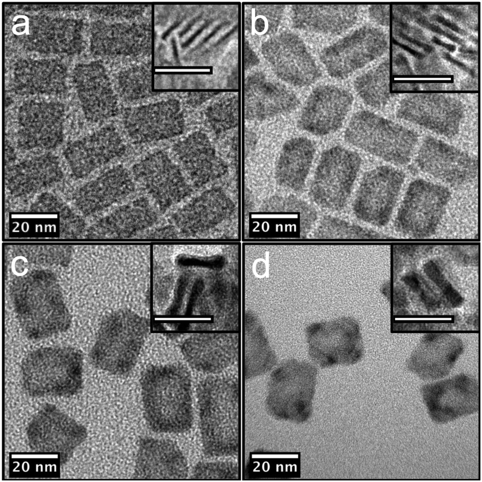 | ||
| Fig. 1 Transmission microscope images of the series of NPLs. (a) TEM images of core–crown NPLs. (b)–(d) are the core–shell NPLs with small, medium and large shell thicknesses. The insets show vertical NPLs, highlighting thickness changes. The scale bar is 20 nm. The NPLs thicknesses are 2 nm, 3 nm and 4 nm for images (b), (c) and (d) respectively. | ||
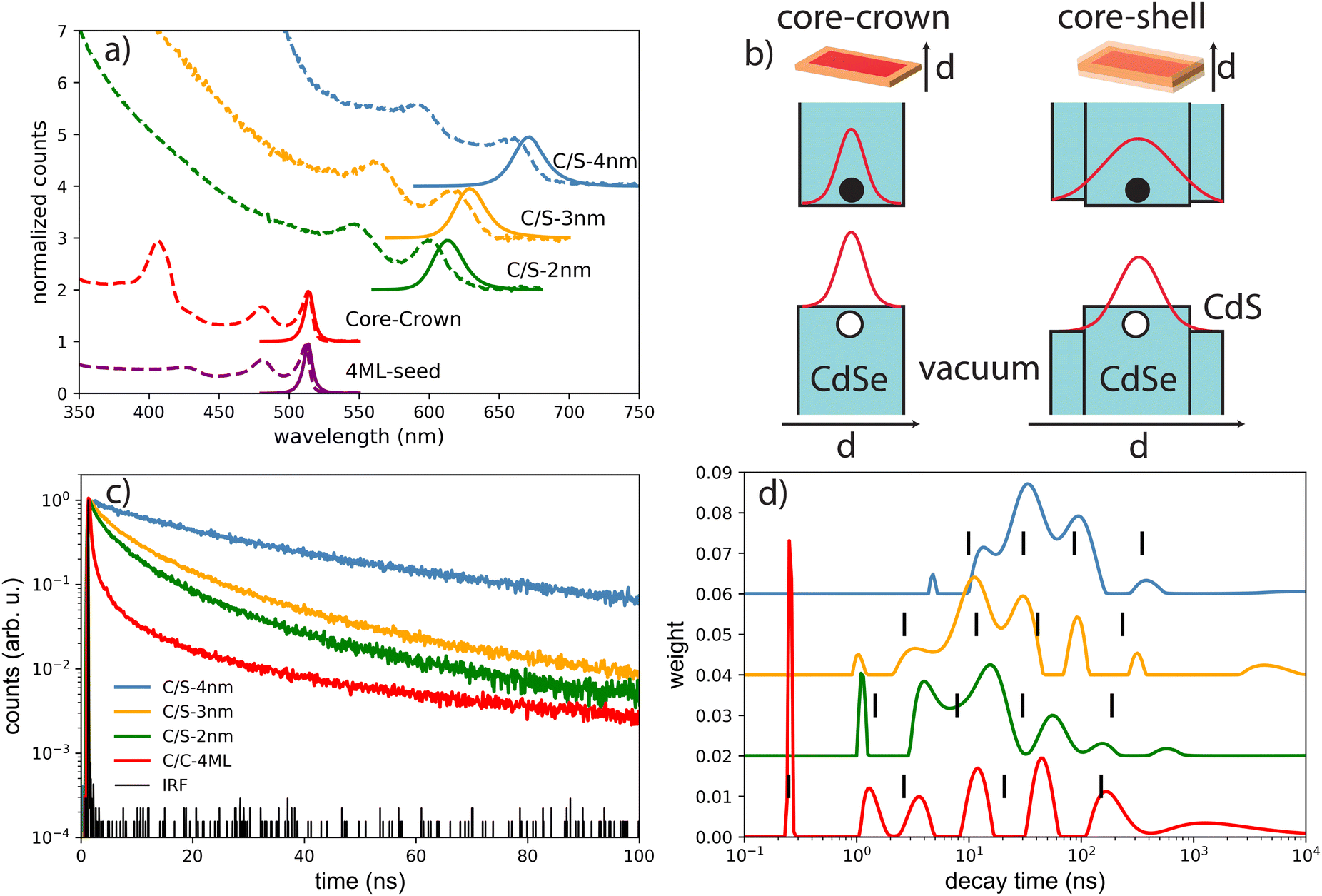 | ||
| Fig. 2 (a) Absorbance normalized to the first exciton (dashed) and normalized emission under 405 nm excitation of the NPLs samples in solution. (b) Schematic presentation of the energy band diagram of the C/C and C/S NPLs and the spread of the wavefunctions of electrons and holes (c) decay time measurement of the drop-casted NPLs on silicon substrates under low power excitation at 405 nm and (d) the deduced decay time distributions. Black lines correspond to the decay value obtained by a fitting performed with 4 exponential functions. | ||
The decay curves obtained under 405 nm at low power excitation (power 35 μW non focused) of samples consisting of a drop-cast from a colloidal solution of NPLs on a silicon substrate are presented in Fig. 2(c) for the C/C and C/S NPLs samples. We systematically adjust our initial NPL solutions to have an optical density of 20 at 350 nm. This value implies a concentration in Se of about 0.01 mmoL in 1 mL NPLs solution. We dilute these solutions 3 times and use them for film deposition. We generally use 10 μL of solution that we dry on a 10 × 10 mm silicon substrate to obtain the films. According to the known Se concentration, we can calculate the theoretical thickness of the film, and we obtain that under these conditions the homogeneous thin film is about 300 nm thick (considering that the NPLs plus ligands are about 3 nm thick), with a 100 nm CdSe active layer. The thickness of the NPLs layer was thus kept small enough to avoid self-absorption effects. The decay rate is driven by complex multiple-channel recombination of excitons, including single exciton radiative recombination, trap recombination and non-radiative recombination leading to multiexponential behavior20,21 including long components due to traps.22 The traditional fitting method with a small pre-defined number exponential components assumes that there are distinct mechanisms with well-defined characteristic times. This is not the case for various types of processes including quenching (typical example is dipole–dipole quenching), diffusion-controlled reactions, tunneling processes and nonlinear processes resulting in hyperbolic laws. The approximation of the decay using e.g. a stretched exponential (which is also the parametrization widely used for decays in nanostructured systems) is also not directly connected with specific decay mechanisms. We propose to use the fitting with a large set of exponential functions with quasi-continuous distribution of characteristic times and technical details are described in the ESI.† Because of this complex multi-exponential behaviour for all sizes, we have first applied a time-distribution fitting procedure where the experimental data have been adjusted by 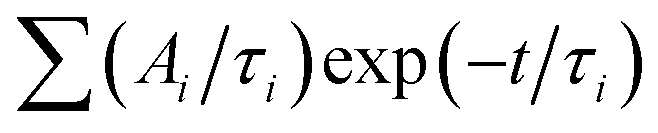 considering the instrumental response function and the excitation repetition rate. The τi are fixed as regularly distributed on a log scale, while the amplitudes Ai (weights of the corresponding exponents) are the free parameters and thus represent the fraction of photons contributing to each decay. Such a method is instructive in the case of complex decays allowing to show some maxima which are broadened by the size distributions of the samples as can be observed in Fig. 2(d). All samples exhibit a wide distribution of decay times ranging from sub-nanoseconds to several μs. The slow component can also be described as an hyperbolic power-law distribution revealing probably some tunneling processes from defects (Fig. SI-7, ESI†).
We can observe in the C/S that the lifetime gradually increases with shell thickness, which reflects that the relaxation of the quantum confinement as the shell broadens, reducing the wave-function overlap of electrons and holes. Besides, the fraction of long-lived component is larger in C/S-4 nm, suggesting an increase in trap-involved delayed emission, and the traps usually arise from the lattice-mismatch defects in thick-shell nanocrystals. Furthermore, a short component appears and is more pronounced when the shell thickness decreases, reflecting the fact that the surface defects generally considered as quenchers have more effect on the exciton life time at small shell size. The case of very complex decays is not straight forward to analyse. Another fitting procedure based on maximum-likelihood estimation indicates that at least 4 exponential components are required to accurately fit the decay curve and the best obtained results are summarized in the Table 1 and described in detail in ESI.† In the case of C/C NPLs, a significant shortening is observed and may reflect quenching mechanisms as indicated by a smaller quantum yield (43%). Because the measurements are performed on a substrate, the platelets may also partly experience stacking as illustrated for some NPLs in the TEM images (insets in Fig. 1) and thus Förster resonant energy transfer (FRET) may occur inducing shortening of the time response as illustrated in ref. 23. As has been suggested for CdSe quantum dots,24 the short component could also reflect the quenching with potential hole traps associated to unbound Se site.
| Q.Y. (%) | τ 1 (ns) | A 1 (%) | τ 2 (ns) | A 2 (%) | τ 3 (ns) | A 3 (%) | τ 4 (ns) | A 4 (%) | |
|---|---|---|---|---|---|---|---|---|---|
| C/C-4ML | 43 | 0.25 ± 0.03 | 22.4 | 2.6 ± 0.2 | 21.5 | 21 ± 1 | 28.4 | 150 ± 4 | 27.6 |
| C/S-2 nm | 72 | 1.5 ± 0.1 | 12.8 | 7.8 ± 0.3 | 49.9 | 30 ± 1 | 28.6 | 187 ± 10 | 8.7 |
| C/S-3 nm | 79 | 2.7 ± 0.1 | 13.5 | 11.6 ± 0.2 | 51.7 | 40.9 ± 1 | 27.6 | 233 ± 8 | 7.2 |
| C/S-4 nm | 92 | 9.9 ± 0.5 | 10.4 | 30.6 ± 0.5 | 49.6 | 87 ± 2 | 32.9 | 348 ± 25 | 4.2 |
| C/C-4ML | 0.221 ± 0.005 | 35.3 | 1.27 ± 0.04 | 17.7 | 19.1 ± 1 | 12.5 | 553 ± 41 | 34.4 | |
| C/S-2 nm | 0.34 ± 0.02 | 17.3 | 3.2 ± 0.2 | 26.3 | 21 ± 1 | 19.6 | 3741 ± 490 | 36.7 | |
| C/S-3 nm | 0.36 ± 0.01 | 17.8 | 2.9 ± 0.2 | 24.6 | 20.4 ± 1 | 20 | 2949 ± 380 | 37.6 | |
| C/S-4 nm | 0.37 ± 0.03 | 13.2 | 2.9 ± 0.2 | 22 | 23 ± 1 | 37.6 | 101 ± 4 | 27.3 | |
2.2 Intense optical excitation
Upon intense optical excitation, it is known that multi-excitons can be produced by absorbing simultaneously more than one photon per NPL, which can be useful for the interpretation of X-ray or electron excitations as illustrated with quantum dots (QDs) and CdS/CdSe/CdS spherical quantum well (SQWs).13,14In order to characterize in more details the spectral and temporal behavior of the NPLs under various intensities of excitation, the drop-casted NPLs on silicon substrates were excited in a home-built confocal microscope operating at 420 nm (Fig. 3). With such a set-up the focal spot is well characterized, thus providing a precise determination of the power density of excitation.
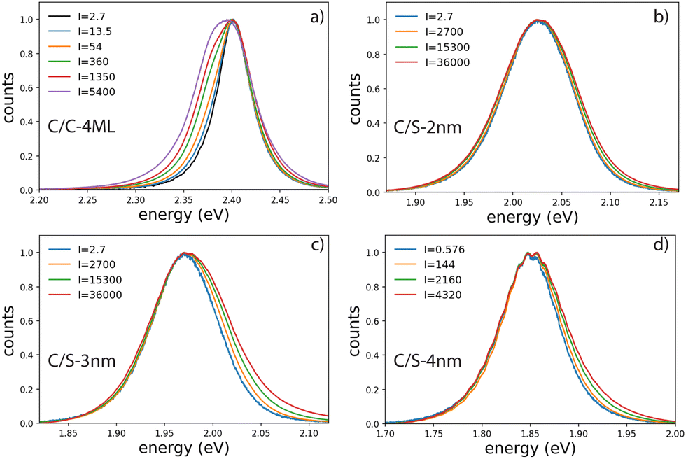 | ||
| Fig. 3 Evolution of the emission spectra at room temperature of the series of 4 NPLs having different shell thicknesses as a function of excitation intensity at 420 nm. The intensity is expressed in W cm−2. | ||
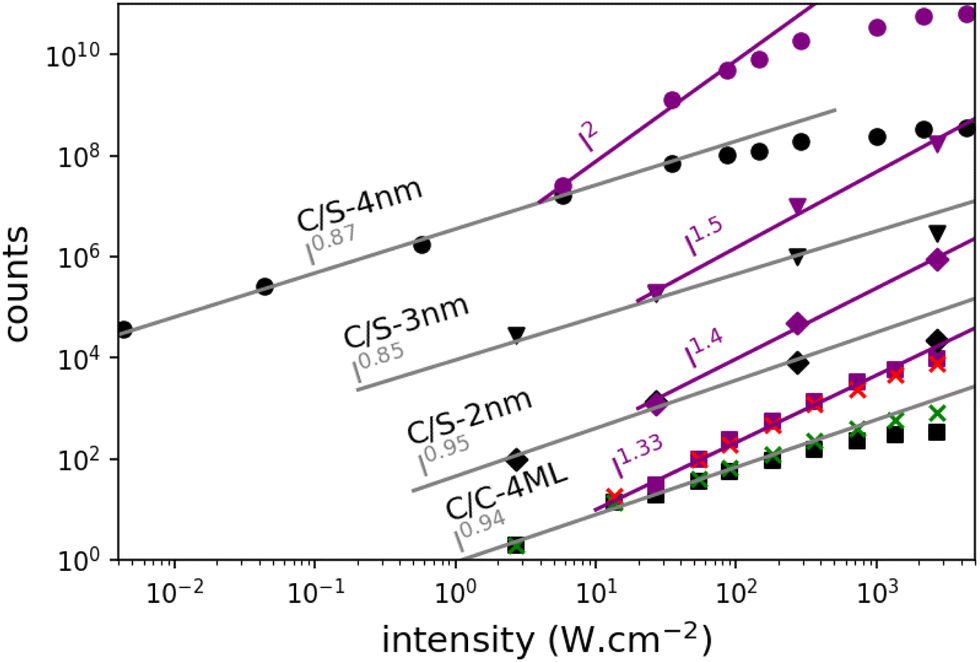
Emission spectra and decay times have been recorded simultaneously for intensities ranging from 10−3 W cm−2 to 4 × 10³ W cm−2. To avoid degradation, the sample was continuously scanned leading to irradiation times of less than 50 ms for a group of NPLs in the focal spot. The core–crown NPLs clearly demonstrate an additional emission peaking at about 20 meV on the low-energy side relative to the excitonic emission, with an increase in amplitude with the excitation intensity 3-a. As shown in the ESI† (Fig. SI-9), neither a Gaussian nor a Lorentzian function can properly fit the emission spectra recorded at the lowest excitation intensity, while a pseudo-Voigt profile is appropriate. When the excitation intensity is increased, 2 pseudo-Voigt functions are used, allowing to extract the first exciton position and a second contribution assigned as the bi-exciton contribution (XX). The obtained peak positions are stables for all fitted curves allowing to deduce a biexciton binding energy of 26 meV, in good agreement with the value obtained in ref. 25. The evolution of the signal as a function of the excitation intensity can also be deduced. Illustrative fittings are given in the ESI† (Fig. SI-8). The excitation intensity dependence of both bands can be plotted, and the red-shifted band demonstrates a power-law exponent of about 1.33 while the X0 emission follows an almost linear dependence (red and green crosses in Fig. 4). The power-law exponent smaller than 2 found for the bi-exciton reflects the Auger quenching occurring at high density of excitation.26
 | ||
| Fig. 4 Evolution of the X0 and XX intensities as a function of the power density of excitation at 410 nm. The curves have been multiplied by an adapted constant factor to obtain a clear figure. For the C/C-4ML NPLs, crosses correspond to the intensities deduced from emission spectra (green for X0 and red for XX). Black and purple scatters correspond to the intensities deduced from the decay times. The fast components (purple) exhibit a power law dependence with exponents over 1.3. The slow components (black) follow a power law with exponents about 0.9. | ||
The XX emission starts to be detectable for excitation intensities over 10 W cm−2. Yeltik et al. have measured the absorption cross-section of 4ML CdSe NPL at σ ∼ 5 × 10⁻¹⁴ cm2 at 400 nm.27 Considering our initial core area of 200 nm2 and the mean area of the final CC-NPs of about 800 nm2, we estimate the cross-section of our 4ML-CC NPL to be σ ∼ 20 × 10−14 cm2. We can deduce the mean number of electron–hole pairs created per excitation pulse and per NPL according to  , I, σ, Δt and E are the excitation intensity, the absorption cross section of a single NPL, the duration of the excitation laser pulse, and the excitation photon energy, respectively. The product I × σ therefore represents the total power absorbed by a single NPL per second. Multiplying it by the pulse duration gives the total energy absorbed by a single NPL per excitation pulse and finally, dividing this results by the energy of one excitation photon yields the number of absorbed photons per pulse per NPL. Considering our experimental parameters, XX can be observed for 〈N〉 larger than 0.14. The linear behavior of the monoexciton (X0) is observed from the lowest used intensity up to a 〈N〉 of about 3. The observed deviation from the linear behaviour may reflect a combination of saturation and degradation of the sample. The fluorescence decays have been measured simultaneously to the emission spectra and their evolution demonstrated, as expected, an acceleration when the intensity of excitation is increased (Fig. 5(a)). We can reasonably assign the fast contribution to XX (and all the charge declination) and the slow contribution to most probable excitons with linear behavior against intensity variations, i.e. X0, X− and X+, to the least. Considering the fast-component range (between 0 and 2 ns) and the range of the slower components between 15 and 30 ns, which are proportional to the XX and X0 emissions, respectively, we can deduce their respective evolution with the excitation intensity for C/C NPLs. Their intensities can then be plotted as a function of the excitation intensity as shown in Fig. 4 (purple and black squares), resulting in a very good agreement with similar curves deduced from two-peak fitting of the emission spectra (green and red crosses).
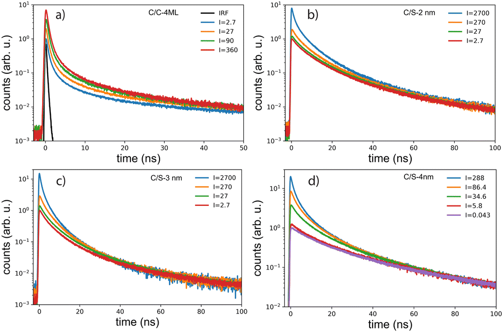 | ||
| Fig. 5 Evolution of the fluorescence decay at room temperature, as a function of the power density of excitation at 410 nm of the series of NPLs having different shell thicknesses. The power density is expressed in W cm−2. | ||
The case of the C/S NPLs is more complex to analyze. The C/S-2 nm NPLs only show a broadening of the emission spectrum when the intensity increases. Furthermore, this spectral change is observed at larger intensities as compared to C/C NPLs. The C/S NPLs with thicknesses of 3 and 4 nm show a blue-shifted broadening with increasing excitation intensity. For the 3 nm thick NPLs, a small broadening on the low energy side can be detected at high intensities. The fitting procedure with 2 pseudo-Voigt functions is less straightforward in this case and only spectra measured at high excitation intensities allow to extract two bands, while keeping the center position and the width deduced from the low-intensity spectra. Assigning the broadening and shoulders to the XX emission, the binding energy of the bi-exciton can be estimated as summarized in Table 2. Furthermore, one can then observe that even the addition of only a thin shell layer (about 0.4 nm on each side) switches the exciton–exciton interaction from attractive to repulsive. In order to estimate the excitation intensity dependence, the spectral evolution cannot be used with accuracy. We present in Fig. 5 illustrative fluorescence decay measurements for various excitation intensities for all samples (normalized at 50 ns for C/C-4ML, and 100 ns for C/S samples). Similarly to the C/C NPLS, the decay-time analysis is applied on the C/S-2, 3 and 4 nm to extract the power dependence of fast and slow components. The low-intensity decay time being longer than for the C/C-4ML NPLs, the slow component has been adapted between 30 and 40 ns for the C/S-2, and 3 nm, and between 60 and 80 ns for the C/S-4 nm. The intensity dependence is well described by a power-law function with exponents ranging from 0.9 to 1 for the slow component and between 1.4, 1.5 and 2 for the fast component of the C/S 2 nm, 3 nm and 4 nm respectively. This power-law dependence allows to assign the fast component to the XX emission and confirms that, despite a small spectral change observed for C/S-2 nm NPLs, the XX are indeed generated at high intensities of excitation. Only a weak broadening is observed without a shift, meaning that the bi-exciton binding energy is around 0 in this case. Note that the evolution of the shape of the decay curves differs from the C/C-4ML to the C/S NPLs. It appears to be the case that the value of the fast decay component is roughly independent of the excitation intensity for the C/C-4ML NPLs, while its relative amplitude increases significantly. On the other hand, the C/S-sample exhibits an acceleration of the fast decay when the excitation intensity is increased.
| E X0 (eV) | E XX (eV) | ΔEXX–X0 (meV) | |
|---|---|---|---|
| C/C-4ML | 2.404 | 2.378 | −26 |
| C/S-2 nm | 2.025 | 2.025 | 0 |
| C/S-3 nm | 1.971 | 2.025 | 17 |
| C/S-4 nm | 1.849 | 1.864 | 15 |
2.3 Comparing optical excitation and X-ray excitation
As they involve multiple time, energy and space scales, energy relaxation mechanisms under ionizing radiations differ significantly from those under optical excitation. The interaction of X-ray photons with materials leads to the photo-ionization of an electron from a deep band, generating a primary high-energy electron–hole pair composed of a deep hole and a hot electron (several keV). After a complex sequence of energy relaxation processes, secondary electrons and holes are forming excitons, leading to emission of light when radiative transitions are favorable. In the case of nanoparticles, for which the particle size is smaller than the mean migration distances of the involved species, the energy deposition and the distribution of excited states is extremely different from bulk materials: Nanocrystals experience significant escape of charges, depending on the particle size, as described in Bulin et al. and Meng et al.14,28 In the case of direct-bandgap semiconductors, the emission signatures of multi-excitons at the end of the relaxation process can be observed. Based on these analyses, we compared the excitonic species after the cascade of the secondary electrons under X-ray excitation and those generated by low intensity and high intensity optical excitation.As a first step towards probing the scintillation behavior in nanocrystals, we compared steady-state emission spectra under optical and X-ray excitation of the NPLs deposited on a silicon substrate (Fig. 6(a)).
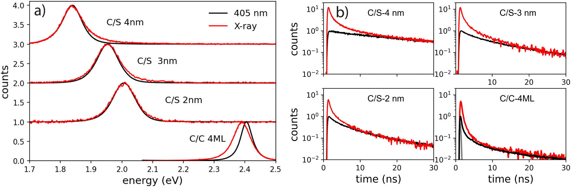 | ||
| Fig. 6 (a) Emission spectra and (b) fluorescence decay times at room temperature of the series of NPLs having different thicknesses ranging for C/C 4ML (1.2 nm), and C/S 2 nm, 3 nm and 4 nm under low power density of optical excitation (405 nm) and X-ray excitation. | ||
The photoluminescence (PL) spectra under weak intensity of optical pumping at 405 nm show a single symmetrical band attributed to X0 as already discussed above. On the exact same experimental set-up, the radioluminescence (RL) spectrum (X-ray excitation with 35 kV, 30 mA on the W anode), exhibits a behavior very similar to intense optical excitation, i.e. a red-shifted shoulder compared to low-intensity optical excitation for C/C NPLs, a weak broadening of the emission spectra for the C/S 2 nm, and a weak blue-shifted shoulder for the C/S 3 and 4 nm NPLs. For the C/S NPLs, this spectral comparison gives the impression that no XX are formed for the smallest thickness (2 nm), and that the probability to form XX increases when the thickness is larger (3 and 4 nm), which would be expected as discussed in the next section. One may nevertheless deduce from such a spectral comparison that C/C NPLs are more favorable to form XX. In light of the intense optical excitation as described above, the X0–X0 interaction energy of the bi-exciton has been estimated to be about 0 for the C/S 2 nm NPLs, and about +16 meV for the larger C/S NPLs, while it has been measured at −26 meV for the C/C NPLs. Combined with the larger FWHM of the X0 emission of the C/S samples, the XX emission is not less intense under X-ray excitation but less detectable by means of the radioluminescence spectroscopy. We have then compared the fluorescence decay times under low-power optical excitation and pulsed X-ray excitation (HV at 35 kV on the W anode). The amplitude of the X-ray excitation has been adapted to match the 30–50 ns domain of the 405 nm one (corresponding to the X0 emission) to highlight the extra fast emission under X-ray excitation, similarly to the intense optical excitation. The amplitude of the measured X-ray-induced decay time is then multiplied by about 12 for C/S 3 and 4 nm, by 6 times for the C/S 2 nm and 4 times for the C/C 4ML samples. The X-ray-induced decay analysis using the multi-components method and the 4 exponential fitting are presented in Fig. 7. For comparison, the results obtained under low-intensity optical excitation are also presented as dashed lines. The C/S samples clearly show extra bands at short times. In contrast, the structure of the decay decomposition is rather similar for the C/C NPLs, with an enhanced area of the short component and in consequence a reduced one for the slower component (>10 ns). Such behavior has been highlighted under intense optical excitation. The obtained parameters from the 4 exponent fitting are summarized in Table 1. Note that an extra very slow component appears the C/S 2 and 3 nm samples, probably reflecting trapping. On the other hand, this slow component can be hardly detected under X-ray for the C/C NPLs suggesting that the corresponding traps are not filled with X-ray excitation.
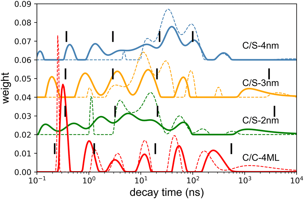 | ||
| Fig. 7 Solid line: decay-time distribution deduced from the multi-component fitting of the fluorescence decay time under X-ray excitation. Dashed line: for comparison, the same distribution for the 405 nm excitation. The black lines correspond to the decay times obtained using the 4 exponential fitting with maximum-likelihood estimation. | ||
2.4 Simulation of the energy relaxation
Detailed simulations using micro-theory of scintillation fully based on the dielectric response function of the material have been previously performed on SQWs to describe the formations of highly excited nanoparticles.14,29 As described above, X-ray irradiation at 35 keV produces fast primary electrons with kinetic energies from 10 to 35 keV. The absorption of an X-ray photon can occur in any nanoparticle or in the substrate, and the primary photoelectron produces secondary electronic excitations (SE) in different NPLs along the path of the fast electron. The number of scattering events with production of secondary electron–hole pairs can be estimated as stopping power (−dE/dx) for electrons with energies of 1 to 35 keV, multiplied by the length of the electron trajectory traversing the NPL and divided by the plasmon energy, which corresponds to the maximum of the energy-loss function (about 12 eV for CdS and CdSe). The value of the stopping power is about the same for all materials that form the NPLs. The mean number of the SE produced in an NPL depends thus on the distribution of in-particle trajectory lengths and Poisson statistical factors. The length of the photoelectron trajectory depends also on the angle between the normal to the NPL plane and photoelectron trajectory, and most of these lengths are about the thickness of the NPL since a small fraction passes the NPL with a direction parallel to the NPL plane. Therefore a large fraction of photoelectrons do not produce SE in thin NPLs (see Fig. 8(a)), and the distribution of the numbers of scattering processes depends weakly on lateral size (see Fig. 8(b)). For a 30 nm diameter NPL and for thicknesses of 1, 2, 3 and 4 nm, the fraction of multiscattering (likely to generate XX) to single scattering are estimated to be 36%, 42%, 47% and 48% respectively and the non-interacting fraction decreases from 72% to 39%. These rough estimates show that the contribution of XX emission is expected to increase by about 30% from 1 to 4 nm. Secondary excitations with energies close to the plasmon energy relax within the NPL under production of a few low-energy electron–hole pairs, the final number of which is also controlled by Auger processes with hot electrons and holes as described in ref. 14). The number of low-energy electron–hole pairs in the NPL is proportional to the number of primary scattering processes. After thermalization, these electron–hole pairs can form excitons. If more than two excitons are formed in one NPL, they can be combined into biexcitons with corresponding modification of emission and decay rates. As shown previously, the formation of XX depends on the presence of the shell, whose thickness as shown in Table 2. As speculated in Fig. 2(b), the band alignment is supposed to lead to quasi-type II C/S NPLs where electrons and holes wavefunctions expand in different ways in the shell and the one-dimensional confinement thus differs for electrons and holes. Note that in the case of type I core/shell NPLs, the situation is supposed to be similar to core–crown NPLs and a red shift of the XX emission is observed as demonstrated in ref. 17 and 30. Differences in the shell gradient composition (Cd/Zn ratio) may explain this type I or quasi type II behavior. The hole wavefunction spreads only over the core thickness (about 1 nm), whereas the electron wavefunction extends over the whole thickness of the NPL because of the small difference in energy of the bottoms of the conduction-bands of CdSe and CdZnS. For thick NPLs (>3 nm) the spread of electron wavefunction is limited by the free-exciton radius (about 2.5 nm). Therefore, for C/C (or type I C/S), electrons and holes have about the same distribution over the thickness (Fig. 8(d)) and the lateral charge distributions for the electron and the hole are the same.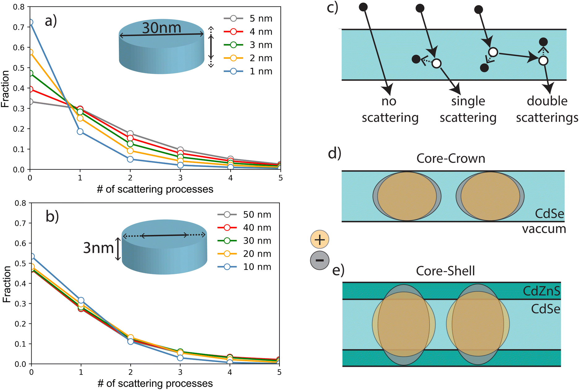 | ||
| Fig. 8 (a) Distribution of the number of scattering processes in CdSe NPLs when varying the thickness (a), and the lateral size (b). (c) Example of situation with 0, 1 and 2 scattering processes. Schematic charge distribution of holes and electrons in the case of core–crown (d) and core–shell NPLs (e). | ||
In the case of optical excitation, a four-particle system as described in ref. 25 is formed directly and accounting for multiple mirror image charges. Ionizing radiation, on the other hand, generates free charges which may recombine into excitons and potentially into bi-excitons, i.e. the same species as obtained under optical excitation. The scintillation process thus induces an intermediate stage of interaction between two excitons which have not yet formed a four-particle biexciton. In this case the excitons are considered as two distinct entities interacting through direct Coulomb coupling of two quadrupoles, as well as due to polarization of one exciton by charge fluctuations in the other exciton (similar to the case of two neutral atoms). The latter interaction results in attractive dipole–dipole forces, and for objects with complicated geometries the interaction energy could even deviate from the usual r−6 power law, leading to potentially bound or anti bound energy levels. The attraction of two excitons means that the energy of the bi-exciton is lower than the energy of two individual excitons (2Eex − Ebibound). After the recombination of one e–h pair in the process “bi-exciton → exciton + photon” one of the excitons remains, and therefore the energy of emitted photon equals Eex − Ebibound, which results in a red shift. In case of repulsive excitons, no bi-excitons can be created in infinite crystal. Nevertheless, in systems with quantum confinement two excitons can coexist at the distances less than the lateral size of the NPL. Therefore their energy is larger than twice the energy of a single exciton in the same NPL, and the photon emitted after recombination has a blue-shifted wavelength. The size of this blue shift should be weaker since the distance between repulsive excitons is determined by the lateral size, whereas for attractive excitons the distance between two excitons is about exciton radius which is smaller than NPL size (in most cases the attractive exciton forms a cluster of two electrons and two holes in which we cannot even distinguish two excitons).
In C/C or type I C/S NPLs, dipolar interaction is dominating and a red shift of the XX emission is observed. When the thickness is increased as obtained in quasi-type II C/S NPLs, the distribution of the charges uniformity is broken and forms a negative–positive–negative distribution across the NPL thickness. The quadrupole moment increases with the growing spread of the electron wavefunction. The experimental estimation of XX energies presented above shows that for 2 nm C/S, Coulomb repulsion of two excitons almost compensates dipolar attraction, and the XX has no additional binding energy. The spread of electron wavefunction is higher in 3 and 4 nm C/S NPLs, and about the same for these two thicknesses since the exciton radius is of the same order of magnitude as or less than the NPL thickness. Therefore two excitons repulse each other as illustrated by the observed blue-shift of the emission. This different behavior of two excitons shows that XX state can be easily produced when two separate excitons are formed under X-ray excitation in C/C NPLs due to their attraction. On the contrary, two excitons in thick C/S NPLs repulse each other and can be separated along the lateral dimension.
3 Conclusions
To summarize, we have synthesized a series of core/crown and core–shell NPLs of CdSe/CdS and CdSe/CdZnS compositions, with thicknesses ranging from 1.2 nm to 4 nm and exhibiting high luminescence quantum yields. Through the analysis of time-resolved dynamics and spectra under intense optical excitation, we demonstrate that the exciton–exciton interaction shifts from the attractive to repulsive regime when the thickness is increased. We deduce that a shell layer of 0.4 nm is enough to break the “neutral” character of the exciton responsible for the attractive van der Waals interaction leading to the red-shifted emission of the XX in the case of the C/C NPLs. We highlight the multiexciton generation under X-ray excitation in these 2D heterostructural NPLs, and estimate the expected number of electron multi-scattering compared to single-electron scattering probabilities as a function of thickness. Contrary to the core/crown heterostructure, the fast multi-exciton emission is blue shifted as soon as a shell of 0.4 nm is deposited. Despite larger thicknesses being more favourable for X-ray and γ-ray absorption, as well as for multi-exciton generation, the strategy of shell covering is not adapted to address the self-absorption issue, in addition to the slower response observed. In this family of compounds, the 2D core–crown nanoplatelets remain the best choice, combining ultra fast decay and a red shifted bi-exciton, despite being more prone to Auger quenching and exhibiting surface defects. Our study provides a direct insight to 2D NCs-based fast scintillation materials, beneficial to the selectivity and development of nano-scintillators.Conflicts of interest
There are no conflicts to declare.Acknowledgements
The authors thank for the financial support from China Scholarship Council. The research has been developed in the frame of the Crystal Clear Collaboration.Notes and references
- S. Ithurria and B. Dubertret, J. Am. Chem. Soc., 2008, 130, 16504–16505 CrossRef CAS PubMed.
- S. Ithurria, M. D. Tessier, B. Mahler, R. P. S. M. Lobo, B. Dubertret and A. L. Efros, Nat. Mater., 2011, 10, 936–941 CrossRef CAS PubMed.
- Y. Kelestemur, Y. Shynkarenko, M. Anni, S. Yakunin, M. L. De Giorgi and M. V. Kovalenko, ACS Nano, 2019, 13, 13899–13909 CrossRef CAS.
- N. Taghipour, S. Delikanli, S. Shendre, M. Sak, M. Li, F. Isik, I. Tanriover, B. Guzelturk, T. C. Sum and H. V. Demir, Nat. Commun., 2020, 11, 3305 CrossRef CAS PubMed.
- B. Liu, Y. Altintas, L. Wang, S. Shendre, M. Sharma, H. Sun, E. Mutlugun and H. V. Demir, Adv. Mater., 2020, 32, 1905824 CrossRef CAS PubMed.
- M. Sharma, K. Gungor, A. Yeltik, M. Olutas, B. Guzelturk, Y. Kelestemur, T. Erdem, S. Delikanli, J. R. McBride and H. V. Demir, Adv. Mater., 2017, 29, 1700821 CrossRef PubMed.
- R. Turtos, S. Gundacker, A. Polovitsyn, S. Christodoulou, M. Salomoni, E. Auffray, I. Moreels, P. Lecoq and J. Grim, J. Instrum., 2016, 11, P10015 CrossRef.
- J. Q. Grim, S. Christodoulou, F. Di Stasio, R. Krahne, R. Cingolani, L. Manna and I. Moreels, Nat. Nanotechnol., 2014, 9, 891–895 CrossRef CAS PubMed.
- C. Dujardin, E. Auffray, E. Bourret-Courchesne, P. Dorenbos, P. Lecoq, M. Nikl, A. VasilEv, A. Yoshikawa and R.-Y. Zhu, IEEE Trans. Nucl. Sci., 2018, 65, 1977–1997 CAS.
- M. Nikl, Meas. Sci. Technol., 2006, 17, R37 CrossRef CAS.
- R. Turtos, S. Gundacker, S. Omelkov, B. Mahler, A. Khan, J. Saaring, Z. Meng, A. Vasilev, C. Dujardin and M. Kirm, et al. , npj 2D Mater. Appl., 2019, 3, 1–10 CrossRef CAS.
- Y. Kelestemur, B. Guzelturk, O. Erdem, M. Olutas, K. Gungor and H. V. Demir, Adv. Funct. Mater., 2016, 26, 3570–3579 CrossRef CAS.
- L. A. Padilha, W. K. Bae, V. I. Klimov, J. M. Pietryga and R. D. Schaller, Nano Lett., 2013, 13, 925–932 CrossRef CAS PubMed.
- Z. Meng, B. Mahler, J. Houel, F. Kulzer, G. Ledoux, A. Vasil’ev and C. Dujardin, Nanoscale, 2021, 13, 19578–19586 RSC.
- W. K. Bae, L. A. Padilha, Y.-S. Park, H. McDaniel, I. Robel, J. M. Pietryga and V. I. Klimov, ACS Nano, 2013, 7, 3411–3419 CrossRef CAS PubMed.
- A. Schlosser, R. T. Graf and N. C. Bigall, Nanoscale Adv., 2020, 2, 4604–4614 RSC.
- Y. Altintas, K. Gungor, Y. Gao, M. Sak, U. Quliyeva, G. Bappi, E. Mutlugun, E. H. Sargent and H. V. Demir, ACS Nano, 2019, 13, 10662–10670 CrossRef CAS PubMed.
- R. Benchamekh, N. A. Gippius, J. Even, M. O. Nestoklon, J.-M. Jancu, S. Ithurria, B. Dubertret, A. L. Efros and P. Voisin, Phys. Rev. B, 2014, 89, 035307 CrossRef.
- J. Cui, A. P. Beyler, I. Coropceanu, L. Cleary, T. R. Avila, Y. Chen, J. M. Cordero, S. L. Heathcote, D. K. Harris, O. Chen, J. Cao and M. G. Bawendi, Nano Lett., 2016, 16, 289–296 CrossRef CAS PubMed.
- L. T. Kunneman, J. M. Schins, S. Pedetti, H. Heuclin, F. C. Grozema, A. J. Houtepen, B. Dubertret and L. D. A. Siebbeles, Nano Lett., 2014, 14, 7039–7045 CrossRef CAS PubMed.
- M. D. Tessier, B. Mahler, B. Nadal, H. Heuclin, S. Pedetti and B. Dubertret, Nano Lett., 2013, 13, 3321–3328 CrossRef CAS PubMed.
- S. O. M. Hinterding, B. B. V. Salzmann, S. J. W. Vonk, D. Vanmaekelbergh, B. M. Weckhuysen, E. M. Hutter and F. T. Rabouw, ACS Nano, 2021, 15, 7216–7225 CrossRef CAS PubMed.
- Z. Wen, P. Liu, J. Ma, S. Jia, X. Xiao, S. Ding, H. Tang, H. Yang, C. Zhang, X. Qu, B. Xu, K. Wang, K. L. Teo and X. W. Sun, Adv. Electron. Mater., 2021, 7, 2000965 CrossRef CAS.
- X. Jin, K. Xie, T. Zhang, H. Lian, Z. Zhang, B. Xu, D. Li and Q. Li, Chem. Commun., 2020, 56, 6130–6133 RSC.
- D. Macias-Pinilla, J. Planelles and J. I. Climente, Nanoscale, 2022, 14, 8493–8500 RSC.
- E. Baghani, S. K. O’Leary, I. Fedin, D. V. Talapin and M. Pelton, J. Phys. Chem. Lett., 2015, 6, 1032–1036 CrossRef CAS PubMed.
- A. Yeltik, S. Delikanli, M. Olutas, Y. Kelestemur, B. Guzelturk and H. V. Demir, J. Phys. Chem. C, 2015, 119, 26768–26775 CrossRef CAS.
- A.-L. Bulin, A. Vasil’ev, A. Belsky, D. Amans, G. Ledoux and C. Dujardin, Nanoscale, 2015, 7, 5744–5751 RSC.
- A. N. Vasil’ev, Microtheory of Scintillation in Crystalline Materials, Springer International Publishing, 2017, pp. 3–34 Search PubMed.
- Y. Altintas, U. Quliyeva, K. Gungor, O. Erdem, Y. Kelestemur, E. Mutlugun, M. V. Kovalenko and H. V. Demir, Small, 2019, 15, 1804854 CrossRef PubMed.
Footnote |
| † Electronic supplementary information (ESI) available. See DOI: https://doi.org/10.1039/d2ma00635a |
| This journal is © The Royal Society of Chemistry 2022 |