Electron–phonon interaction and ultrafast photoemission from doped monolayer MoS2
Neha
Nayyar
,
Duy
Le
 ,
Volodymyr
Turkowski
and
Talat S.
Rahman
 *
*
Department of Physics, University of Central Florida, Orlando, FL 32816, USA. E-mail: talat.rahman@ucf.edu
First published on 13th October 2022
Abstract
We have examined the effect of electron–phonon coupling on photoluminescence and ultrafast response of electron doped monolayer MoS2, using a combination of density functional theory, time dependent density functional theory, and many-body theory. For small doping (∼1–3%) of interest here, the electron–phonon coupling parameter is modest (∼0.1–0.2) but its effect on the emissive properties and response of the system to femtosecond (fs) laser pulses is striking. We find an ultrafast (fs) relaxation of the electronic subsystem as well as a high fluence of visible light emission induced by electron phonon interaction. Together with high carrier mobility, these features of monolayer MoS2 may be relevant for optoelectronic technologies.
I. Introduction
Several properties of single-layer MoS2 make it attractive for novel applications in nanoelectronics1,2 and nanooptics.3,4 Its high electron mobility, room-temperature current on/off ratio and ultralow standby power dissipation make it suitable for field-effect transistors.5 Optical pumping with circularly polarized light which leads to complete (nanosecond-long) dynamic valley polarization5,6 invites applications. Furthermore, its tuneable electronic structure and strong absorption and emission could be relevant for phototransistors7 and light emitting devices operating in the visible region.8 Of course, what has highlighted monolayer MoS2 is its enhanced luminescence, which is several orders of magnitude larger than that of its bulk counterpart.9,10 This increase in photoluminescence (PL) intensity of the monolayer has been attributed to its direct band gap. Experimental groups have reported the energy of the PL peak to lie in the range 1.8–1.9 eV, depending on the sample used.9–14The absorption spectrum of single layer MoS2 appears also attractive from the technological point of view, since the optical gap lies in the visible (∼1.8 eV) and the spectrum demonstrates peaks that correspond to strongly bound excitons9 and trions15 with experimentally observed large binding energies of ∼0.2–0.4 eV9,10,12 and 20 meV,15 respectively, making these states suitable for room-temperature applications. Theoretical studies of excitons using the phenomenological Wannier equation, as well as many body GW/Bethe–Salpeter equation (GW/BSE) approaches16,17 reproduce the large binding energies, while a trial wave function method does so for both the exciton and the trion bound states.18 Using a density matrix based time-dependent density functional theory (TDDFT) approach which is suitable for calculating properties of both excitons and trions19 we also confirm that the binding energies of these quasiparticles are much larger than what is expected in a typical semiconductor (few meVs). These large binding energies indicate the propensity of the excitons and trions to survive at temperatures at which phonons effects are enhanced and electron–phonon interactions impact the absorption and emission spectra, which is part of the motivation for this work.
Another motivation for the present study comes from the recent interesting experimental observations of strong emission in the ultrafast optical response,20 which stimulated measurements of its ultrafast electron response,21–23 followed by that of time-resolved femtosecond emission24,25 of a related two dimensional material, graphene. Theoretical analyses26–28 confirm the main experimental conclusion that the ultrafast electron response leads to an ultrafast emission, with dominant electron–phonon scattering of hot electrons.26 Remarkable carrier multiplication and Auger recombination were also predicted for excited states of graphene.27,28 Given its strong absorptive and emissive properties, it is natural to expect similar phenomena in excited states of monolayer MoS2. Indeed, PL spectra and nonequilibrium response of the latter are topics of active experimental studies.29–47 Note that the PL spectrum is dominated by exciton peaks.34,35 For instance, the spectrum includes one sharp PL peak at 640 nm and one broad peak at 684 nm corresponding to the excitonic A (1.94 eV) and B (1.81 eV) direct-gap optical transitions, respectively.35 Regarding PL energies, it is important to bear in mind that there is a possibility of (strong) ultrafast gap renormalization caused by the presence of excited carriers, as recent time-resolved and angle-resolved photoemission (TR-ARPES) data demonstrate.36 Moreover, combined experimental PL and theoretical analysis showed37 there are two possible distinct channels of excitations in monolayer (1L) MoS2: an excitation above the band gap and quasi-resonant excitonic states below the band gap, with a much stronger (excitonic) emission in the former channel (see also a review,38 in which details of exciton emission and gap renormalization in excited 1L MoS2 are discussed).
Furthermore, ultrafast time-resolved photoemission experiments at low temperatures on 1L MoS2 flakes29 show photocarrier recombination to occur on a few-picosecond timescale, while a biexponential PL decay was observed when the temperature was increased. In femtosecond pump–probe pulse studies on few-monolayer MoS2,30 the carrier lifetime was estimated to be ∼100 ps. Optical pump–probe spectroscopic studies31,32 suggest that carrier cooling (dominated by phonon scattering) occurs on the picosecond scale, with 500 fs electron thermalization, followed by 1–100 ps31 defect-caused transient processes, and by slower, ∼10 ns, recombination.32 On the other hand, there are experimental indications of an ultrafast response in the system: PL mapping pump–probe spectroscopy measurements reveal a 50 fs hole transfer from MoS2 to WS2 layer in photoexcited atomically thin MoS2/WS2 heterostructure.33 Theoretical modelling predicts a 100 fs phonon lifetime resulting from electron–phonon scattering.48
Importantly, time-resolved PL data39 show a decrease of the initial polarization (exciton emission decay time ∼4 ps) in 1L MoS2 with increasing pump photon energy suggesting ultrafast intervalley relaxation. The above observations are supported by TR-PES and ARPES measurements for 1L MoS2 on a metallic substrate40 which demonstrate ultrafast (50 fs) extraction of excited free carriers via the metal, suggesting ∼50 fs dynamics of the gap change. Similarly, fs-timescale for the PL decay of excitons in the system has been reported.41 Thus, there are several evidence of the ultrafast fs dynamics of free charges and excitons in 1L MoS2. As we show in this work, electron–phonon interaction also plays as important role in the ultrafast dynamics of the system.
There are also interesting observations on 1L MoS2 on the effect of the time-dependent electronic temperature on the emission42,43 and fluence.43–47 For example, femtosecond pump–probe spectroscopy found that electron–phonon scattering is responsible for an ultrafast redshift of the exciton resonance energy observed after photoexcitation.42 The energy from the cooling of hot carriers and from the formation of bound states is transferred to the phonon subsystem within 2 ps, though some sub-ps emission dynamics was also observed. Electron temperature-change and fluence dependent studies43 imply that the dissociation of excitons leads to an observed ultrafast bandgap renormalization. Analysis of exciton generation and dynamics at different pump fluences found that both ultrafast phenomena strongly depend on fluence.44 Similarly, observed 100 fs dynamics of excited free carriers in 1L MoS2 also depends strongly on pumped fluence.46,47
The results mentioned above are intriguing and call for a microscopic understanding of the ultrafast response and PL of monolayer MoS2. Such a theoretical analysis needs to consider electron–phonon scattering processes, which may define the dispersion and the lifetime of excited electrons and, hence, the PL of the system. In this work, we first calculate electron–phonon interaction in 1L MoS2 at small values of doping (∼1–3%) which we introduce by shifting the chemical potential to the conduction band. This process is akin to the application of an external voltage to the system. We then examine effects of electron–phonon interaction on the absorption and emission properties of this remarkable 2D material. In Section II, we present some details of the calculations of the electron–phonon coupling, which is followed in Section III by an analysis of the absorption and emission properties. The ultrafast response of the system is summarized in Section IV and our conclusions are presented in Section V.
II. Electron–phonon coupling in doped 1L MoS2
To calculate electron–phonon interaction one needs to first obtain the electronic structure of the material (electron density of states) and its phonon dispersion curves. Although the electronic structure of the ground state of monolayer MoS2 has been calculated by a number of researchers, for completeness and consistency we present here results of our calculations for which we have applied the density functional theory (DFT) based approach as embodied in the code Quantum Espresso.49 The model system consists of two planes of hexagonally arranged S atoms covalently bonded to the layer of Mo atoms sandwiched between the S layers (Fig. 1). The lattice parameter was obtained through ionic relaxation of the system within the Local Density Approximation (LDA) for the exchange–correlation potential, using an energy cut-off of 60 Ry for the plane-waves and a 15 × 15 × 1 k-point mesh for sampling of the Brillouin zone (with Gaussian smearing with σ = 0.004 Ry for integration over the Brillouin zone). To avoid effects of the interaction between images in the periodic unit cell, the lattice parameter in the direction perpendicular to the monolayer plane was chosen to be 15 Å (vacuum layer). The calculations yielded a lattice parameter of 3.167 Å and Mo–S bond length of 2.419 Å, in reasonable agreement with experimental values 3.15 Å and 2.414 Å, respectively.50,51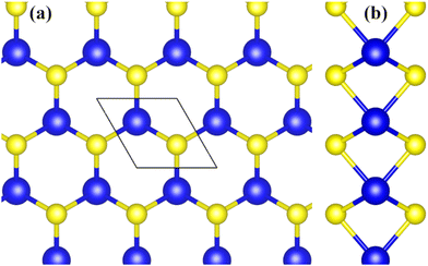 | ||
| Fig. 1 Top view (a) and side view (b) of monolayer MoS2. Blue and yellow balls represent Mo and S atoms, respectively. The parallelogram in (a) indicate a unit cell of MoS2. | ||
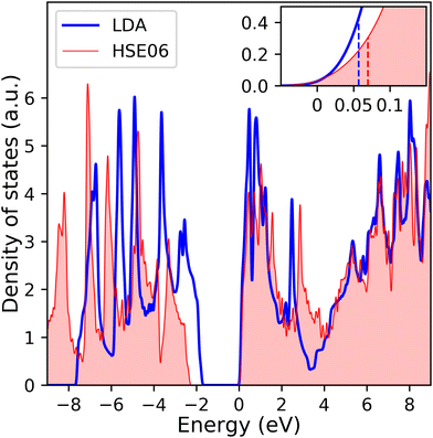
The calculated electronic density of states (DOS) of the system, shown in Fig. 2, has a band gap of 1.8 eV in agreement with prior DFT-LDA calculations,52,53 though it is smaller than the experimental value of 2.15 eV.54 The theoretical value of the gap increases when taking into account the GW correction (though that leads to an overestimation as the gap is found to be ∼2.8 eV55). On the other hand, the gap in the optical absorption spectrum (from excitonic effects) is about 1.8 eV. This good agreement between the DFT electronic gap and experimental optical gap is fortuitous and reflects the large excitonic binding energies, ∼0.2–0.4 eV (see ref. 19 and references therein). These large binding energies are caused in part by reduced screening of the electron-hole attraction in these two-dimensional systems. Another consequence of the reduced screening is a rather long (up to 1000 ps) exciton lifetime56,57 and a small (7–10 Å) exciton radius.58
To validate our DFT-LDA results, we repeated the calculation of the electronic density of states of 1L MoS2 with the more computationally intensive Heyd–Scuseria–Ernzerhof (HSE06) hybrid functional.59,60 These hybrid functionals incorporate the short range Hartree–Fock exchange interactions and typically provide band gap for transition metal dichalcogenides that are in better agreement with experimental values.61 Comparison of the electronic DOS obtained with LDA and HSE06 in Fig. 2 highlight two points. First, the band gap (∼2.2 eV) is in excellent agreement with experimental values. Second, despite differences in the DOS, the bottom of conduction band, which is the main quantity of interest here (see below), is virtually the same, whether calculated with LDA or HSE06. We have further elaborated the region near the Fermi energy in the inset in Fig. 2 to point to the quantitative differences in N(εF) that the two methods yield. For small doping (1–3%, i.e., 0.01–0.03 electron per formula unit), the differences are within the margin of error that is introduced by the smearing that is necessary for calculations of the DOS. Given the computational efficiency of LDA, and our interest is understanding the trends in the behavior of the electron–phonon interaction, we will proceed with LDA for the rest of this study, since we expect the trends to be the same (our rationale is similar to that used in ref. 61). Before we discuss the effects of the excitons on the optical spectra of undoped and doped monolayer MoS2, we turn to the description of the phonon dispersion curves of the undoped system.
Fig. 3a shows the phonon energy dispersion curves. The system has the symmetry of point group D3h. There are 9 branches of phonons, corresponding to 3 acoustic and 6 optical modes. The acoustic modes labelled LA and TA, in Fig. 3, are in-plane vibrations that have linear dispersion and have higher energy than the acoustic mode labelled ZA which consists of out-of-plane vibrations. The lowest-energy optical modes E′ and E′′ consists of in-plane vibrations, shown schematically in Fig. 3b, both being degenerate at the Γ-point. The two E′′ modes are vibrations with 2 sulphur atoms moving out-of-phase while keeping the Mo atom static. The two E′ modes are polar modes with Mo and S atoms moving out-of-phase with respect to each other. A′ is a homopolar mode with two sulphur atoms vibrating out-of-phase while the Mo atoms remain static, and A′′ is the highest energy optical mode with out-of-plane vibrations in which the Mo and S atoms vibrate out-of-phase with respect to each other.
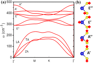 | ||
| Fig. 3 Phonon dispersion curves (a) and schematic representation of the optical phonon modes (b) for monolayer MoS2 obtained from DFT calculations. | ||
The calculated phonon dispersion curves of monolayer MoS2 presented in Fig. 3 are in agreement with experimental Raman spectra for the optical modes frequencies at the Γ-point62–66 (∼385 cm−1 for the E12g and 400–410 cm−1 for the A1g mode), as well as with other DFT calculations.67–71
To calculate the electron–phonon coupling parameter we have applied the Quantum Espresso post-processing software, which uses the results for the ground state atomic and electronic configurations, wave functions and phonon dispersion curves to obtain the electron scattering probability coefficients
 | (1) |
![[small epsilon, Greek, circumflex]](https://www.rsc.org/images/entities/i_char_e107.gif) qν (for a summary on the Eliashberg formalism to study the effects of the electron–phonon interaction used in this work, see, e.g., ref. 72).
qν (for a summary on the Eliashberg formalism to study the effects of the electron–phonon interaction used in this work, see, e.g., ref. 72).
Next, from the above scattering function one can obtain the phonon line widths:
 | (2) |
 | (3) |
 | (4) |
 | (5) |
| Doping (%) | λ |
|---|---|
| 1 | 0.12 |
| 2 | 0.16 |
| 3 | 0.20 |
Our results are also in agreement with those obtained Ge and Liu74 for similar doping. For reasons discussed by Ge and Liu74 there is a dramatic increase in λ when doping is larger than 5%. Such large values of λ(∼1) have been extracted from the temperature dependence of the helium-atom scattering (HAS) Debye–Waller factor75 in range 100–500 K. Since Anemone et al.75 have discussed their findings within the context of our results above (which had been posted in the archives76) and those in ref. 75, there is no inconsistency in the divergent values of λ that have been reported. For small doping (<5%) the electron phonon coupling parameter in 1L MoS2 lies between 0.1 and 0.2. In the section below we use the values of λ from Table 1 to study the optical properties of the system.
III. The absorption and the emission spectra
To study the absorption and emission properties, we calculate the momentum-resolved spectral function A(k,ω) (proportional to the probability for an electron to occupy the state with energy ħω and momentum k): | (6) |
 | (7) |
 | (8) |
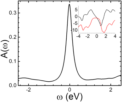
A typical plot of the spectral function, calculated using eqn (6) at 1%-doping, is presented in Fig. 4 (following the results for the phonon spectrum in Fig. 3, we have chosen ωmax = 0.0497 eV which is the (optical) phonon frequency). In the insert of Fig. 4 we show the corresponding frequency dependencies of the real and imaginary parts of the electron self-energy. The values of the imaginary part of Σ at low frequencies (∼1 eV) suggest that one needs to consider femtosecond processes (scattering times ∼1/ImΣ) to properly describe ultrafast dynamics in doped 1L MoS2. It must be noted that the carrier lifetimes 1–100 ps, reported in the literature29–32 for the undoped excited system is most probably related to exciton recombination times, which can be ascribed to various processes (for example, charge or defect scattering). The doped system may demonstrate dynamics faster than the above because of enhanced electron–phonon interaction, as we show in the following section.
Another pronounced feature in the electron self-energy in Fig. 4 is the suppression of the imaginary part of Σ at frequencies in the range of those of the phonons (<100 meV) see red curve in the inset), because of electron–phonon scattering processes. Also note the peaks in the real part of the self-energy at higher frequencies on both sides of the Fermi level (around +0.91 eV and −1.27 eV in the inset in Fig. 4), indicating enhanced electron–phonon scattering processes. Interestingly, similar frequency-dependence of the real and imaginary part of the self-energy was predicted for graphene which resulted in a kink in the electronic spectrum at frequencies close that of the optical phonon (Einstein model).77
The absorption and emission spectra of the undoped system are presented in Fig. 5. The absorption spectrum (inset in Fig. 5) was calculated by including excitonic states within the density-matrix TDDFT approach78 with the Slater exchange–correlation kernel (see ref. 19 for calculational details). The absorption spectrum shows two prominent features – one corresponding to excitonic transition (binding energy ∼1.0 eV) and the other to interband (valence-conduction) excitations (only the lowest conduction band has been considered). The shape of the spectrum is in reasonable agreement with experimental data.35,37,38 However, we needed to shift the spectrum to the right by 1 eV to align it close to experimental data (see above). The inset in Fig. 5 does not display the B exciton, which is a limitation of the Slater exchange–correlation kernel that we have used in the TDDFT calculations. It must be noted that position of the exciton peak depends in general on temperature,38 depiction of which requires combining TDDFT with many-body phonon approaches that are beyond the scope of this work.
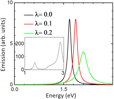 | ||
| Fig. 5 The emission spectrum of monolayer MoS2 at different values of λ. Inset: The corresponding absorption spectrum at λ = 0. | ||
We now turn to the emission spectrum in Fig. 5 which is obtained from the absorption spectrum after inclusion of the phonon correction to the electron self-energy obtained from eqn (7). The effect of the electron–phonon coupling parameter on the PL peak position is amply clear from Fig. 5: the peak moves to higher energies with increasing λ. As expected the linewidth also increases with increasing λ. The position of the PL peaks for all three values of λ lies in the range seen in experiments29,30 (again, with renormalization of the bandgap).
IV. Ultrafast response of doped system
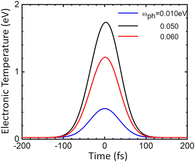
Finally, we present a simple analysis of the ultrafast response of the system to an external laser perturbation. As mentioned in the Introduction, ultrafast experimental studies of undoped MoS2 systems (flakes,29 few-monolayer,30 multilayer,31 monolayer32) reveal picosecond response, with the general conclusion that most probably this timescale is defined by the exciton recombination time. Indication of faster processes were found in experiments of Hong et al.33 who report 50 fs hole transfer time from a MoS2 to WS2 layer of the corresponding heterostructure, and in theoretical works of Kaasbjerg et al.,48 who predicted phonon lifetime of 100 fs in monolayer MoS2. On the other hand, there is very little information on the ultrafast response of doped MoS2, which would be interesting given the intriguing results already obtained for graphene. Note that the femtosecond response in doped graphene20 demonstrated that the electron relaxation takes place in tens of femtoseconds, with a similar scale for the consequent irradiance times. Since the electron–phonon coupling parameter and several other characteristics of graphene and monolayer MoS2 are similar, and the emissivity (undoped case) is even stronger for MoS2, one might expect pronounced emission and other ultrafast processes in the later as well.To explore such a possibility, we begin by establishing the timescales of the dynamics of the system when probed by ultrafast pulses. For this, we consider the equilibration (thermalization) of the electronic subsystem because of electron- phonon scattering using the Allen approximation,79 in which the equation for the time dependence of the electronic temperature Te has the following form:
 | (9) |
 | (10) |
Since the time of relaxation of the electronic subsystem from Te to room temperature TL defines the timescale for equilibration of the whole system, i.e., the time for all emission processes, one can expect the phonon-stimulated radiation to also occur in the femtosecond regime. We thus analysed the energy dependence of the spectral fluence of the system (the total radiant energy emitted in all directions per unit area per photon energy) using the Planck formula:
 | (11) |
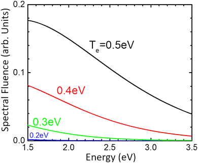 | ||
| Fig. 7 The spectral fluence of doped monolayer MoS2 at different electronic temperature. The values for other parameters are given in the text. | ||
These results along with experimentally observed high electron mobility suggest rich ultrafast dynamics of the doped MoS2, with possible practical ultrafast applications. Several interesting phenomena may exist, such as carrier multiplication27 and Auger recombination28 that have been predicted for graphene. The unique characteristics of MoS2 may suggest some other effects, the first of which is the pronounced emissivity.
V. Conclusions
To summarize, we have studied the effects of the electron–phonon coupling on the optical response of pure and doped monolayer MoS2, including its ultrafast response. The absorption spectrum of the undoped system demonstrates an excitonic peak in the visible range, in agreement with experimental data. The position of the emission peak is sensitive to the value of electron–phonon coupling, but for the doping levels considered here it lies in the visible and in the experimentally observed range 1.8–1.9 eV. Our calculated electron–phonon coupling constant are of order (or even larger than) the one obtained theoretically for doped graphene.77,80 This suggests that one may expect ultrafast response of monolayer MoS2 caused by thermalization effects to be similar to graphene.20 Indeed, the results for the electron self-energy of the doped systems gives estimated lifetimes of the electronic excitations on the femtosecond scale, and suggest that one can expect 10–100 fs processes during the response to ultrafast excitations. Our study of the nonequilibrium ultrafast response confirms this, showing the fs relaxation of electronic subsystem, and following visible phonon-assisted emission (fluence). In fact, 50 fs transfer of electrons to metallic substrate has been reported in TR-ARPES analysis41 and 80–100 fs diffusion of excitons before trapping was observed in time-resolved PL studies in work42 More detailed, a few femtosecond- resolved analysis, most desirably time-resolved PL and pump–probe studies (see, e.g., ref. 81), are needed to obtain specifics of the ultrafast dynamics of charges in 1L MoS2 and in other monolayer transition-metal dichalcogenides, including the role of phonons, and to verify our findings. We await experimental validation of the above predictions for 1L MoS2.Regarding doped systems, we would like to mention another type of excitation which may be found: excited electron–hole bound states of Mahan excitons (MEs)82 which are actively discussed in the literature (see, e.g., ref. 83). Mahan excitations are expected to be suppressed with increasing doping because of the screening of the electron–hole attraction by conduction band charges. The Mott criterion for the existence of the Mahan exciton states qTFaX > 1.19, where qTF is the Thomas-Fermi wave vector and aX is the exciton radius, suppresses them in three dimensions for rather low values of doping. Since in the case of 2D systems the Thomas–Fermi vector is doping-independent (for parabolic dispersion at not very large doping) and equal to 2/aB (aB is the Bohr radius), and the excitonic radius in monolayer MoS2 is estimated as aX ∼ 7–10 A, one can expect the Mott criteria to be satisfied for rather high values of doping (in the region in which the simplified formula for the parabolic dispersion is valid). Though the question of the lifetime of MEs in 1L MoS2 and other transition metal dichalcogenides remains open so far, it is a very important question – what is the combined role of phonons and MEs in the ultrafast response of doped monolayer transition metal dichalogenides that needs to be addressed in the future.
Conflicts of interest
There are no conflicts to declare.Acknowledgements
We would like to thank the US Department of Energy for financial support through Grant number DE-FG02-07ER46354 and the National Energy Research Scientific Computing Center (NERSC) for providing computational resource. It is a pleasure to dedicate this article to Professor Giorgio Benedek in celebration of his many contributions to the field and in appreciation of the engaging conversations and discussions that one of us (TSR) has had with him over the years on surface phonons and much more.Notes and references
- B. Radisavljevic, A. Radenovic, J. Brivio, V. Giacometti and A. Kis, Nat. Nanotechnol., 2011, 6, 147–150, DOI:10.1038/nnano.2010.279
.
- D. Lembke and A. Kis, ACS Nano, 2012, 6, 10070–10075, DOI:10.1021/Nn303772b
.
- Q. H. Wang, K. Kalantar-Zadeh, A. Kis, J. N. Coleman and M. S. Strano, Nat. Nanotechnol., 2012, 7, 699–712, DOI:10.1038/nnano.2012.193
.
- M. Chhowalla, H. S. Shin, G. Eda, L. J. Li, K. P. Loh and H. Zhang, Nat. Chem., 2013, 5, 263–275, DOI:10.1038/nchem.1589
.
- K. F. Mak, K. L. He, J. Shan and T. F. Heinz, Nat. Nanotechnol., 2012, 7, 494–498, DOI:10.1038/Nnano.2012.96
.
- H. Zeng, J. Dai, W. Yao, D. Xiao and X. Cui, Nat. Nanotechnol., 2012, 7, 490, DOI:10.1038/nnano.2012.95
.
- H. S. Lee, S.-W. Min, Y.-G. Chang, M. K. Park, T. Nam, H. Kim, J. H. Kim, S. Ryu and S. Im, Nano Lett., 2012, 12, 3695–3700, DOI:10.1021/nl301485q
.
- J. Feng, X. Qian, C.-W. Huang and J. Li, Nat. Photonics, 2012, 6, 866–872, DOI:10.1038/nphoton.2012.285
.
- K. Mak, C. Lee, J. Hone, J. Shan and T. Heinz, Phys. Rev. Lett., 2010, 105, 136805, DOI:10.1103/PhysRevLett.105.136805
.
- A. Splendiani, L. Sun, Y. B. Zhang, T. S. Li, J. Kim, C. Y. Chim, G. Galli and F. Wang, Nano Lett., 2010, 10, 1271–1275, DOI:10.1021/nl903868w
.
- N. Scheuschner, O. Ochedowski, A.-M. Kaulitz, R. Gillen, M. Schleberger and J. Maultzsch, Phys. Rev. B: Condens. Matter Mater. Phys., 2014, 89, 125406, DOI:10.1103/PhysRevB.89.125406
.
- R. S. Sundaram, M. Engel, A. Lombardo, R. Krupke, A. C. Ferrari, P. Avouris and M. Steiner, Nano Lett., 2013, 13, 1416–1421, DOI:10.1021/nl400516a
.
- P. Tonndorf, R. Schmidt, P. Böttger, X. Zhang, J. Börner, A. Liebig, M. Albrecht, C. Kloc, O. Gordan, D. R. T. Zahn, S. Michaelis de Vasconcellos and R. Bratschitsch, Opt. Express, 2013, 21, 4908–4916, DOI:10.1364/OE.21.004908
.
- N. Mao, Y. Chen, D. Liu, J. Zhang and L. Xie, Small, 2013, 1312–1315, DOI:10.1002/smll.201202982
.
- K. F. Mak, K. He, C. Lee, G. H. Lee, J. Hone, T. F. Heinz and J. Shan, Nat. Mater., 2013, 12, 207–211, DOI:10.1038/nmat3505
.
- T. Cheiwchanchamnangij and W. R. L. Lambrecht, Phys. Rev. B: Condens. Matter Mater. Phys., 2012, 85, 205302, DOI:10.1103/Physrevb.85.205302
.
- A. Ramasubramaniam, Phys. Rev. B: Condens. Matter Mater. Phys., 2012, 86, 115409, DOI:10.1103/Physrevb.86.115409
.
- T. C. Berkelbach, M. S. Hybertsen and D. R. Reichman, Phys. Rev. B: Condens. Matter Mater. Phys., 2013, 88, 045318, DOI:10.1103/Physrevb.88.045318
.
- A. Ramirez-Torres, V. Turkowski and T. S. Rahman, Phys. Rev. B: Condens. Matter Mater. Phys., 2014, 90, 085419, DOI:10.1103/PhysRevB.90.085419
.
- C. H. Lui, K. F. Mak, J. Shan and T. F. Heinz, Phys. Rev. Lett., 2010, 105, 127404, DOI:10.1103/PhysRevLett.105.127404
.
- M. Breusing, S. Kuehn, T. Winzer, E. Malić, F. Milde, N. Severin, J. P. Rabe, C. Ropers, A. Knorr and T. Elsaesser, Phys. Rev. B: Condens. Matter Mater. Phys., 2011, 83, 153410, DOI:10.1103/PhysRevB.83.153410
.
- S. Tani, F. Blanchard and K. Tanaka, Phys. Rev. Lett., 2012, 109, 166603, DOI:10.1103/PhysRevLett.109.166603
.
- D. Brida, A. Tomadin, C. Manzoni, Y. J. Kim, A. Lombardo, S. Milana, R. R. Nair, K. S. Novoselov, A. C. Ferrari, G. Cerullo and M. Polini, Nat. Commun., 2013, 4, 1987, DOI:10.1038/ncomms2987
.
- I. Gierz, J. C. Petersen, M. Mitrano, C. Cacho, I. C. E. Turcu, E. Springate, A. Stöhr, A. Köhler, U. Starke and A. Cavalleri, Nat. Mater., 2013, 12, 1119–1124, DOI:10.1038/nmat3757
.
- J. C. Johannsen, S. Ulstrup, F. Cilento, A. Crepaldi, M. Zacchigna, C. Cacho, I. C. E. Turcu, E. Springate, F. Fromm, C. Raidel, T. Seyller, F. Parmigiani, M. Grioni and P. Hofmann, Phys. Rev. Lett., 2013, 111, 027403, DOI:10.1103/PhysRevLett.111.027403
.
- T. Low, V. Perebeinos, R. Kim, M. Freitag and P. Avouris, Phys. Rev. B: Condens. Matter Mater. Phys., 2012, 86, 045413, DOI:10.1103/PhysRevB.86.045413
.
- J. C. W. Song, K. J. Tielrooij, F. H. L. Koppens and L. S. Levitov, Phys. Rev. B: Condens. Matter Mater. Phys., 2013, 87, 155429, DOI:10.1103/PhysRevB.87.155429
.
- A. Tomadin, D. Brida, G. Cerullo, A. C. Ferrari and M. Polini, Phys. Rev. B: Condens. Matter Mater. Phys., 2013, 88, 035430, DOI:10.1103/PhysRevB.88.035430
.
- T. Korn, S. Heydrich, M. Hirmer, J. Schmutzler and C. Schüller, Appl. Phys. Lett., 2011, 99, 102109, DOI:10.1063/1.3636402
.
- R. Wang, B. A. Ruzicka, N. Kumar, M. Z. Bellus, H.-Y. Chiu and H. Zhao, Phys. Rev. B: Condens. Matter Mater. Phys., 2012, 86, 045406, DOI:10.1103/PhysRevB.86.045406
.
- J. H. Strait, P. Nene and F. Rana, Phys. Rev. B: Condens. Matter Mater. Phys., 2014, 90, 245402, DOI:10.1103/PhysRevB.90.245402
.
- H. Wang, C. Zhang and F. Rana, Nano Lett., 2015, 15, 339–345, DOI:10.1021/nl503636c
.
- X. Hong, J. Kim, S. F. Shi, Y. Zhang, C. Jin, Y. Sun, S. Tongay, J. Wu, Y. Zhang and F. Wang, Nat. Nanotechnol., 2014, 9, 682–686, DOI:10.1038/nnano.2014.167
.
- N. J. Borys, E. S. Barnard, S. Gao, K. Yao, W. Bao, A. Buyanin, Y. Zhang, S. Tongay, C. Ko, J. Suh, A. Weber-Bargioni, J. Wu, L. Yang and P. J. Schuck, ACS Nano, 2017, 11, 2115–2123, DOI:10.1021/acsnano.6b08278
.
- B. Zheng and Y. Chen, IOP Conf. Ser.: Mater. Sci. Eng., 2017, 274, 012085, DOI:10.1088/1757-899x/274/1/012085
.
- F. Liu, M. E. Ziffer, K. R. Hansen, J. Wang and X. Zhu, Phys. Rev. Lett., 2019, 122, 246803, DOI:10.1103/PhysRevLett.122.246803
.
- A. Steinhoff, J. H. Kim, F. Jahnke, M. Rösner, D. S. Kim, C. Lee, G. H. Han, M. S. Jeong, T. O. Wehling and C. Gies, Nano Lett., 2015, 15, 6841–6847, DOI:10.1021/acs.nanolett.5b02719
.
- X. Yang and B. Li, Nanophotonics, 2020, 9, 1557–1577, DOI:10.1515/nanoph-2019-0533
.
- D. Lagarde, L. Bouet, X. Marie, C. R. Zhu, B. L. Liu, T. Amand, P. H. Tan and B. Urbaszek, Phys. Rev. Lett., 2014, 112, 047401, DOI:10.1103/PhysRevLett.112.047401
.
- A. G. Cabo, J. A. Miwa, S. S. Gronborg, J. M. Riley, J. C. Johannsen, C. Cacho, O. Alexander, R. T. Chapman, E. Springate, M. Grioni, J. V. Lauritsen, P. D. C. King, P. Hofmann and S. Ulstrup, Nano Lett., 2015, 15, 5883–5887, DOI:10.1021/acs.nanolett.5b01967
.
- K. Saito, M. Okada, R. Kitaura, H. Kishida and T. Koyama, Phys. Rev. B, 2021, 103, L201401, DOI:10.1103/PhysRevB.103.L201401
.
- Z. Chi, H. Chen, Z. Chen, Q. Zhao, H. Chen and Y.-X. Weng, ACS Nano, 2018, 12, 8961–8969, DOI:10.1021/acsnano.8b02354
.
- D. P. Khatua, A. Singh, S. Gurung, S. Khan, M. Tanwar, R. Kumar and J. Jayabalan, J. Phys.: Condens. Matter, 2022, 34, 155401, DOI:10.1088/1361-648x/ac4dbf
.
- W. Zheng, Y. Jiang, X. Hu, H. Li, Z. Zeng, X. Wang and A. Pan, Adv. Opt. Mater., 2018, 6, 1800420, DOI:10.1002/adom.201800420
.
- Y. Yu, A. W. Bataller, R. Younts, Y. Yu, G. Li, A. A. Puretzky, D. B. Geohegan, K. Gundogdu and L. Cao, ACS Nano, 2019, 13, 10351–10358, DOI:10.1021/acsnano.9b04124
.
- Z. Chi, H. Chen, Q. Zhao and Y.-X. Weng, Nanotechnology, 2020, 31, 235712, DOI:10.1088/1361-6528/ab79ad
.
- T. Völzer, F. Fennel, T. Korn and S. Lochbrunner, Phys. Rev. B, 2021, 103, 045423, DOI:10.1103/PhysRevB.103.045423
.
- K. Kaasbjerg, K. S. Bhargavi and S. S. Kubakaddi, Phys. Rev. B: Condens. Matter Mater. Phys., 2014, 90, 165436, DOI:10.1103/PhysRevB.90.165436
.
- P. Giannozzi, S. Baroni, N. Bonini, M. Calandra, R. Car, C. Cavazzoni, D. Ceresoli, G. L. Chiarotti, M. Cococcioni, I. Dabo, A. Dal Corso, S. de Gironcoli, S. Fabris, G. Fratesi, R. Gebauer, U. Gerstmann, C. Gougoussis, A. Kokalj, M. Lazzeri, L. Martin-Samos, N. Marzari, F. Mauri, R. Mazzarello, S. Paolini, A. Pasquarello, L. Paulatto, C. Sbraccia, S. Scandolo, G. Sclauzero, A. P. Seitsonen, A. Smogunov, P. Umari and R. M. Wentzcovitch, J. Phys.: Condens. Matter, 2009, 21, 395502, DOI:10.1088/0953-8984/21/39/395502
.
- T. Böker, R. Severin, A. Muller, C. Janowitz, R. Manzke, D. Voss, P. Kruger, A. Mazur and J. Pollmann, Phys. Rev. B: Condens. Matter Mater. Phys., 2001, 64, 235305, DOI:10.1103/Physrevb.64.235305
.
- N. Wakabayashi, H. G. Smith and R. M. Nicklow, Phys. Rev. B: Solid State, 1975, 12, 659–663, DOI:10.1103/PhysRevB.12.659
.
- J. Kang, S. Tongay, J. Zhou, J. Li and J. Wu, Appl. Phys. Lett., 2013, 102, 012111, DOI:10.1063/1.4774090
.
- M. Farkous, M. Bikerouin, H. T. T. Phung, M. El-Yadri, E. Feddi, F. Dujardin, C. A. Duque, D. Muoi, H. V. Phuc, C. V. Nguyen and N. N. Hieu, Mater. Res. Express, 2019, 6, 065060, DOI:10.1088/2053-1591/ab1029
.
- C. Zhang, A. Johnson, C. L. Hsu, L. J. Li and C. K. Shih, Nano Lett., 2014, 14, 2443–2447, DOI:10.1021/nl501133c
.
- D. Y. Qiu, F. H. da Jornada and S. G. Louie, Phys. Rev. Lett., 2013, 111, 216805, DOI:10.1103/PhysRevLett.111.216805
.
- H. Wang, C. Zhang, W. Chan, C. Manolatou, S. Tiwari and F. Rana, Phys. Rev. B, 2016, 93, 045407, DOI:10.1103/PhysRevB.93.045407
.
- M. J. Shin, D. H. Kim and D. Lim, J. Korean Phys. Soc., 2014, 65, 2077–2081, DOI:10.3938/jkps.65.2077
.
- C. J. Zhang, H. N. Wang, W. M. Chan, C. Manolatou and F. Rana, Phys. Rev. B: Condens. Matter Mater. Phys., 2014, 89, 205436, DOI:10.1103/Physrevb.89.205436
.
- J. Heyd, G. E. Scuseria and M. Ernzerhof, J. Chem. Phys., 2003, 118, 8207–8215, DOI:10.1063/1.1564060
.
- J. Heyd, G. E. Scuseria and M. Ernzerhof, J. Chem. Phys., 2006, 124, 219906, DOI:10.1063/1.2204597
.
- D. Wickramaratne, F. Zahid and R. K. Lake, J. Chem. Phys., 2014, 140, 124710, DOI:10.1063/1.4869142
.
- C. Lee, H. Yan, L. E. Brus, T. F. Heinz, J. Hone and S. Ryu, ACS Nano, 2010, 4, 2695–2700, DOI:10.1021/nn1003937
.
- H. Li, Q. Zhang, C. C. R. Yap, B. K. Tay, T. H. T. Edwin, A. Olivier and D. Baillargeat, Adv. Funct. Mater., 2012, 22, 1385–1390, DOI:10.1002/adfm.201102111
.
- L. Sun, J. Yan, D. Zhan, L. Liu, H. Hu, H. Li, B. K. Tay, J.-L. Kuo, C.-C. Huang, D. W. Hewak, P. S. Lee and Z. X. Shen, Phys. Rev. Lett., 2013, 111, 126801, DOI:10.1103/PhysRevLett.111.126801
.
-
A. Bera and A. K. Sood, in MoS2: Materials, Physics, and Devices, ed. Z. M. Wang, Springer International Publishing, Cham, 2014, pp. 155–215 DOI:10.1007/978-3-319-02850-7_7
.
- N. Kumar, Q. Cui, F. Ceballos, D. He, Y. Wang and H. Zhao, Nanoscale, 2014, 6, 4915–4919, 10.1039/C3NR06863C
.
- C. Ataca, M. Topsakal, E. Akturk and S. Ciraci, J. Phys. Chem. C, 2011, 115, 16354–16361, DOI:10.1021/Jp205116x
.
- A. Molina-Sánchez and L. Wirtz, Phys. Rev. B: Condens. Matter Mater. Phys., 2011, 84, 155413, DOI:10.1103/PhysRevB.84.155413
.
- C.-H. Chang, X. Fan, S.-H. Lin and J.-L. Kuo, Phys. Rev. B: Condens. Matter Mater. Phys., 2013, 88, 195420, DOI:10.1103/PhysRevB.88.195420
.
- X. Luo, Y. Zhao, J. Zhang, Q. Xiong and S. Y. Quek, Phys. Rev. B: Condens. Matter Mater. Phys., 2013, 88, 075320, DOI:10.1103/PhysRevB.88.075320
.
- Y. Cai, J. Lan, G. Zhang and Y.-W. Zhang, Phys. Rev. B: Condens. Matter Mater. Phys., 2014, 89, 035438, DOI:10.1103/PhysRevB.89.035438
.
- H. Ph, I. Y. Sklyadneva, E. D. L. Rienks and E. V. Chulkov, New J. Phys., 2009, 11, 125005, DOI:10.1088/1367-2630/11/12/125005
.
- Z. Li and J. P. Carbotte, Phys. B, 2013, 421, 97–104, DOI:10.1016/j.physb.2013.04.030
.
- Y. Ge and A. Y. Liu, Phys. Rev. B: Condens. Matter Mater. Phys., 2013, 87, 241408 CrossRef
.
- G. Anemone, A. A. Taleb, G. Benedek, A. Castellanos-Gomez and D. Farías, J. Phys. Chem. C, 2019, 123, 3682–3686, DOI:10.1021/acs.jpcc.8b12029
.
- N. Nayyar, D. Le, V. Turkowski and T. S. Rahman, arXiv, 2015, preprint, arXiv:1501.07908 DOI:10.48550/arXiv.1501.07908.
- G.-Z. Kang, D.-S. Zhang and J. Li, Phys. Rev. B: Condens. Matter Mater. Phys., 2013, 88, 045113, DOI:10.1103/PhysRevB.88.045113
.
- V. Turkowski, A. Leonardo and C. A. Ullrich, Phys. Rev. B: Condens. Matter Mater. Phys., 2009, 79, 233201, DOI:10.1103/Physrevb.79.233201
.
- P. B. Allen, Phys. Rev. Lett., 1987, 59, 1460–1463, DOI:10.1103/PhysRevLett.59.1460
.
- D. Haberer, L. Petaccia, A. V. Fedorov, C. S. Praveen, S. Fabris, S. Piccinin, O. Vilkov, D. V. Vyalikh, A. Preobrajenski, N. I. Verbitskiy, H. Shiozawa, J. Fink, M. Knupfer, B. Büchner and A. Grüneis, Phys. Rev. B: Condens. Matter Mater. Phys., 2013, 88, 081401, DOI:10.1103/PhysRevB.88.081401
.
-
J. Shah, Ultrafast Spectroscopy of Semiconductors and Semiconductor Nanostructures, Springer, Berlin, Heidelberg, 1999 DOI:10.1007/978-3-662-03770-6
.
- G. D. Mahan, Phys. Rev., 1967, 153, 882–889, DOI:10.1103/PhysRev.153.882
.
- A. Schleife, C. Rödl, F. Fuchs, K. Hannewald and F. Bechstedt, Phys. Rev. Lett., 2011, 107, 236405, DOI:10.1103/PhysRevLett.107.236405
.
| This journal is © the Owner Societies 2022 |

