
Surface recrystallized stable 2D–3D graded perovskite solar cells for efficiency beyond 21%†
Rabindranath
Garai
 a,
Ritesh Kant
Gupta
b,
Maimur
Hossain
a and
Parameswar Krishnan
Iyer
*ab
a,
Ritesh Kant
Gupta
b,
Maimur
Hossain
a and
Parameswar Krishnan
Iyer
*ab
aDepartment of Chemistry, Indian Institute of Technology Guwahati, Guwahati, 781 039, Assam, India. E-mail: pki@iitg.ac.in
bCentre for Nanotechnology, Indian Institute of Technology Guwahati, Guwahati, 781 039, Assam, India
First published on 20th October 2021
Abstract
Recently, organic–inorganic hybrid perovskite solar cells (PSCs) have experienced a rapid growth in terms of efficiency. However, the instability of hybrid perovskite materials towards ambient conditions restricts their commercialization. Formation of a thin layer of 2D perovskite over a 3D structure has now boosted the strategy to improve the perovskite stability. This 2D–3D heterostructure enables improved light harvesting properties and enhanced carrier transport of the 3D perovskite along with augmented ambient stability due to the capped 2D layer. Herein, we demonstrate the untapped potential of the surface recrystallized 2D–3D graded perovskite fabricated with the surface treatment of the strategically synthesized multifunctional 4-(aminomethyl)benzoic acid hydrogen bromide (ABHB) molecule. In particular, the bromide ions fill the halide vacancies in the perovskite lattice, while the amine groups and the carboxylic acid functionality significantly minimize the defect states and reduce ion migration. Consequently, ABHB treatment delivers outstanding efficiencies of 21.18% (for a small-area device – 0.12 cm2) and 18.81% (for a large-area device – 2 cm2) as well as negligible hysteresis. Furthermore, the capped 2D layer restricts moisture penetration into the perovskite layer because of improved hydrophobicity and significantly enhances the ambient stability of PSCs.
Introduction
Recently, organic–inorganic hybrid perovskites have gained incredible research attention due to their excellent optoelectronic behavior such as high absorption coefficients, broad light absorption, bandgap tunability, ultralong carrier diffusion length and enhanced carrier mobility.1–4 Since their discovery in 2009, perovskite solar cells (PSCs) have witnessed a rapid growth in terms of power conversion efficiencies (PCEs) from 3.8% to >25% within a few years through constant innovation on material engineering and optimization of device architecture.1,5–10 Among all the approaches, surface passivation is one of the most convenient techniques to enhance the stability and efficiency of PSCs, where an ultrathin layer is precisely formed over three-dimensional (3D) light harvesting perovskite materials that effectively reduces the charge recombination and enhances the carrier transport as well as stability.7,11–13 For surface passivation of the perovskite, several classes of materials have been utilized viz. small organic molecules,14–18 polymers (conjugated and non-conjugated),19–22 organic ammonium halide salts,9,23–25etc.When the perovskite layer is treated with a larger organic ammonium halide salt, a thin two-dimensional (2D) layer is formed over the 3D structure. However, the potential of this 2D–3D graded heterostructure has yet to be fully tapped despite that it has drawn tremendous research interest, since it integrates the advantages of high light absorption and enhanced charge transport of the 3D perovskite with the improved stability of the 2D capped perovskite. Along with the stability enhancement, a capping layer also passivates the defect states and heals the halide vacancies. Several structural optimization methods of organic ammonium halide salts, such as variation of the organic part (n- and iso-butylammonium iodide, phenyl-ethyl-ammonium iodide, benzyl-ammonium iodide, and phenyl-ammonium iodide),9,26–29 variation of halide (benzyl-ammonium chloride, bromide and iodide),30 incorporation of an additional passivation group (5-ammonium valeric acid iodide, 4-fluoro-phenyl-ethylammonium iodide),31,32etc. have been attempted to study the effect of 2D–3D graded perovskite. Among all these, the collective effect of incorporating additional passivation groups and halide engineering is almost not explored. However, it is very critical to find a suitable organic ammonium halide salt with appropriate passivation capability.
To address this challenge, 4-(aminomethyl)benzoic acid hydrogen bromide (ABHB) has been synthesized (Fig. 1a) and applied as an organic ammonium halide salt for the fabrication of a 2D layered perovskite on a 3D layer through surface recrystallization. This 2D layered structure consists of large organic amines and [PbX6]4− octahedra (where X is a halide). Further, the carboxylic acid group is known to interact with the under-coordinated or non-coordinated Pb ions in the perovskite.33,34 Additionally, the bromide ion can effectively heal the iodide vacancies and offer a better quality film with improved stability. Consequently, the ABHB treated device reveals a high efficiency of 21.18% with a short-circuit current density (JSC) of 23.42 mA cm−2, an open-circuit voltage (VOC) of 1104.5 mV, and a fill factor (FF) of 81.9%. This high PCE is attributed to the high-quality perovskite film with lower trap states. A large area passivated PSC was also fabricated to demonstrate the scalability of this approach for advanced device commercialization. Further, this ABHB treatment also restricted moisture penetration in the perovskite layer thereby improving the moisture stability of PSCs.
 | ||
| Fig. 1 (a) Molecular structure of ABHB, (b) schematic representation of ABHB treatment, (c) XRD patterns of perovskite films with various ABHB concentrations, (d) XRD depth profile of pristine and ABHB passivated perovskite films at different incident angles, and (e) schematic illustration of traps in the 3D perovskite and its passivation using ABHB in the 2D–3D graded heterostructure. | ||
Results and discussion
To investigate the significance of ABHB treatment on the MAPBI3 layer, varied concentration of the molecule was deposited on top of the perovskite film. Fig. 1b depicts the deposition technique where varied concentrations of ABHB molecule were dissolved in isopropanol (IPA) and deposited over the perovskite through spin coating method. The X-ray diffraction (XRD) patterns of the as prepared films were analyzed to estimate the effect of ABHB treatment (Fig. 1c). All the samples reveal three signature diffraction peaks at ∼14.12°, 28.42°, and 31.12° for (110), (220), and (310) crystal planes, respectively. The diffraction pattern along (110) and (220) planes considerably enhances from pristine to the 2 mg mL−1 ABHB treated perovskite film (Fig. S1a, ESI†). Moreover, reduction in full width at half maxima (FWHM) is obtained for the ABHB treated film for all the diffraction peaks, signifying enhanced crystallinity (Fig. S1b, ESI†). Hence, optimum film crystallinity is obtained for 2 mg mL−1 additive treatment. This treatment can form a thin 2D layer on the top surface of the 3D perovskite after recrystallization.23,35To confirm this, XRD depth profile analysis was performed for both pristine and 2 mg mL−1 ABHB treated films at varying angles of incidence (ω) from 0.2° to 1.2° (Fig. 1d). The perovskite top surface was analyzed at a lower ω scan since at a higher ω scan the X-ray beam will penetrate deep inside the films. At higher incident angles the FTO peaks start to appear which suggests that the X-ray beam fully penetrates the films. Again, the ABHB treated film illustrates a diffraction peak at ∼5.6° for the (020) plane in the XRD scans at ω = 0.2° which reduces at ω = 0.4° and disappears at higher ω values (Fig. S2, ESI†). This diffraction peak at (020) is for the formation of the 2D phase specifying that a thin 2D perovskite layer is formed over the 3D perovskite after ABHB treatment and resulting in a 2D–3D graded heterostructure. Furthermore, a prominent peak shift is noticed in the (110) plane to higher 2θ values for the ABHB treated film, especially at lower ω. This is due to the incorporation of Br− in the perovskite lattice. Usually, the shift of these peaks to higher 2θ values is very well known and noticed in previous studies involving bromide addition for controlling ion migration.36 A schematic illustration of defect passivation as well as formation of the 2D–3D graded heterostructure has been presented in Fig. 1e. Herein, using appropriate concentrations of ABHB for perovskite treatment yielded the desired 2D layer over the 3D perovskite through surface recrystallization. The bromide ion efficiently fills the iodide vacancies in the treated film and reduces ion migration as well. The amine group facilitates the top 2D layer formation over the 3D perovskite through surface recrystallization. Additionally, the carboxylic acid group can interact with other defects in the perovskite layer.37,38 Further, the interaction between the carboxylic group and perovskite was confirmed via Fourier transform infrared spectroscopy (FTIR) spectroscopy (Fig. S3, ESI†). The peak for the υC![[double bond, length as m-dash]](https://www.rsc.org/images/entities/char_e001.gif) O stretching of the carboxylic acid group in the ABHB molecule considerably shifts from 1682 to 1634 cm−1 suggesting strong interaction with the perovskite.38,39
O stretching of the carboxylic acid group in the ABHB molecule considerably shifts from 1682 to 1634 cm−1 suggesting strong interaction with the perovskite.38,39
To explore the effect of ABHB treatment, photovoltaic devices with the architecture of FTO/NiOx/Perovskite layer/PC61BM/Rhodamine 101/Ag were fabricated (Fig. S4, ESI†). The current density versus voltage (J–V) curves for the champion devices are presented in Fig. 2a and Table S1 (ESI†). The unmodified device offers a PCE of 15.14% with a FF of 70.7%, VOC of 1007.5 mV and JSC of 21.25 mA cm−2. The PCE as well as all the device parameters are significantly improved with ABHB treatment and the optimum device performance is achieved at 2 mg mL−1. The champion device displays an improved efficiency of 21.18% with a FF of 81.9%, VOC of 1104.5 mV and JSC of 23.42 mA cm−2. To check the repeatability of the process 15 individual cells were fabricated and all the device parameters were plotted in the form of a box chart (Fig. S5, ESI†). Optimal distribution of all the device parameters is observed for 2 mg mL−1ABHB treated devices which can be further proved from the corresponding histogram plot (Fig. 2b). The pristine and ABHB devices were measured at both forward (F) and reverse (R) scans (Fig. 2c and d) to estimate the hysteresis index (HI). The ABHB device exhibits a negligible hysteresis with a HI of 1.9% as compared to 9.4% of the pristine device. This is due to the better-quality perovskite films with lower trap density, reduced recombination and suppressed ion migration. External quantum efficiency (EQE) measurements were also performed where the ABHB treated device illustrates a better photo response than the pristine device (Fig. 2e). The integrated JSC calculated from the EQE spectra is in good agreement with J–V results. The steady-state measurement of both pristine and ABHB treated devices carried out to study the illumination stability (Fig. 2f) revealed a stable PCE of ∼20.6% for 500 seconds, whereas, the untreated device degraded gradually over time. To address the challenge of commercialization using this 2D–3D heterostructure approach, large area PSC devices (2 cm2) have also been fabricated that revealed a high PCE of 18.81% (Fig. S6, ESI†) confirming the scalability utilizing this method.
 | ||
| Fig. 2 (a) J–V curves of pristine and varying concentration of ABHB treated devices, (b) histogram of 15 cells of the pristine and ABHB modified device, (c) hysteresis of the pristine device, (d) hysteresis of the ABHB passivated device, (e) EQE curves of devices without and with ABHB additive, and (f) steady state current measured at mpp for pristine and ABHB passivated PSCs. | ||
Field emission scanning electron microscopy (FESEM) images of the films with and without ABHB treatment (Fig. 3a and b) show that the pristine film exhibits an average grain size of 273 nm which increases up to 431 nm upon ABHB treatment. Compared to pristine, ABHB treatment leads to a superior quality perovskite film with a reduced grain boundary and better surface coverage which significantly enhance both the FF and absorption as shown in UV-vis spectra (Fig. 3c). This is because of the improved film quality which boosts the light harvesting property and results in higher JSC. However, the ABHB treated film gives a blue-shifted absorption due to a higher bandgap (Eg) which was confirmed from the Tauc plot (Fig. 3d). This higher bandgap is due to the 2D–3D graded heterostructure as well as the incorporation of the bromide ion in the perovskite lattice leading to a high VOC of the ABHB treated device. For a better understanding of the optoelectronic properties and to investigate the trap states, Urbach energy (Eu) was estimated using eqn (S1) (ESI†) from the ln(α) versus photon energy plot (Fig. 3e).37,40 The pristine film exhibits an Eu of 54.5 meV which decreases up to 48.8 meV after ABHB treatment signifying low defect density as well as band edge disorder. To further confirm the trap passivation, steady-state photoluminescence (PL) of the films was recorded where the ABHB treated film reveals higher PL intensity than the pristine film (Fig. 3f). This indicates that the 2D–3D heterostructure can passivate the defect states and lower the nonradiative recombination.41 The PL peak of the ABHB treated film experienced a blue shift because of the cumulative effect of trap passivation and bromide ion incorporation in the perovskite lattice.
 | ||
| Fig. 3 Surface FESEM images of (a) pristine and (b) ABHB passivated films. (c) UV-vis absorption spectra of the pristine and ABHB treated films, (d) Tauc plot, (e) plot of ln(α) versus photon energy used to estimate Urbach energy, and (f) steady state PL spectra of perovskite films with and without ABHB treatment. | ||
Furthermore, an ultraviolet photoelectron spectroscopy (UPS) study was carried out to determine the energy level alignment of perovskite films with and without ABHB treatment (Fig. 4a). The highest occupied molecular orbital (HOMO) & the lowest unoccupied molecular orbital (LUMO) energy levels and the Fermi energy (EFermi), of perovskite films are estimated from the equations of EFermi = (Ecutoff − 21.22 eV), EHOMO = (EFermi − Eonset), and ELUMO = (EHOMO + Eg). Ecutoff and Eonset are obtained from the UPS spectra while the Eg was estimated from the Tauc plot (Fig. 3d). After ABHB treatment, all three energy levels reveal a slight upward shift. The UPS depth profile was also performed on the ABHB treated perovskite film which displayed the formation of a graded 2D–3D heterostructure up to a depth of approximately 110 nm (Fig. S7a and b, ESI†). The obtained energy level diagram (Fig. 4b) reveals the charge transport mechanism from the 2D–3D interface to the PCBM layer. The continuously raised LUMO level of the 2D–3D graded perovskite facilitates easy electron flow towards the cathode. It simultaneously blocks the electron backflow from PCBM to the perovskite and mitigates carrier recombination due to the increase in the energy barrier. Thus, the ABHB treated devices reveal high VOC.
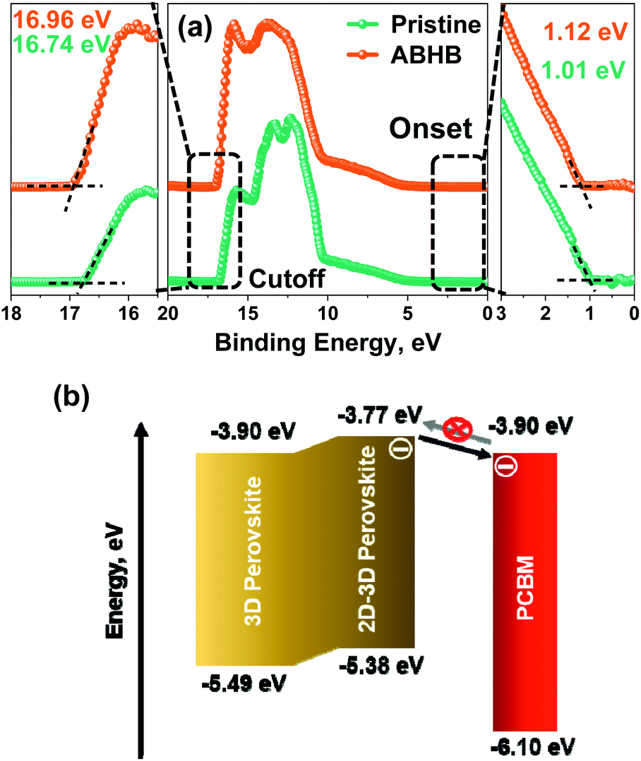 | ||
| Fig. 4 (a) UPS analysis of pristine and ABHB treated films. The cutoff (left) and onset (right) regions of UPS, and (b) schematic illustration of energy level alignment at the perovskite and PCBM interface. | ||
For more insight about the interfacial charge carrier dynamics, charge transport and defect passivation, the pristine and ABHB treated devices were characterized with a few specific analyses. Carrier extraction at the device interface was studied with Mott–Schottky (MS) analysis (Fig. 5a), from which the built-in potential (Vbi) and interfacial charge density (N) can be calculated using eqn (S2) (ESI†).42 ABHB treated devices reveal a higher Vbi value of 1.06 V than the pristine device (0.93 V) which leads to better VOC. The improved Vbi of the ABHB modified device is due to the thin 2D–3D graded perovskite heterostructure which leads to better charge separation, transportation, and collection. The pristine device reveals an N value of 6.81 × 1016 cm−3 which decreases to 3.17 × 1016 cm−3 after ABHB treatment. A reduced N indicates lower accumulation of charges at the interface because of effective charge extraction. This further confirms that more number of photogenerated charges are getting transported from the perovskite active layer.43 The capacitance–frequency (C–f) analysis shows that the ABHB treated device exhibits a lower capacitance in the low frequency region which further signifies better interfacial charge transport due to passivation of traps (Fig. 5b).44 This leads to improved JSC and reduced hysteresis of the ABHB treated device. Moreover, dark J–V measurements were performed to have better understanding about the charge transport behavior (Fig. 5c). The ABHB treated device exhibits a lower leakage current along with a decreased reverse saturation current resulting in lower charge recombination and enhanced carrier transport.
 | ||
| Fig. 5 (a) Mott–Schottky plots, (b) variation of C with frequency, (c) dark J–V characteristics of the devices with and without ABHB treatment, (d) Jphversus Veff characteristics with a double-logarithmic axis for the pristine and passivated device, (e) JSCversus light intensity plot, and (f) VOCversus light intensity plot. | ||
Fig. 5d shows the photocurrent density (Jph) versus effective voltage (Veff) plot, where Jph is the current density variation between dark and light and Veff is the variation between the applied voltage and the voltage at which Jph = 0. In the lower and higher (saturation region) Veff region, Jph is higher for the ABHB treated device which signifies an enhanced generation rate and results in improved JSC. Fig. 5e represents JSC measurements with respect to light intensity where the slope is near to unity for the ABHB treated device indicating better carrier transport due to lower recombinational loss. Fig. 5f reveals the VOCversus light intensity plot and can provide important understanding about the charge recombination mechanism.45 The obtained slopes for the pristine and ABHB treated devices were 1.57KBT/q and 1.24KBT/q, respectively (where KB, T, and q are the Boltzmann constant, absolute temperature and elementary charge respectively). The ABHB treated device exhibits an ideality factor closer to one whereas the pristine device reveals a higher value. From this result it can be said that recombination is largely suppressed for the ABHB treated device.
Impedance spectroscopy (IS) was performed to study about the charge recombination. Nyquist plots at various biases were taken for pristine and ABHB treated devices. All the curves were fitted with a corresponding circuit presented in the inset of Fig. 6a to acquire the values of recombination resistance (Rrec) and capacitance (C). The curve obtained at 0.75 V (Fig. 6a) reveals that there is a significant increase in Rrec in the ABHB treated device which indicates that the loss of the photogenerated charges has reduced leading to an increase in VOC. This is most likely due to the increase of the energy barrier at the 2D–3D graded perovskite. The changes of Rrec with applied bias, as revealed in Fig. 6b, show that the ABHB treated device exhibits a higher Rrec than the pristine device for all voltages. This signifies ABHB treatment can effectively suppress the charge recombination due to reduced defect states and better charge transfer ability. Fig. 6c illustrates the C versus applied bias plot where the pristine device shows a higher capacitance than the modified device. Hence, the probability of charge trapping is lower for the ABHB treated device. Further, trap density states (t-DOS) have been derived from the C versus applied bias plot (Fig. 6d) by exponential fitting of eqn (S3) (ESI†).38,46,47 In contrast to the pristine device, the modified device has lower t-DOS with narrower distribution which can be well correlated with the results attained from the Eu calculation. Besides, the narrower distribution confirms that the deep trap states in the ABHB modified device have reduced. Furthermore, the dark J–V measurements of the hole-only device (Fig. 6e and f) were used to extract the value of trap density (Nt) using eqn (S4) (ESI†). The pristine device exhibits a higher Nt of 7.99 × 1015 cm−3 than the ABHB treated device (3.14 × 1015 cm−3). Consequently, it is evident that the ABHB treated 2D–3D layer can significantly decrease the trap states in the perovskite and enhance the PSC device performance.
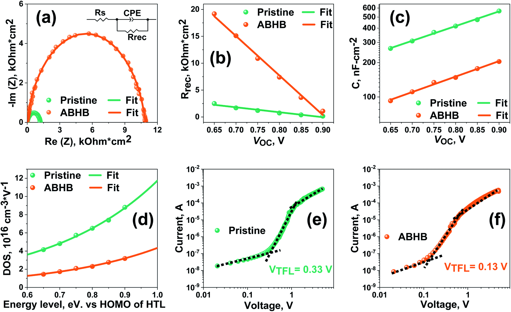 | ||
| Fig. 6 (a) Nyquist plots of the devices with and without ABHB. (b) Rrec variation with different biases, (c) variation of C with variable bias, and (d) trap density of states (DOS) versus electron energy level. (e and f) dark J–V characteristics from hole-only devices of pristine and ABHB modified devices respectively. | ||
Along with trap passivation and efficiency improvement, the upper 2D layer can efficiently restrict the moisture penetration into the lattice of the perovskite. To verify this, contact angle measurement has been carried out where the ABHB treated film reveals improved hydrophobicity with a higher contact angle of 87.5° than the pristine one with a contact angle of 46.1° (Fig. 7a). The stability of the films was further analyzed with XRD measurements where the films were stored at 40–50% relative humidity for a thousand hours (Fig. 7b). After aging, the XRD pattern of the ABHB treated film remains unchanged, whereas a strong peak for the PbI2 phase (degraded phase) appears for the pristine film. To validate these results, device stability was measured in a similar environment (Fig. 7c and S8, ESI†). For the ABHB treated device, all the device parameters (JSC, VOC and FF) exhibit almost negligible changes. Although, VOC remains nearly constant for the pristine device, all other device parameters start to degrade rapidly over time. Consequently, the ABHB treated device retains ∼95% of its initial efficiency; in contrast, the pristine device retains only ∼30%. This incredible enhancement of ambient stability upon ABHB treatment is due to the formation of the 2D layer over the 3D perovskite. A comparative table with recent literature of MAPbI3 based 2D–3D graded perovskites is presented in Table S2 (ESI†).
 | ||
| Fig. 7 (a) Contact angle measurement of pristine and ABHB treated films, (b) XRD patterns of perovskite films aged at a relative humidity of 40–50%, and (c) normalized VOC, JSC, FF and efficiency of pristine and ABHB modified devices aged at room temperature at a relative humidity of 40–50%. | ||
Conclusions
In summary, a facile and highly effective dimensionality engineering strategy has been established through which a 2D–3D graded heterostructure has been formed with improved surface morphology after precise treatment with ABHB. The amine and carboxylic acid groups effectively decrease the trap states while the bromide ions fill the halide vacancies by incorporating into the perovskite lattice. This 2D–3D perovskite efficiently minimizes carrier recombination, and offers enhanced charge transport and a higher generation rate. Consequently, the ABHB treated devices show outstanding efficiencies up to 21.18% (0.12 cm2) and 18.81% (2 cm2). Further, the devices with the 2D layer on top showed improved stability under ambient conditions due to better hydrophobicity. This method thus provides deeper insights into the dimensionality engineering strategy to develop 2D–3D graded perovskites for achieving high performance and stable photovoltaic devices, and it also has the potential to address the challenge of economical scalability.Conflicts of interest
There are no conflicts to declare.Acknowledgements
The authors acknowledge financial grants from DST, India through the projects DST/TSG/PT/2009/23, DST/CRG/2019/002164, Deity, India No. 5(9)/2012-NANO (Vol. II), Max- Planck-Gesellschaft IGSTC/MPG/PG(PKI)/2011A/48 and MHRD, India through SPARC project SPARC/2018-2019/P1097/SL. The Department of Chemistry, Centre for Nanotechnology and CIF, IIT Guwahati are acknowledged for instrument facilities.Notes and references
- B. Saparov and D. B. Mitzi, Chem. Rev., 2016, 116, 4558–4596 CrossRef CAS PubMed.
- Z. Xiao, C. Bi, Y. Shao, Q. Dong, Q. Wang, Y. Yuan, C. Wang, Y. Gao and J. Huang, Energy Environ. Sci., 2014, 7, 2619–2623 RSC.
- G. Xing, N. Mathews, S. Sun, S. S. Lim, Y. M. Lam, M. Grätzel, S. Mhaisalkar and T. C. Sum, Science, 2013, 342, 344 CrossRef CAS PubMed.
- W. Nie, H. Tsai, R. Asadpour, J.-C. Blancon, A. J. Neukirch, G. Gupta, J. J. Crochet, M. Chhowalla, S. Tretiak, M. A. Alam, H.-L. Wang and A. D. Mohite, Science, 2015, 347, 522 CrossRef CAS PubMed.
- A. Kojima, K. Teshima, Y. Shirai and T. Miyasaka, J. Am. Chem. Soc., 2009, 131, 6050–6051 CrossRef CAS PubMed.
- National Renewable Energy Laboratory, Best Research-Cell Efficiencies Chart, https://www.nrel.gov/pv/assets/pdfs/best-research-cell-efficiencies.20200104.pdf, accessed 24.04.2021 Search PubMed.
- E. H. Jung, N. J. Jeon, E. Y. Park, C. S. Moon, T. J. Shin, T.-Y. Yang, J. H. Noh and J. Seo, Nature, 2019, 567, 511–515 CrossRef CAS PubMed.
- N. J. Jeon, J. H. Noh, W. S. Yang, Y. C. Kim, S. Ryu, J. Seo and S. I. Seok, Nature, 2015, 517, 476–480 CrossRef CAS PubMed.
- Q. Jiang, Y. Zhao, X. Zhang, X. Yang, Y. Chen, Z. Chu, Q. Ye, X. Li, Z. Yin and J. You, Nat. Photonics, 2019, 13, 460–466 CrossRef CAS.
- B. Wang, M. Zhang, X. Cui, Z. Wang, M. Rager, Y. Yang, Z. Zou, Z. L. Wang and Z. Lin, Angew. Chem., Int. Ed., 2020, 59, 1611–1618 CrossRef CAS PubMed.
- X. Feng, R. Chen, Z.-A. Nan, X. Lv, R. Meng, J. Cao and Y. Tang, Adv. Sci., 2019, 6, 1802040 CrossRef PubMed.
- G. Grancini, C. Roldán-Carmona, I. Zimmermann, E. Mosconi, X. Lee, D. Martineau, S. Narbey, F. Oswald, F. De Angelis, M. Graetzel and M. K. Nazeeruddin, Nat. Commun., 2017, 8, 15684 CrossRef CAS PubMed.
- F. Tan, H. Tan, M. I. Saidaminov, M. Wei, M. Liu, A. Mei, P. Li, B. Zhang, C.-S. Tan, X. Gong, Y. Zhao, A. R. Kirmani, Z. Huang, J. Z. Fan, R. Quintero-Bermudez, J. Kim, Y. Zhao, O. Voznyy, Y. Gao, F. Zhang, L. J. Richter, Z.-H. Lu, W. Zhang and E. H. Sargent, Adv. Mater., 2019, 31, 1807435 CrossRef PubMed.
- M. Abdi-Jalebi, M. Ibrahim Dar, S. P. Senanayak, A. Sadhanala, Z. Andaji-Garmaroudi, L. M. Pazos-Outón, J. M. Richter, A. J. Pearson, H. Sirringhaus, M. Grätzel and R. H. Friend, Sci. Adv., 2019, 5, eaav2012 CrossRef CAS PubMed.
- P. Guo, Q. Ye, X. Yang, J. Zhang, F. Xu, D. Shchukin, B. Wei and H. Wang, J. Mater. Chem. A, 2019, 7, 2497–2506 RSC.
- X. Wu, L. Zhang, Z. Xu, S. Olthof, X. Ren, Y. Liu, D. Yang, F. Gao and S. Liu, J. Mater. Chem. A, 2020, 8, 8313–8322 RSC.
- M. Hossain, R. Garai, R. K. Gupta, R. Narasimhan and P. K. Iyer, J. Mater. Chem. C, 2021, 9, 10406–10413 RSC.
- B. Wang, H. Li, Q. Dai, M. Zhang, Z. Zou, J.-L. Brédas and Z. Lin, Angew. Chem., Int. Ed., 2021, 60, 17664–17670 CrossRef CAS PubMed.
- X. Wen, J. Wu, M. Ye, D. Gao and C. Lin, Chem. Commun., 2016, 52, 11355–11358 RSC.
- L.-B. Huang, P.-Y. Su, J.-M. Liu, J.-F. Huang, Y.-F. Chen, S. Qin, J. Guo, Y.-W. Xu and C.-Y. Su, J. Power Sources, 2018, 378, 483–490 CrossRef CAS.
- M. Li, X. Yan, Z. Kang, Y. Huan, Y. Li, R. Zhang and Y. Zhang, ACS Appl. Mater. Interfaces, 2018, 10, 18787–18795 CrossRef CAS PubMed.
- M. Kim, S. G. Motti, R. Sorrentino and A. Petrozza, Energy Environ. Sci., 2018, 11, 2609–2619 RSC.
- Y. Lv, Y. Shi, X. Song, J. Liu, M. Wang, S. Wang, Y. Feng, S. Jin and C. Hao, ACS Appl. Mater. Interfaces, 2018, 10, 31755–31764 CrossRef CAS PubMed.
- Q. He, M. Worku, L. Xu, C. Zhou, H. Lin, A. J. Robb, K. Hanson, Y. Xin and B. Ma, ACS Appl. Mater. Interfaces, 2020, 12, 1159–1168 CrossRef CAS PubMed.
- M. Kim, G.-H. Kim, T. K. Lee, I. W. Choi, H. W. Choi, Y. Jo, Y. J. Yoon, J. W. Kim, J. Lee, D. Huh, H. Lee, S. K. Kwak, J. Y. Kim and D. S. Kim, Joule, 2019, 3, 2179–2192 CrossRef CAS.
- D. Lin, T. Zhang, J. Wang, M. Long, F. Xie, J. Chen, B. Wu, T. Shi, K. Yan, W. Xie, P. Liu and J. Xu, Nano Energy, 2019, 59, 619–625 CrossRef CAS.
- Y. Cho, A. M. Soufiani, J. S. Yun, J. Kim, D. S. Lee, J. Seidel, X. Deng, M. A. Green, S. Huang and A. W. Y. Ho-Baillie, Adv. Energy Mater., 2018, 8, 1703392 CrossRef.
- P. Chen, Y. Bai, S. Wang, M. Lyu, J.-H. Yun and L. Wang, Adv. Funct. Mater., 2018, 28, 1706923 CrossRef.
- F. S. Ghoreishi, V. Ahmadi, R. Poursalehi, M. SamadPour, M. B. Johansson, G. Boschloo and E. M. J. Johansson, J. Power Sources, 2020, 473, 228492 CrossRef CAS.
- H.-C. Chen, J.-M. Lan, H.-L. Hsu, C.-W. Li, T.-S. Shieh, K.-T. Wong and C.-P. Chen, Mater. Chem. Front., 2021, 5, 3378–3387 RSC.
- N. Wei, Y. Chen, Y. Miao, T. Zhang, X. Wang, H. Wei and Y. Zhao, J. Phys. Chem. Lett., 2020, 11, 8170–8176 CrossRef CAS PubMed.
- X. Jiang, S. Chen, Y. Li, L. Zhang, N. Shen, G. Zhang, J. Du, N. Fu and B. Xu, ACS Appl. Mater. Interfaces, 2021, 13, 2558–2565 CrossRef CAS PubMed.
- M. A. Afroz, R. Garai, R. K. Gupta and P. K. Iyer, ACS Appl. Energy Mater., 2021, 4, 10468–10476 CrossRef CAS.
- L. Zhang, K. Cao, J. Qian, Y. Huang, X. Wang, M. Ge, W. Shen, F. Huang, M. Wang, W. Zhang, S. Chen and T. Qin, J. Mater. Chem. C, 2020, 8, 17482–17490 RSC.
- L. Lin, J. T.-W. Wang, T. W. Jones, M. Grigore, A. Cook, D. W. deQuilettes, R. Brenes, B. C. Duck, K. F. Anderson, N. W. Duffy, B. Wenger, V. Bulović, J. Pu, J. Li, B. Chi, H. J. Snaith and G. J. Wilson, J. Mater. Chem. A, 2019, 7, 25511–25520 RSC.
- R. K. Gupta, R. Garai, M. Hossain, A. Choudhury and P. K. Iyer, ACS Sustainable Chem. Eng., 2021, 9, 7993–8001 CrossRef CAS.
- R. Garai, R. K. Gupta, A. S. Tanwar, M. Hossain and P. K. Iyer, Chem. Mater., 2021, 33, 5709–5717 CrossRef CAS.
- R. Garai, M. A. Afroz, R. K. Gupta and P. K. Iyer, Adv. Sustainable Syst., 2020, 4, 2000078 CrossRef CAS.
- M. A. Afroz, R. K. Gupta, R. Garai, M. Hossain, S. P. Tripathi and P. K. Iyer, Org. Electron., 2019, 74, 172–178 CrossRef CAS.
- M. Hossain, R. N. Arunagirinathan, R. Garai, R. K. Gupta and P. K. Iyer, J. Mater. Chem. C, 2021, 9, 14309–14317 RSC.
- J.-W. Lee, Z. Dai, T.-H. Han, C. Choi, S.-Y. Chang, S.-J. Lee, N. De Marco, H. Zhao, P. Sun, Y. Huang and Y. Yang, Nat. Commun., 2018, 9, 3021 CrossRef PubMed.
- R. K. Gupta, R. Garai and P. K. Iyer, ACS Appl. Energy Mater., 2021, 4, 10025–10032 CrossRef CAS.
- J. Xie, P. Hang, H. Wang, S. Zhao, G. Li, Y. Fang, F. Liu, X. Guo, H. Zhu, X. Lu, X. Yu, C. C. S. Chan, K. S. Wong, D. Yang, J. Xu and K. Yan, Adv. Mater., 2019, 31, 1902543 CrossRef PubMed.
- O. Almora, C. Aranda, E. Mas-Marzá and G. Garcia-Belmonte, Appl. Phys. Lett., 2016, 109, 173903 CrossRef.
- R. K. Gupta, R. Garai, M. A. Afroz and P. K. Iyer, J. Mater. Chem. C, 2020, 8, 8191–8198 RSC.
- A. Choudhury, R. K. Gupta, R. Garai and P. K. Iyer, Adv. Mater. Interfaces, 2021, 8, 2100574 CrossRef CAS.
- B. C. O'Regan, S. Scully, A. C. Mayer, E. Palomares and J. Durrant, J. Phys. Chem. B, 2005, 109, 4616–4623 CrossRef PubMed.
Footnote |
| † Electronic supplementary information (ESI) available: Experimental details, XRD peak intensity, FTIR, device architecture, device parameters, box chart, large area J–V, device parameters under ambient conditions, and literature comparison tables. See DOI: 10.1039/d1ta06901b |
| This journal is © The Royal Society of Chemistry 2021 |