
Merged interface construction toward ultra-low Voc loss in inverted two-dimensional Dion–Jacobson perovskite solar cells with efficiency over 18%†
Haotian
Wu
abc,
Xiaomei
Lian
abc,
Jun
Li
abc,
Yingzhu
Zhang
abc,
Guanqing
Zhou
abc,
Xinbo
Wen
abc,
Zengqi
Xie
 abc,
Haiming
Zhu
*abc,
Gang
Wu
*abc and
Hongzheng
Chen
*abc
abc,
Haiming
Zhu
*abc,
Gang
Wu
*abc and
Hongzheng
Chen
*abc
aState Key Laboratory of Silicon Materials, MOE Key Laboratory of Macromolecular Synthesis and Functionalization, Department of Polymer Science and Engineering, Zhejiang University, Hangzhou 310027, P. R. China. E-mail: wmang@zju.edu.cn; hzchen@zju.edu.cn
bDepartment of Chemistry, Zhejiang University, Hangzhou 310027, P. R. China. E-mail: hmzhu@zju.edu.cn
cInstitute of Polymer Optoelectronic Materials and Devices & State, Key Laboratory of Luminescent Materials and Devices, South China University of Technology, Guangzhou 510640, P. R. China
First published on 11th May 2021
Abstract
An optimized interface between a perovskite and a charge transport layer with full contact and low defect density favors an improvement in performance of perovskite solar cells (PVSCs). However, few works have been reported on constructing an interface for efficient charge transport and low energy loss in 2D Dion–Jacobson (DJ) PVSCs with an inverted structure. Herein, a deposition process combining pre-annealing and merged annealing (PMA) was demonstrated to be effective in constructing a merged interface between the layers of an electron transport material, PC61BM, and DJ perovskite (3AMP)(MA0.75FA0.25)3Pb4I13, which promotes perovskite/PC61BM contact and thus improves defect passivation and charge transport. A high Voc (1.24 V) with ultra-low energy loss (0.35 eV) is achieved because of the decreased defect density. A PMA-based device with a structure of ITO/(NiOx/PTAA)/perovskite/PC61BM/BCP/Ag exhibits a highest PCE of 18.67%, which is the highest value among the 2D DJ PVSCs with an inverted structure. The device retains 90% of its initial PCE after storage in air with a humidity of 45 ± 5% for 60 days or in an 85 °C N2 atmosphere for 480 h, and remains unchanged in 50 cycles of thermal cycling measurements. This work provides an effective approach towards 2D DJ PVSCs with both high efficiency and high moisture and thermal stability.
Introduction
An organic–inorganic hybrid perovskite has been successfully applied in solar cells due to its high absorption coefficient, high carrier migration rate and high fault tolerance, and is considered to be one of the most promising materials for next-generation photovoltaic technology.1–4 With the rapid improvement in the power conversion efficiency (PCE) of perovskite solar cells (PVSCs), more attention has been paid to the stability of the devices.Two-dimensional (2D) perovskites exhibit excellent environmental stability because of the high formation energy and strong hydrophobicity introduced by organic spacer cations.5–13 However, the insulating spacer cation layer blocks the transport of photogenerated carriers and hinders any improvement in the PCEs of 2D PVSCs.14–16 2D Dion–Jacobson (DJ) perovskites with the chemical formula ABn−1MnX3n+1, applying diammonium as an A-site spacer cation, have a relatively shorter distance between the adjacent [Bn−1MnX3n+1]2− slabs compared to their counterparts with a Ruddlesden–Popper structure. The decreased interlayer distance, together with the resulting weakened quantum confinement effect and the narrowed bandgap, will benefit charge separation/transport and light harvesting as well, which shows potential in PCE elevation.17,18 The efforts for elevating the PCE of 2D DJ PVSCs are now mostly focused on improving the charge-transportation inside the perovskite film to increase the short-circuit current density (Jsc) by fabricating high-quality film with a vertical growth orientation.19–22 The developed methods include hot-casting,5,19,23 additives and anti-solvent assistance,24–26 solvent vapor annealing,27 and selecting suitable spacer cations.28,29 In addition, Li et al. reported the first example of formamidinium (FA) based 2D DJ PVSC with excellent moisture stability, the photovoltaic performance of which depends on the unique phase structure of the light-harvesting material.30,31
A high open-circuit voltage (Voc) is indispensable for the efficiency improvement of 2D PVSCs, considering the relatively wide bandgap of 2D perovskites. However, the Voc of most 2D DJ PVSCs are around 1.0 V to 1.1 V (see Table S1†), even lower than for some MAPbI3-based devices.32,33 This indicates that 2D PVSCs suffer severe Voc losses, at least, compared to 3D PVSCs with high performance. Even for the best 2D DJ PVSCs, the value of Voc loss is up to 0.4–0.5 eV,26–29 as listed in Table S1.† A relatively low Voc value is currently the bottleneck for further improvement in the PCE. The Voc losses can be ascribed to non-radiative recombination via defect states at the grain boundaries of the perovskite film and at their interfaces with the charge transport layer. Most recently, He et al. achieved a homogeneous energy landscape and decreased defect density by regulating the crystallization kinetics of a meta-(aminomethyl)piperidinium-based 2D DJ perovskite. A high Voc of 1.21 V induced by reduced nonradiative recombination was reported.29
From the viewpoint of interface engineering, insertion of an ultrathin passivation layer between the perovskite and charge transport material was proved to be effective in elevating Voc,34–36 but hindered charge extraction.33 [6,6]-Phenyl-C61-butyric acid methyl ester (PC61BM), as an effective electron transport material, was demonstrated to be a Lewis acid passivator that can reduce halide-induced traps.37,38 But, for a PC61BM layer spin-coated on a perovskite film with a smooth surface the passivation effect is restricted by the limited contact area of the interface. Enlarging the perovskite/PC61BM interface will favor both charge transport and defect passivation, but faces difficulties in 2D DJ perovskites. Due to the lack of van der Waals forces, it is more difficult for 2D DJ perovskites to form an ordered structure with high crystallinity and good orientation, compared to their counterparts with an RP structure. The variation in the interface layer might introduce more uncontrollable factors into the crystallization process, harmful to the formation of a high-quality film. Up to now, there has still been no report about interface engineering for 2D DJ PVSCs, although the interface layer is regarded as one of the key factors that influences the charge extraction and determines the surface trap density and the resulting energy loss.39–41
In this work, a merged interface between PC61BM and a (3AMP)(MA0.75FA0.25)3Pb4I13 perovskite was constructed via a new two-step merged annealing method on the basis of ensuring the high quality of the 2D DJ perovskite film. Because of the optimized interface with decreased defect density, a high Voc (1.24 V) and low energy loss (0.35 eV) were achieved, both of which are the best results for 2D DJ PVSCs. A device with a structure of ITO/(NiOx/PTAA)/perovskite/PC61BM/BCP/Ag exhibited a PCE of 18.67%, which is the highest value among 2D DJ PVSCs with an inverted structure.
Results and discussion
Fig. 1 presents three different fabrication processes for (3AMP)(MA0.75FA0.25)3Pb4I13 film coated with an electron transport layer (ETL), i.e. PC61BM in this study. Route I is the conventional annealing method (abbreviated as CA), in which PC61BM is deposited onto the fully annealed perovskite film. Route II is the merged annealing method (abbreviated as MA), in which solutions of precursor and PC61BM are spin-coated in sequence and then annealed together.42,43 Route III is a combination of pre-annealing and merged annealing, in which the spin-coated precursor solution is pre-annealed for a very short time, followed by spin-coating of PC61BM, and then PC61BM and the pre-annealed precursor experience the merged annealing process together. Route III is abbreviated as PMA for convenience. A high-quality perovskite film with a merged interface between ETL and perovskite is expected to be constructed through an MA or PMA process.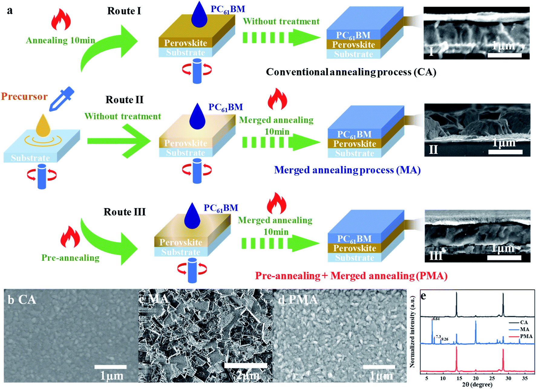 | ||
| Fig. 1 (a) Schematic illustration of three fabrication processes for a PC61BM coated (3AMP)(MA0.75FA0.25)3Pb4I13 film and the cross-sectional SEM images for the corresponding films. Top-view SEM images of (3AMP)(MA0.75FA0.25)3Pb4I13 films fabricated by CA (b), MA (c) and PMA (d) processes. (e) X-ray diffraction (XRD) patterns of perovskite films fabricated by various methods. | ||
The cross-sectional SEM images of (3AMP)(MA0.75FA0.25)3Pb4I13 films prepared by various methods are shown in Fig. 1a. It is found that both CA and PMA processes help to form perovskite film with a compact structure (Fig. 1a(I) and (III)). But the MA-based film presents an extremely poor morphology. The film cannot completely cover the substrate, as shown in Fig. 1a(II). Large amounts of gaps and holes can be observed in the film surface (Fig. 1c). As a result, the substrate can be seen in the enlarged image shown in Fig. S1a† The corresponding X-ray diffraction (XRD) patterns are presented in Fig. 1e For the MA-based film: besides the 14.08° and 28.32° peaks for the (011) and (022) lattice planes of (3AMP)(MA0.75FA0.25)3Pb4I13 perovskite,18 the diffraction peaks at 2θ of 6.64°, 7.3° and 9.26° can be attributed to the residue of the intermediates of MAI–PbI2–DMSO,44,45 which can be observed in the enlarged SEM image (Fig. S1b†). It is suggested that the MA process hindered the transition of the intermediate to final perovskite. For the films prepared by CA and PMA methods, no intermediate residue can be detected. The diffraction peaks of the (011) and (022) lattice plane in the PMA-based film are obviously strengthened, compared to the MA-based film, indicating the preferred orientation of the crystal structure for the (3AMP)(MA0.75FA0.25)3Pb4I13 film via the PMA process.24,46 In addition, the steady-state photoluminescence spectra (PL) of the PMA-based film shows no peaks for the quantum wells of low n values no matter whether back (glass side) or front (perovskite side) excitation was used (Fig. S2†). This implies that the film structure should be relatively uniform from the top to the bottom of the entire perovskite film, as reported in previous studies.24,26 The top-view images of the CA- and PMA-based perovskite films, where the top PC61BM was rinsed away, are shown in Fig. 1b and d. The variation in grain size is not obvious. The surface of the PMA-based film is rougher than that of the CA-based film. The root mean square surface roughness values of the PMA- and CA-based films are 14.2 nm and 11.1 nm, according to the corresponding AFM images shown in Fig. S3,† which could be attributed to the penetration of PC61BM inside the surface layer of (3AMP)(MA0.75FA0.25)3Pb4I13 and the formation of the merged interface between perovskite and PC61BM.
Then, we fabricated a device with the inverted structure of ITO/(NiOx/PTAA)/perovskite/PC61BM/BCP/Ag, as shown in Fig. 2a, using (3AMP)(MA0.75FA0.25)3Pb4I13 as the absorber layer, the UV-vis absorption spectra of which are shown in Fig. S4.† The perovskite/PC61BM layer was deposited separately by CA and PMA processes. The current density–voltage (J–V) curves of the corresponding devices are shown in Fig. 2b. The detailed photovoltaic parameters are summarized in Table 1. The best power conversion efficiency (PCE) of the CA-based devices is 16.92%, with an open-circuit voltage (Voc) of 1.20 V, short-circuit current density (Jsc) of 18.6 mA cm−2 and fill factor (FF) of 75.86%. The PMA-based device exhibits an increased Jsc of 19.51 mA cm−2 and Voc of 1.24 V. The distribution diagrams of Voc, Jsc and FF are shown in Fig. S5a–c.† A champion PCE of 18.67% with an average value of 18.25% were achieved. Both PCE and Voc are the best values for 2D DJ PVSCs. The device's PCE was certified to be 17.86% (Fig. S6†). The stable photocurrent and steady efficiency at the maximum power point of 0.99 V were obtained during 300 s, resulting in a stabilized PCE of 17.62%, as shown in Fig. S5d.† Furthermore, the PMA-based device exhibits a larger shunt resistance (Rsh) and a smaller series resistance (Rs), as listed in Table 1, indicating better film morphology and more efficient charge extraction/transport than the CA-based one. Fig. S7† shows the forward and reverse scanning J–V curves of the devices fabricated using CA and PMA methods. The PMA-based device presents a hysteresis index of 4.2%, lower than that of the CA-based device (9.1%). Fig. 2c shows the external quantum efficiency (EQE) spectra and the corresponding integrated photocurrent curves. The EQE curves exhibit the same cut-off edge as the absorption spectra (Fig. S4†). The integrated photocurrents for PMA- and CA-based devices are 19.38 mA cm−2 and 18.43 mA cm−2, respectively, both of which closely match the Jsc values from J–V curves. The PCE histogram of the 30 devices prepared from different processes in Fig. 2d indicates that PMA-based devices exhibit a narrower distribution, indicating better reproducibility.
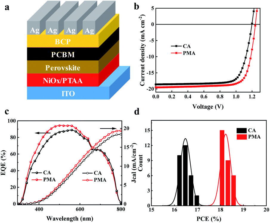 | ||
| Fig. 2 Planar structured PVSC device configuration (a), J–V curves (b), EQE spectra and the integrated photocurrent curves (c) of the CA and PMA based devices, and PCE histogram of 30 devices fabricated by the CA or PMA process (d). | ||
| V oc (V) | J sc (mA cm−2) | FF (%) | PCE (%) | R s (Ω) | R sh (Ω) | ||
|---|---|---|---|---|---|---|---|
| CA | Max | 1.20 | 18.61 | 75.86 | 16.92 | 146.63 | 38![[thin space (1/6-em)]](https://www.rsc.org/images/entities/char_2009.gif) 756.42 756.42 |
| Average | 1.18 | 19.20 | 73.06 | 16.47 | — | — | |
| PMA | Max | 1.24 | 19.51 | 77.27 | 18.67 | 106.65 | 68349.61 |
| Average | 1.23 | 19.91 | 74.27 | 18.25 | — | — | |
Ultrafast transient absorption spectroscopy (TAS) has been carried out to study the effect of the deposition process on the internal charge transfer dynamics in perovskite films. TA spectra and kinetics of devices fabricated by CA and PMA approaches are shown in the upper and lower panels of Fig. 3, respectively. From TAS results (Fig. 3a, b, d and e), after photoexcitation with 365 nm light, the TA spectra of these films show ground-state bleaching (GSB) peaks at 605 nm, 625 nm, 655 nm and 740 nm, which could be assigned to different 2D perovskites with n = 2, n = 3, n = 4, and n = ∞, respectively. The rising and decay kinetics of perovskite components of different n are shown in Fig. 3c–f. From the TA kinetics, the fast decay of the TA signal from smaller n species is accompanied by a fast rise in larger n species, indicating the charge transfer process from smaller n to larger n species. The transfer time between different n species can be obtained by exponential fitting on TA kinetics and the results are listed in Table S2.† Interestingly, charge transfer between different n species is much faster in PMA-perovskites than in a CA-device, regardless of n value. The same trend can be seen for different n values. For example, the transfer time to n = ∞ is shortened from 21 ps in PMA- to 13 ps in CA-based devices. The improved internal charge transfer in PMA film indicates improved physical contact and electronic interaction between different n species in PMA-perovskites.46–48 To further inspect the influence of the fabrication process on the interfacial carrier extraction by the PC61BM layer, steady-state and time-resolved PL were measured. Significant PL quenching (Fig. S8a†) and much faster PL decay (Fig. S8b and Table S3†) can be observed for PMA-film, indicating improved charge transfer from perovskite to PC61BM. The results of TAS and PL are consistent with the promotion of Jsc for the PMA-based device.
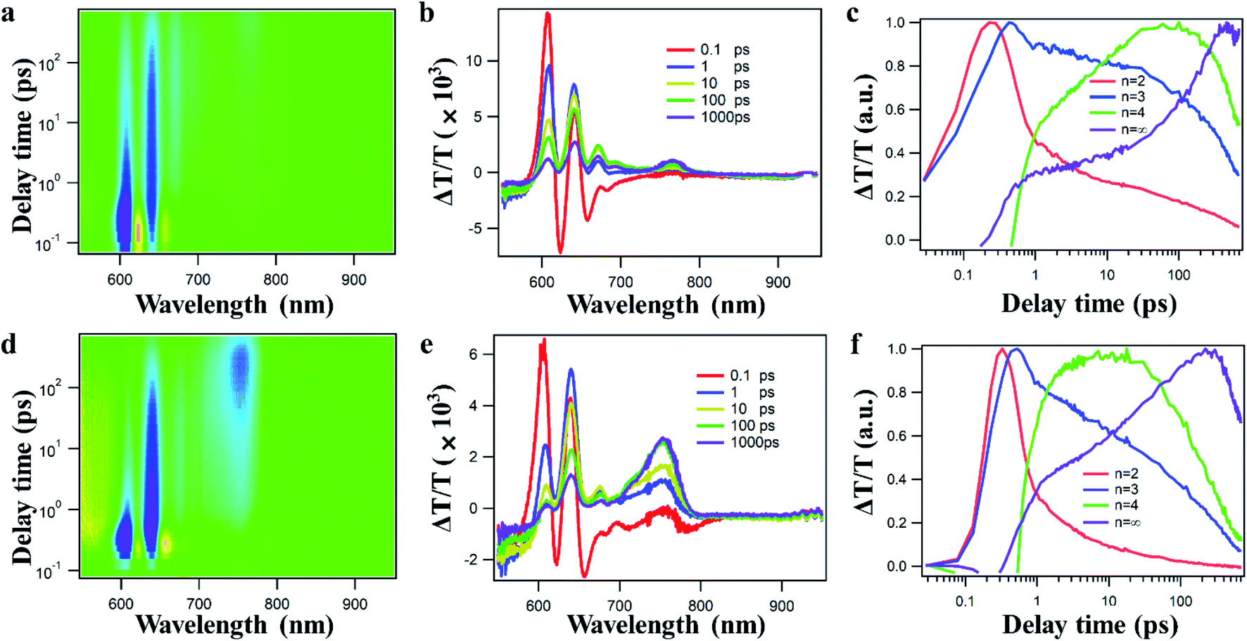 | ||
| Fig. 3 2D color plot of TA spectra (left), representative TA spectra at indicated delay times (middle), and TA kinetics probed at different-n perovskite bands (right) obtained by irradiating the perovskite films using a 365 nm laser with a fluence below 1 μJ cm−2 from the back (glass). (a–c) Device fabricated by CA, (d–f) device fabricated by PMA. | ||
The PL spectra of the CA- and PMA-based films are shown in Fig. S9.† The samples were rinsed with chlorobenzene to remove unbounded PC61BM. The PL intensity of the PMA-based film is much lower than that of the CA-based film, due to the charge transfer from perovskite to PC61BM. The residue of PC61BM penetrating into the perovskite film could suggest the formation of a merged interface. TOF-SIMS measurement of the CA- and PMA-based films coated with PC61BM was carried out to track the depth distributions of C8− and PbI− from the top of the PC61BM layer down to the perovskite (Fig. S10†). The PbI− and C8− signals were applied as tracers for perovskite and PC61BM, respectively. From the time point indicated by the black arrow, the intensity of the C8− signal decreases with increasing PbI− intensity. When the PbI− intensity reaches its maximum (shown by the red arrow), the reduction amplitude of the intensity of C8− signal (labeled as ΔC8−) for the PMA-based film is much smaller than that of the CA-based film, indicating the deeper penetration of PC61BM inside the perovskite layer induced by the PMA process.49 The corresponding X-ray photoelectron spectroscopy (XPS) is displayed in Fig. 4a and b. The peaks of I 3d and Pb 4f for PMA-based film are both shifted to higher binding energies compared to the CA counterpart, indicating enhanced interaction between the perovskite and PC61BM,50,51 which can be attributed to the formation of the merged interface, which improves the interface contact and enlarges the contact area between perovskite and PC61BM. It is reported that PC61BM plays a passivating role at iodide-rich trap sites on the surface of perovskite.38 The formation of a merged interface could promote the passivation effect of PC61BM on the defects at the interface and grain boundaries. Besides this, according to the PL emission peak, the bandgap of the film can be calculated to be 1.59 eV.52 It is worth noting that the Voc loss of the PMA-based device, 0.35 eV, is much lower than that of reported 2D DJ PVSCs, as listed in Table S1,† and is even the lowest value among 2D PVSCs. This result could be attributed to the formation of the merged interface and the resulting suppressed recombination as supported by the following discussion.
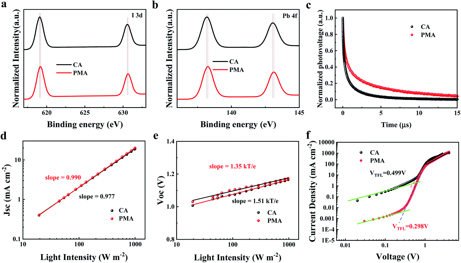 | ||
| Fig. 4 I 3d core level (a), Pb 4f core level (b) XPS spectra of the CA- and PMA-based perovskite films with the PC61BM layer rinsed away. (c) TPV decay curves of the devices fabricated by CA and PMA processes. Measured Jsc (d), Voc (e) of CA- and PMA-based devices plotted against light intensity (dots), together with linear fits (solid lines) to the data. (f) J–V curves of the electron-only devices fabricated by CA and PMA processes. | ||
Transient photovoltage (TPV) measurement was used to investigate the charge recombination kinetics inside the devices. As displayed in Fig. 4c, the PMA-based device displays a longer decay life of 1.99 ns, compared to 0.63 ns for the CA-based device, which reveals slower recombination kinetics and less energy loss,46,53 resulting from the passivation of the defects at the interface. This indicates that the PMA process and the resulting merged interface can suppress the charge recombination and reduce energy loss, which favors the elevation of Voc. The light intensity dependence of Jsc and Voc was measured to study the recombination kinetics in photovoltaic devices. The relationship between Jsc and light intensity (Fig. 4d) indicates that the slope values for the PMA- and CA-based devices were 0.990 and 0.977, respectively, demonstrating negligible bimolecular recombination during charge transport. As shown in Fig. 4e, the slope of Vocversus the logarithm of the light intensity for the PMA-based device is 1.35kT/q (k is Boltzmann constant, T is temperature, and q is an elementary charge), which is smaller than that of the CA-based device (1.51kT/q), indicating that the recombination caused by defects is suppressed, which contributes to the elevation of Voc.
Space charge limited current (SCLC) measurements were carried out on electron-only devices with a structure of ITO/SnO2/perovskite/PC61BM/BCP/Ag, based on the PMA and CA processes, and the results are shown in Fig. 4f. The trap state density (Nt) was determined according to the following equation, Nt = 2ε0εrVTFL/qL2, where ε0 is the vacuum permittivity, εr is the relative dielectric constant, VTFL is the onset voltage of the TFL region, q is the elemental charge and L is the thickness of the film. The CA- and PMA-based devices exhibit VTFL of 0.499 V and 0.298 V, with corresponding Nt of 9.18 × 1015 cm−3 and 5.49 × 1015 cm−3, respectively. The dark current level of the PMA-based device is lower than that of the CA-based device, as shown in Fig. S11,† indicating the suppressed charge recombination consistent with the low trap density of the PMA-based film. The PMA process induced decrease in trap state density can be ascribed to the defect passivation at the interface between perovskite and PC61BM resulting from the formation of a merged interface and the interaction between PC61BM and the perovskites.
Transient photocurrent (TPC) measurements were used to investigate the charge extraction process inside the devices. The TPC results (Fig. S12a†) show that the carrier transport time is 0.29 ns for the PMA-based device, shorter than for the CA-based device (0.53 ns), indicating more efficient charge extraction, agreeing well with the results of TAS. The relationship between charge collection probability (Pc) and internal voltage (Vint) under the condition of 100 mW cm−2 is presented in Fig. S12b.†54Pc can be calculated from Pc = Jph/Jphsat. JPh (photocurrent density) is defined as Jl − Jd, where Jd and Jl are the current of the device in dark and light states, respectively. Jphsat is the saturation current density under a negative bias voltage (−0.5 V). Vint is defined as Vint = Vbi − Vapp, in which Vbi is the built-in electric field potential (that is, the voltage when Jph is equal to 0), and Vapp is the applied voltage. As shown in Fig. S12b,† in the range from open circuit to short circuit, the Pc of the PMA-based device is higher than that of the CA-based device. When Vint is 0.09 and 0.21 V, the PMA-based device exhibits higher Pc value (45% and 82%), compared to the Pc value (35% and 68%) of the CA-based device, indicating that the PMA process successfully improves the efficiency of carrier collection,55,56 agreeing well with the TPC results and the increase in Jsc.
Finally, the effect of the PMA process on the stability of the perovskite film and the device under various conditions was explored. To evaluate the moisture resistance, the color of the CA- and PMA-based films (coated with PC61BM) was recorded when exposed to an air atmosphere with humidity of about 70%. As shown in Fig. S13,† a color change can be observed for the CA-based film after 15 min. But for the PMA-based film, the color remains almost unchanged within 50 min. The 2D PVSCs based on (3AMP)(MA0.75FA0.25)3Pb4I13 also exhibits superior stability, compared to the device based on 3D MA0.75FA0.25PbI3 perovskite (Fig. 5a and b). When exposed to air atmosphere with a humidity of 45 ± 5%, the CA-based device dropped to about 60% of the initial PCE after 60 days of storage. Under the same conditions, the unencapsulated PMA-based device exhibits better moisture stability so that 90% of the original efficiency was retained. The improved moisture resistance could be attributed to the formation of the merged interface which can act as a sealing layer to better prevent the perovskite layer coming into direct contact with the moist atmosphere. This improved sealing effect favors the elevation of thermal stability of the PMA-based perovskite film and the device as well. The color change of the PMA-based film at 200 °C is slower than that of the CA-based film (Fig. S14†). The unencapsulated PMA-based devices in the N2 box retains 90% of initial PCE after 480 h of treatment at 85 °C, while the CA-based device lost 20% of the original efficiency. Considering the temperature difference between day and night that the device will experience in practical application, the variation of the PCE under thermal cycles of different temperature ranges (−10–10 °C and 10–50 °C) was tested. The results in Fig. 5d show that the PMA-based device can withstand 50 times of thermal-cycling without PCE loss, indicating good stability in working day and night, suggesting its potential for use in future practical applications.
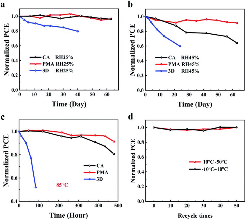 | ||
| Fig. 5 Stability measurements: (a) at room temperature with humidity 25 ± 5%, (b) at room temperature with humidity of 45 ± 5%, (c) at 85 °C in an N2-filled glovebox for the 3D and 2D PVSCs. (d) Thermal-cycling test for the PMA-based device. | ||
Conclusions
In conclusion, a merged interface between electron transport layer and high-quality (3AMP)(MA0.75FA0.25)3Pb4I13 perovskite film was constructed via the deposition process combining pre-annealing and merged annealing. The penetration of PC61BM inside the perovskite layer enlarged the contact area between the light harvesting layer and the ETL, which increases the channels for efficient charge transport and elevates the passivation effect of PC61BM on the defects at the grain boundary and interface. The PMA-based device with a structure of ITO/(NiOx/PTAA)/perovskite/PC61BM/BCP/Ag presents a high Voc (1.24 V) and an ultra-low energy loss (0.35 eV), both of which are the best results for 2D DJ PVSCs. A high PCE of 18.67% with a certified value of 17.86% reached the highest level for 2D DJ PVSCs with an inverted structure. The device exhibits an impressive stability so that 90% of initial PCE was retained after storage in air with a humidity of 45 ± 5% for 60 days or in 85 °C N2 atmosphere for 480 h. The efficiency of the device remains almost unchanged after 50 thermal cycle measurements.Conflicts of interest
There are no conflicts to declare.Acknowledgements
This work is supported by the National Natural Science Foundation of China (No. 51973184, 51961145301, 51620105006, 61721005), the National Key Research and Development Program of China (No. 2019YFA0705900) and the Key Research Project of Southern Xinjiang (Grant No. 2019DB013).Notes and references
- M. Jeong, I. W. Choi, E. M. Go, Y. Cho, M. Kim, B. Lee, S. Jeong, Y. Jo, H. W. Choi, J. Lee, J.-H. Bae, S. K. Kwak, D. S. Kim and C. Yang, Science, 2020, 369, 1615–1620 CrossRef CAS PubMed.
- G. Kim, H. Min, K. S. Lee, D. Y. Lee, S. M. Yoon and S. I. Seok, Science, 2020, 370, 108–112 CrossRef CAS PubMed.
- Z. Liu, L. Qiu, L. K. Ono, S. He, Z. Hu, M. Jiang, G. Tong, Z. Wu, Y. Jiang, D.-Y. Son, Y. Dang, S. Kazaoui and Y. Qi, Nat. Energy, 2020, 5, 596–604 CrossRef CAS.
- H. Fan, F. Li, P. Wang, Z. Gu, J.-H. Huang, K.-J. Jiang, B. Guan, L.-M. Yang, X. Zhou and Y. Song, Nat. Commun., 2020, 11, 5402 CrossRef CAS PubMed.
- H. Tsai, W. Nie, J.-C. Blancon, C. C. Stoumpos, R. Asadpour, B. Harutyunyan, A. J. Neukirch, R. Verduzco, J. J. Crochet, S. Tretiak, L. Pedesseau, J. Even, M. A. Alam, G. Gupta, J. Lou, P. M. Ajayan, M. J. Bedzyk, M. G. Kanatzidis and A. D. Mohite, Nature, 2016, 536, 312–316 CrossRef CAS PubMed.
- X. Zhang, G. Wu, S. Yang, W. Fu, Z. Zhang, C. Chen, W. Liu, J. Yan, W. Yang and H. Chen, Small, 2017, 13, 1700611 CrossRef PubMed.
- J. Shi, Y. Gao, X. Gao, Y. Zhang, J. Zhang, X. Jing and M. Shao, Adv. Mater., 2019, 31, 1901673 CrossRef PubMed.
- X. Zhang, G. Wu, W. Fu, M. Qin, W. Yang, J. Yan, Z. Zhang, X. Lu and H. Chen, Adv. Energy Mater., 2018, 8, 1702498 CrossRef.
- W. Fu, H. Liu, X. Shi, L. Zuo, X. Li and A. K.-Y. Jen, Adv. Funct. Mater., 2019, 29, 1900221 CrossRef.
- H. Ren, S. Yu, L. Chao, Y. Xia, Y. Sun, S. Zuo, F. Li, T. Niu, Y. Yang, H. Ju, B. Li, H. Du, X. Gao, J. Zhang, J. Wang, L. Zhang, Y. Chen and W. Huang, Nat. Photonics, 2020, 14, 154–163 CrossRef CAS.
- X. Lian, J. Chen, M. Qin, Y. Zhang, S. Tian, X. Lu, G. Wu and H. Chen, Angew. Chem., Int. Ed., 2019, 58, 9409–9413 CrossRef CAS PubMed.
- M. M. Davy, T. M. Jadel, C. Qin, B. Luyun and G. Mina, Sustainable Energy Fuels, 2021, 5, 34–51 RSC.
- X. Li, J. M. Hoffman and M. G. Kanatzidis, Chem. Rev., 2021, 121, 2230–2291 CrossRef CAS PubMed.
- Z. Yang, L. Yang, G. Wu, M. Wang and H. Chen, Acta Chim. Sin., 2011, 69, 627 CAS.
- I. C. Smith, E. T. Hoke, D. Solis-Ibarra, M. D. McGehee and H. I. Karunadasa, Angew. Chem., Int. Ed., 2014, 53, 11232–11235 CrossRef CAS PubMed.
- D. H. Cao, C. C. Stoumpos, O. K. Farha, J. T. Hupp and M. G. Kanatzidis, J. Am. Chem. Soc., 2015, 137, 7843–7850 CrossRef CAS PubMed.
- C. Ma, D. Shen, T.-W. Ng, M.-F. Lo and C.-S. Lee, Adv. Mater., 2018, 30, 1800710 CrossRef PubMed.
- L. Mao, W. Ke, L. Pedesseau, Y. Wu, C. Katan, J. Even, M. R. Wasielewski, C. C. Stoumpos and M. G. Kanatzidis, J. Am. Chem. Soc., 2018, 140, 3775–3783 CrossRef CAS PubMed.
- S. Ahmad, P. Fu, S. Yu, Q. Yang, X. Liu, X. Wang, X. Wang, X. Guo and C. Li, Joule, 2019, 3, 794–806 CrossRef CAS.
- T. Niu, H. Ren, B. Wu, Y. Xia, X. Xie, Y. Yang, X. Gao, Y. Chen and W. Huang, J. Phys. Chem. Lett., 2019, 10, 2349–2356 CrossRef CAS PubMed.
- W. Ke, L. Mao, C. C. Stoumpos, J. Hoffman, I. Spanopoulos, A. D. Mohite and M. G. Kanatzidis, Adv. Energy Mater., 2019, 9, 1803384 CrossRef.
- Y. Zheng, T. Niu, J. Qiu, L. Chao, B. Li, Y. Yang, Q. Li, C. Lin, X. Gao and C. Zhang, Sol. RRL, 2019, 3, 1900090 CrossRef.
- X. Lian, J. Chen, Y. Zhang, M. Qin, T. R. Andersen, J. Ling, G. Wu, X. Lu, D. Yang and H. Chen, J. Mater. Chem. A, 2019, 7, 19423–19429 RSC.
- H. Wu, X. Lian, S. Tian, Y. Zhang, M. Qin, Y. Zhang, F. Wang, X. Lu, G. Wu and H. Chen, Sol. RRL, 2020, 4, 2000087 CrossRef CAS.
- J. Wang, D. Lin, Y. Chen, S. Luo, L. Ke, X. Ren, S. Cui, L. Zhang, Z. Li, K. Meng, Y. Lin, L. Ding and Y. Yuan, Sol. RRL, 2020, 4, 2000371 CrossRef CAS.
- F. Li, J. Zhang, S. Jo, M. Qin, Z. Li, T. Liu, X. Lu, Z. Zhu and A. K.-Y. Jen, Small Methods, 2020, 4, 1900831 CrossRef CAS.
- X. Zhao, T. Liu, A. B. Kaplan, C. Yao and Y.-L. Loo, Nano Lett., 2020, 20, 8880–8889 CrossRef CAS PubMed.
- D. Lu, G. Lv, Z. Xu, Y. Dong, X. Ji and Y. Liu, J. Am. Chem. Soc., 2020, 142, 11114–11122 CrossRef CAS PubMed.
- T. He, S. Li, Y. Jiang, C. Qin, M. Cui, L. Qiao, H. Xu, J. Yang, R. Long, H. Wang and M. Yuan, Nat. Commun., 2020, 11, 1672 CrossRef CAS PubMed.
- Y. Li, J. V. Milić, A. Ummadisingu, J.-Y. Seo, J.-H. Im, H.-S. Kim, Y. Liu, M. I. Dar, S. M. Zakeeruddin, P. Wang, A. Hagfeldt and M. Grätzel, Nano Lett., 2019, 19, 150–157 CrossRef CAS PubMed.
- M. C. Gélvez-Rueda, P. Ahlawat, L. Merten, F. Jahanbakhshi, M. Mladenović, A. Hinderhofer, M. I. Dar, Y. Li, A. Dučinskas, B. Carlsen, W. Tress, A. Ummadisingu, S. M. Zakeeruddin, F. Schreiber, A. Hagfeldt, U. Rothlisberger, F. C. Grozema, J. V. Milić and M. Graetzel, Adv. Funct. Mater., 2020, 30, 2003428 CrossRef.
- J.-M. Wang, Z.-K. Wang, M. Li, C.-C. Zhang, L.-L. Jiang, K.-H. Hu, Q.-Q. Ye and L.-S. Liao, Adv. Energy Mater., 2018, 8, 1701688 CrossRef.
- J. Peng, D. Walter, Y. Ren, M. Tebyetekerwa, Y. Wu, T. Duong, Q. Lin, J. Li, T. Lu, M. A. Mahmud, O. L. C. Lem, S. Zhao, W. Liu, Y. Liu, H. Shen, L. Li, F. Kremer, H. T. Nguyen, D.-Y. Choi, K. J. Weber, K. R. Catchpole and T. P. White, Science, 2021, 371, 390–395 CrossRef CAS PubMed.
- J. Peng, Y. Wu, W. Ye, D. A. Jacobs, H. Shen, X. Fu, Y. Wan, T. Duong, N. Wu, C. Barugkin, H. T. Nguyen, D. Zhong, J. Li, T. Lu, Y. Liu, M. N. Lockrey, K. J. Weber, K. R. Catchpole and T. P. White, Energy Environ. Sci., 2017, 10, 1792–1800 RSC.
- J. J. Yoo, S. Wieghold, M. C. Sponseller, M. R. Chua, S. N. Bertram, N. T. P. Hartono, J. S. Tresback, E. C. Hansen, J.-P. Correa-Baena, V. Bulović, T. Buonassisi, S. S. Shin and M. G. Bawendi, Energy Environ. Sci., 2019, 12, 2192–2199 RSC.
- L. Xie, Z. Cao, J. Wang, A. Wang, S. Wang, Y. Cui, Y. Xiang, X. Niu, F. Hao and L. Ding, Nano Energy, 2020, 74, 104846 CrossRef CAS.
- Y. Shao, Z. Xiao, C. Bi, Y. Yuan and J. Huang, Nat. Commun., 2014, 5, 5784 CrossRef CAS PubMed.
- J. Xu, A. Buin, A. H. Ip, W. Li, O. Voznyy, R. Comin, M. Yuan, S. Jeon, Z. Ning, J. J. McDowell, P. Kanjanaboos, J.-P. Sun, X. Lan, L. N. Quan, D. H. Kim, I. G. Hill, P. Maksymovych and E. H. Sargent, Nat. Commun., 2015, 6, 7081 CrossRef CAS PubMed.
- C. Huang, W. Fu, C.-Z. Li, Z. Zhang, W. Qiu, M. Shi, P. Heremans, A. K.-Y. Jen and H. Chen, J. Am. Chem. Soc., 2016, 138, 2528–2531 CrossRef CAS PubMed.
- M. Li, C. Zhao, Z.-K. Wang, C.-C. Zhang, H. K. H. Lee, A. Pockett, J. Barbé, W. C. Tsoi, Y.-G. Yang, M. J. Carnie, X.-Y. Gao, W.-X. Yang, J. R. Durrant, L.-S. Liao and S. M. Jain, Adv. Energy Mater., 2018, 8, 1801509 CrossRef.
- Q. Xue, Y. Bai, M. Liu, R. Xia, Z. Hu, Z. Chen, X.-F. Jiang, F. Huang, S. Yang, Y. Matsuo, H.-L. Yip and Y. Cao, Adv. Energy Mater., 2017, 7, 1602333 CrossRef.
- X. Lian, J. Chen, R. Fu, T.-K. Lau, Y. Zhang, G. Wu, X. Lu, Y. Fang, D. Yang and H. Chen, J. Mater. Chem. A, 2018, 6, 24633–24640 RSC.
- Y. Liu, I. Shin, I.-W. Hwang, S. Kim, J. Lee, M.-S. Yang, Y. K. Jung, J.-W. Jang, J. H. Jeong and S. H. Park, ACS Appl. Mater. Interfaces, 2017, 9, 12382–12390 CrossRef CAS PubMed.
- N. J. Jeon, J. H. Noh, Y. C. Kim, W. S. Yang, S. Ryu and S. I. Seok, Nat. Mater., 2014, 13, 897–903 CrossRef CAS PubMed.
- Y. Bai, S. Xiao, C. Hu, T. Zhang, X. Meng, Q. Li, Y. Yang, K. S. Wong, H. Chen and S. Yang, Nano Energy, 2017, 34, 58–68 CrossRef CAS.
- X. Lian, H. Wu, L. Zuo, G. Zhou, X. Wen, Y. Zhang, G. Wu, Z. Xie, H. Zhu and H. Chen, Adv. Funct. Mater., 2020, 30, 2004188 CrossRef CAS.
- G. Wu, X. Li, J. Zhou, J. Zhang, X. Zhang, X. Leng, P. Wang, M. Chen, D. Zhang, K. Zhao, S. Liu, H. Zhou and Y. Zhang, Adv. Mater., 2019, 31, 1903889 CrossRef CAS PubMed.
- M. Long, T. Zhang, D. Chen, M. Qin, Z. Chen, L. Gong, X. Lu, F. Xie, W. Xie, J. Chen and J. Xu, ACS Energy Lett., 2019, 4, 1025–1033 CrossRef CAS.
- S. R. Ha, W. H. Jeong, Y. Liu, J. T. Oh, S. Y. Bae, S. Lee, J. W. Kim, S. Bandyopadhyay, H. I. Jeong, J. Y. Kim, Y. Kim, M. H. Song, S. H. Park, S. D. Stranks, B. R. Lee, R. H. Friend and H. Choi, J. Mater. Chem. A, 2020, 8, 1326–1334 RSC.
- Y.-J. Kang, S.-N. Kwon, S.-P. Cho, Y.-H. Seo, M.-J. Choi, S.-S. Kim and S.-I. Na, ACS Energy Lett., 2020, 5, 2535–2545 CrossRef CAS.
- S.-P. Cho, S.-N. Kwon, M.-J. Choi, Y.-H. Seo, S.-S. Kim and S.-I. Na, ACS Appl. Mater. Interfaces, 2020, 12, 46846–46853 CrossRef CAS PubMed.
- X. Lian, L. Zuo, H. Wu, G. Zhou, C. Lin, H. Zhu, G. Wu, D. Cahen and H. Chen, J. Mater. Chem. A, 2020, 8, 22175 RSC.
- Y. Yang, C. Liu, A. Mahata, M. Li, C. Roldán-Carmona, Y. Ding, Z. Arain, W. Xu, Y. Yang, P. A. Schouwink, A. Züttel, F. D. Angelis, S. Dai and M. K. Nazeeruddin, Energy Environ. Sci., 2020, 13, 3093–3101 RSC.
- S. R. Cowan, A. Roy and A. J. Heeger, Phys. Rev. B: Condens. Matter Mater. Phys., 2010, 82, 245207 CrossRef.
- A. K. K. Kyaw, D. H. Wang, D. Wynands, J. Zhang, T.-Q. Nguyen, G. C. Bazan and A. J. Heeger, Nano Lett., 2013, 13, 3796–3801 CrossRef CAS PubMed.
- H. Lai, D. Lu, Z. Xu, N. Zheng, Z. Xie and Y. Liu, Adv. Mater., 2020, 32, 2001470 CrossRef CAS PubMed.
Footnote |
| † Electronic supplementary information (ESI) available: Materials and methods, SEM, certificate, TRPL, PL, dark J–V curves, TPC, etc. See DOI: 10.1039/d1ta02015c |
| This journal is © The Royal Society of Chemistry 2021 |