
Graphdiyne oxide doped SnO2 electron transport layer for high performance perovskite solar cells†
Lili
Yao‡
a,
Min
Zhao‡
ab,
Le
Liu
ab,
Siqi
Chen
b,
Jin
Wang
b,
Chengjie
Zhao
ab,
Zhiyu
Jia
 *c,
Shuping
Pang
a,
Xin
Guo
d and
Tonggang
Jiu
*ab
*c,
Shuping
Pang
a,
Xin
Guo
d and
Tonggang
Jiu
*ab
aQingdao Institute of Bioenergy and Bioprocess Technology, Chinese Academy of Sciences, Qingdao, 266101, China. E-mail: tgjiu@sdu.edu.cn
bScience Center for Material Creation and Energy Conversion, Institute of Frontier and Interdisciplinary Science, Shandong University, Qingdao, 266237, China
cMOE Key Laboratory of Cluster Science, School of Chemistry and Chemical Engineering, Beijing Institute of Technology, Beijing, 100081, China. E-mail: jzy@bit.edu.cn
dState Key Laboratory of Catalysis, Dalian Institute of Chemical Physics, Chinese Academy of Sciences, Dalian National Laboratory for Clean Energy, Dalian, 116023, China
First published on 26th July 2021
Abstract
High-performance planar perovskite solar cells (PSCs) are dependent on the properties of electron transport layers (ETLs). Here, we report an effective interface engineering strategy by incorporating an oxidized form of graphdiyne into a SnO2 ETL. In addition to the unique structural properties of graphdiyne, graphdiyne oxide (GDYO) is characteristic of additional hydrophilic carboxy and hydroxy functional groups that may form chemical bonds with uncoordinated Sn. The interaction thereof is able to reduce the oxygen vacancy within SnO2, thereby passivating the surface defects of SnO2; this promotes electron transport while also suppressing non-radiative recombination. Notably, the work function of the GDYO-doped SnO2 film matches well with the perovskite conduction band, resulting in a high open circuit voltage. As a consequence, the GDYO-containing device demonstrated a high PCE of 21.23% with a VOC of 1.13 V, a JSC of 24.49 mA cm−2 and an FF of 76.85%, superior to those of the control device without GDYO. Furthermore, the unencapsulated device maintained 84% of the initial efficiency after 80 °C for 24 days and 71% after continuous illumination for 160 h. This work provides guidance for developing efficient and stable perovskite devices from the perspective of optimizing interface properties, presenting great potential of functionalized graphdiyne for practical applications.
1. Introduction
Organic–inorganic hybrid perovskite solar cells (PSCs) have been widely investigated because of multiple advantages of the perovskite absorption layer itself, such as excellent charge-carrier mobility, broad range for light absorption with a high extinction coefficient, ambipolar transport properties, and long electron–hole diffusion length.1,2 Over the past decade, great breakthroughs have been achieved in the field of PSCs. Not only the photoelectric conversion efficiency (PCE) has been raised from 3.8% to 25.5%, the stability of PSCs has also been improved.3–5 These achievements propel PSCs a big step toward practical applications. Generally, the ambipolar semiconducting characteristics of perovskite materials endow PSC devices with conventional mesoscopic and planar structures, such as n-i-p and p-i-n configurations.6,7 In comparison with the latter, the n-i-p PSCs have been more extensively studied, and the main factors that determine their performance are the optical, electrical and structural properties of their electron transport layers (ETLs).8,9Metal oxides are considered to be excellent ETLs because of their good photoelectric properties, high stability and low cost.10 Among various metal oxides used as electron-transport layers, TiO2 is widely studied for its low cost and favorable charge transfer ability.11–13 However, removing the residual organic components in a TiO2 ETL during high temperature sintering will enhance the crystallinity of TiO2, which obviously complicates the fabrication process and confines its photovoltaic applications.14 To avoid this shortcoming of TiO2, an alternative ETL of SnO2 has been paid particular attention owing to its compatible energy level with perovskite, high electron mobility of 249 cm2 V−1 s−1, wide optical bandgap (3.6–4.0 eV), high transmittance over the entire visible spectrum, and excellent stability under a variety of test conditions.15 Moreover, it is easier to prepare SnO2 by a solution process at low temperature, which is compatible with the manufacturing techniques of flexible solar cells, tandem solar cells, and large-scale commercialization.16 Although SnO2 shows favorable application potential in inverted PSC devices, some flaws of using metal oxides as ETLs are still present, such as an incontinuous interface with pinholes and rough surface and oxygen vacancy defects caused by the presence of uncoordinated Sn.17 These interface defects are likely to act as centers of charge recombination, consequently leading to poor performance of SnO2-based devices.18 Fortunately, numerous studies have shown that interface defects can be modified by doping carbon nanomaterials, such as graphene,19 fullerene,20 and carbon nanotubes.21
Graphdiyne (GDY) is a new member of the carbon nanomaterials family which consists of sp- and sp2-hybridized carbon and possesses a highly delocalized π system.22–24 These characteristic electronic structures endow GDY with excellent semiconducting properties, superior electrical properties, high stability, etc.; thus, GDY is widely used in various fields, including energy storage and conversion and biochemical sensing.25–33 To date, a number of studies about the application of GDY in PSC devices have been reported. For instance, doping GDY into PCBSD can improve the orientation of perovskite films and further enhance their growth and crystallization.34 GDY was also used to modify PC61BM, resulting in improved conductivity and interfacial coverage of an ETL.35 In addition, GDY-modified P3CT-K was introduced as a hole transport layer (HTL) for improved device performance, with enhanced PCE from 16.8% to 19.5%.36 All the above results demonstrate that GDY doping is an effective approach to device performance optimization. Graphdiyne oxide (GDYO) as a new graphdiyne derivative retains the attractive structural characteristics of GDY; however, it is equipped with additional hydrophilic carboxy and hydroxy functional groups, enabling it to complex with other metal oxides. Compared to GDY, GDYO possesses more features that make it promising in PSC applications.37
In this work, we first report a GDYO-doped SnO2 composite material as an ETL to prepare high-performance n-i-p perovskite devices. Compared with the control device based on a (FAPbI3)1−x(MAPbBr3)x active layer (19.19%), the GDYO-containing device delivered an increased PCE of 21.23% with negligible hysteresis of current density–voltage (J–V) curves. It can be found that the work function of SnO2(GDYO) was well matched with the perovskite conduction band, which was conducive to a high VOC. Meanwhile, the hydrophilic carboxy and hydroxy functional groups of GDYO can form chemical bonds with uncoordinated Sn and reduce the oxygen vacancy in SnO2, thus passivating the surface defects of SnO2, promoting electron transport and reducing non-radiative recombination. Finally, the unencapsulated PSCs based on GDYO showed good stability, maintaining 84% of the initial efficiency after 24 days at 80 °C and 71% after 160 h under continuous illumination.
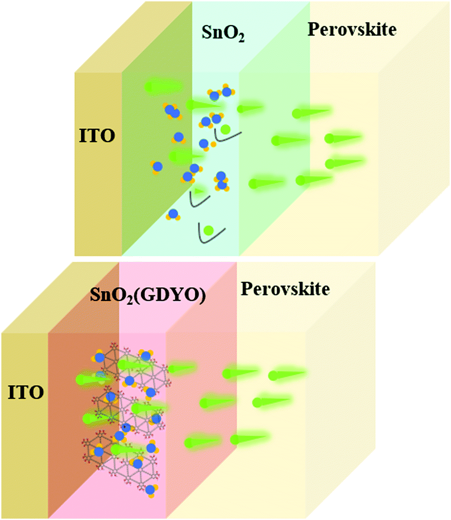
2. Results and discussion
Firstly, the properties of the SnO2 and GDYO-doped SnO2 were characterized to confirm the presence of GDYO in SnO2 and the associated interaction. To further investigate the interaction between GDYO and SnO2 nanoparticles, Raman spectroscopy was conducted, and the results are shown in Fig. S1 (ESI†). Fig. S1b (ESI†) exhibits that the prominent D band and G band peaks of sp2 carbon were located at ∼1362 cm−1 and ∼1582 cm−1, respectively.38 In the SnO2(GDYO) composites, the D band red shifted to a lower frequency region at ∼1324 cm−1, which reveals the interaction between GDYO and SnO2 nanoparticles. According to previous reports, the redshift can be attributed to the coupling between SnO2 nanoparticles and GDYO.39 Thus, we can assume that some chemical interaction between SnO2 and GDYO should be present. As is known, there are surface defects in the SnO2 ETL, which are mainly caused by oxygen vacancy defects formed by uncoordinated Sn on the surface. The existence of these defects seriously affects charge extraction and transport, and it leads to poor performance of perovskite photovoltaic devices. GDYO is oxidized and exfoliated from GDY and contains various functional groups, which are expected to inactivate the oxygen vacancy defects by bonding with the uncoordinated Sn.40Fig. 1a shows a schematic of the proposed interaction between the SnO2 surface and GDYO. It depicts the chemical bonding formation between the SnO2 surface and GDYO, where the uncoordinated Sn on the surface of SnO2 interacts with the carboxy and hydroxy groups in GDYO through chemical bonding. Fig. 1b shows the effect of this interaction, which could promote the electron transport. To demonstrate the interaction between GDYO and SnO2 nanoparticles, X-ray photoelectron spectroscopy (XPS) was carried out to explore the state of Sn and O elements in the SnO2(GDYO) and SnO2 films, respectively (Fig. S2, ESI†). As shown in Fig. 1c, the spectra of Sn 3d can be deconvoluted into peaks of 486.36 eV and 494.89 eV, which are in agreement with Sn 3d5/2 and Sn 3d3/2, respectively. Moreover, the peaks of Sn 3d shift slightly to higher binding energies for the SnO2(GDYO) film. Similar behavior of the O 1s peak for the SnO2(GDYO) film can be observed compared with that of the SnO2 film (Fig. 1d). The shift toward a higher binding energy indicates the presence of additional negative charges around Sn and O atoms. Furthermore, taking a closer look at Sn 3d5/2, two peaks appear at 486.4 eV and 486.8 eV, representing Sn2+ and Sn4+, respectively (Fig. 1e and f). The ratio of Sn4+ and Sn2+ peaks in the SnO2(GDYO) composite layer is larger than that in the SnO2 layer. It indicates that the density of the electron cloud around Sn increases with more Sn and O binding, and thus the oxygen-deficient defects are effectively passivated by GDYO. Meanwhile, we used XPS Gaussian distribution to conduct peak splitting treatment on O 1s to explore its valence state, vacancy and composition. According to Fig. S3 (ESI†), there are two oxygen states in the SnO2 film and SnO2(GDYO) film: 530.4 eV for the oxygen tin binding energy (O–Sn–O) and 531.4 eV for the oxygen vacancies energy. It was found that the proportion of O–Sn–O bonds was slightly increased by introducing GDYO in the SnO2 film, and the peak area of the oxygen vacancies decreased slightly. GDYO interacts with SnO2 to reduce the oxygen vacancy of SnO2, thus suppressing non-radiative recombination and promoting charge transport.8,41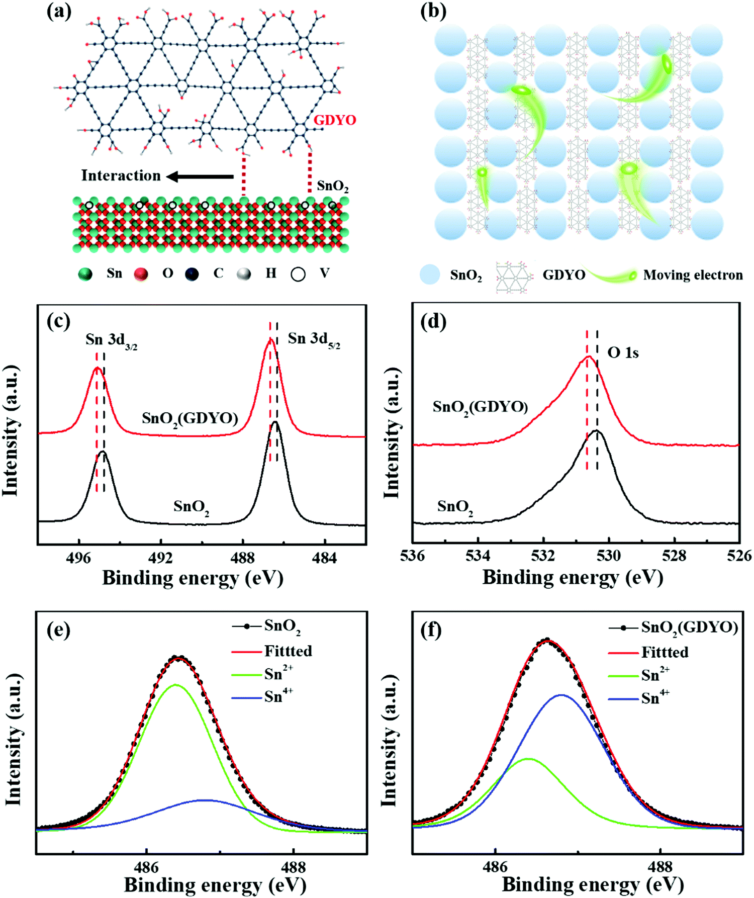 | ||
| Fig. 1 Schematic of (a) the proposed interaction between the SnO2 surface and GDYO and (b) the effect of GDYO doping in SnO2. The XPS spectra of (c) Sn 3d, (d) O 1s; XPS spectra of the Sn 3d5/2 peak measured from (e) the SnO2 layer and (f) the SnO2(GDYO) composite layer. | ||
The micro-morphology of the interface layer plays an important role in achieving high performance of PSCs. In order to understand how GDYO affects the microscopic features of SnO2 films, the dispersion solutions of the as-prepared SnO2(GDYO) composite and SnO2 were spin-coated on ITO, and the atomic force microscopy (AFM) results are shown in Fig. 2a–d and Fig. S4 (ESI†). As shown in Fig. 2c, the microscopic features of the SnO2(GDYO) film were significantly improved in comparison with those of the pure SnO2 film (Fig. 2a). The root-mean-square roughness (RMS) decreased from 2.51 nm to 2.01 nm after 2% GDYO doping, implying the formation of a smoother film. Therefore, GDYO modification can directly improve the microscopic features of the SnO2 surface, which will ultimately enhance the performance of PSCs.42 Fig. S5 (ESI†) shows the drop contact angles of the SnO2 and SnO2(GDYO) films. The slight change of the contact angle suggests that there is no significant difference in surface wettability. Furthermore, we performed top-view scanning electron microscopy (SEM) to examine the perovskite films on top of SnO2 and SnO2(GDYO) ETLs. As shown in Fig. 2e–h, it was noted that uniform, fully covered and hole-free perovskite layers with similar morphologies were obtained, but their grain sizes slightly differed. When the doping concentration of GDYO was 2%, the corresponding grain size reached its maximum. Consequently, the increase of grain size is beneficial to reducing grain boundary defects, thus suppressing non-radiative recombination and promoting carrier transport.43
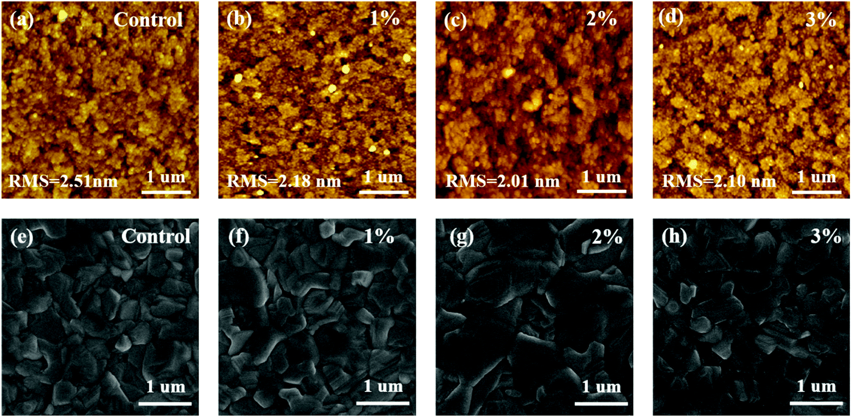 | ||
| Fig. 2 AFM images of (a) SnO2 and (b–d) SnO2(GDYO) ETLs with different doping concentrations. SEM images of perovskite films grown on (e) SnO2 ETL and (f–h) SnO2(GDYO) ETLs with different doping concentrations. The scale bar is 1 μm. | ||
The structure of the SnO2(GDYO)-based device, comprising ITO/SnO2(GDYO)/perovskite/spiro-OMeTAD/MoO3/Ag, is shown in Fig. 3a. The performance of perovskite devices is highly dependent on the optical properties of the adjacent ETLs. The transmission spectra of different ETLs were studied by UV-Vis spectroscopy. As shown in Fig. S6a (ESI†), the SnO2 and SnO2(GDYO) films show good light transmittance in the visible light range, which is advantageous for the perovskite film to absorb the incident light. Meanwhile, the band gaps (Eg) of these two films were calculated as 3.63 eV and 3.42 eV, respectively (Fig. S6b, ESI†). Normally, the energy level of ETL needs to be well matched with that of the perovskite layer, which determines the device performance, especially for VOC. To examine this, we studied the energy bands of the GDYO-free and GDYO-doped ETLs using ultraviolet photoelectron spectroscopy (UPS). The cutoff energy regions and the valence band maximum energy regions of the SnO2 and SnO2(GDYO) composite layers are depicted in Fig. S6c and d (ESI†). As shown in Fig. 3b, the valence band maxima (EV) of these ETLs are −7.45 eV (SnO2) and −7.48 eV (SnO2(GDYO)), respectively. Then, the corresponding conduction band minimum (EC) can be determined by the equation of EC = EV + Eg. EC values of −3.82 (SnO2) and −4.06 eV (SnO2(GDYO)) were obtained. Compared with the SnO2 film, EC of SnO2(GDYO) increased by 0.24 eV, suggesting that SnO2(GDYO) matches well with the energy level of the active layer; this will not only result in enhancement of the VOC, but also promote the extraction and injection of electrons and consequently improve the short-circuit current density (JSC) of the PSCs.44
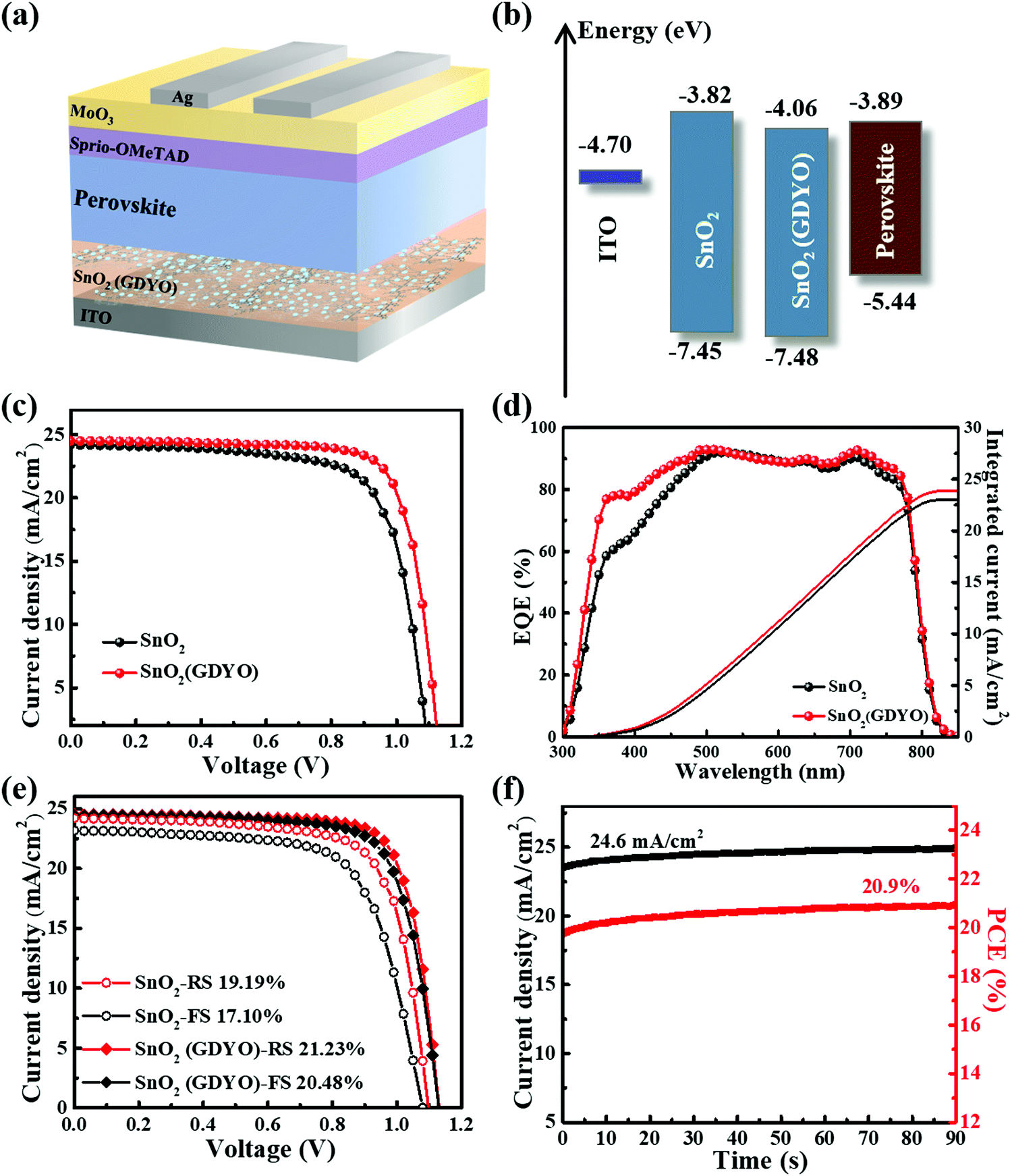 | ||
| Fig. 3 (a) Schematic of the device structure of SnO2(GDYO)-containing PSCs. (b) Diagram of the energy levels of the SnO2, SnO2(GDYO), and perovskite layers. (c) J–V curves, (d) EQE spectra and (e) J–V curves under reverse and forward scans of devices with and without GDYO modification. (f) Stabilized power output of the SnO2(GDYO)-based device. | ||
To evaluate the effect of SnO2 ETLs with and without GDYO on the photovoltaic performance, ITO/SnO2 or SnO2(GDYO) ETL/Perovskite/Spiro-OMeTAD/MoO3/Ag heterojunction cells were fabricated. Fig. 3c describes the corresponding J–V characteristics obtained under AM 1.5G irradiation (100 mW cm−2). The device with the pure SnO2 ETL exhibited a PCE of 19.19%, with a JSC of 24.20 mA cm−2, a VOC of 1.10 V, and a fill factor (FF) of 72.42%. In order to optimize device efficiency, varying GDYO doping concentrations were applied to SnO2. As shown in Fig. S7 (ESI†), the best PCE was obtained when the doping concentration of GDYO was 2%. The resultant device treated with GDYO yielded a peak PCE of 21.23% with a VOC of 1.13 V, a JSC of 24.49 mA cm−2, and an FF of 76.85%. Interestingly, it was found that the performance of all the GDYO-containing devices was superior to that of the control device. The better energy level arrangement and the reduction of defects in the SnO2/perovskite interface mainly account for the improved device performance. The corresponding EQE spectra are plotted in Fig. 3d. It can be observed that the whole spectrum is elevated in the visible light range, indicating higher extraction efficiency of the SnO2(GDYO)-based device (integrated current 23.91 mA cm−2) compared to that of the GDYO-free device (integrated current 23.06 mA cm−2). The EQE results of the SnO2(GDYO)-based device and control device concur with the J–V curves. In addition, as shown in Fig. 3e, the hysteresis of the SnO2(GDYO)-based device was obviously mitigated. The hysteresis index (HI) is used to evaluate the degree of hysteresis in accordance with the equation of HI = (PCEReverse − PCEForward)/PCEReverse,45 where PCEForward and PCEReverse represent the values of PCE during forward and reverse scanning, respectively. The HI values of devices based on the SnO2 and SnO2(GDYO) ETLs are 0.1 and 0.03, respectively. The hysteresis curve of J–V can be attributed to the presence of traps on the surface and the charge accumulation between the SnO2 layer and perovskite layer, as widely reported in the literature. After adding GDYO, the hysteresis can be significantly suppressed by reducing the trap state and effective electron extraction in the perovskite layer.
Fig. 3f shows the best steady-state power and photocurrent output device measured at its maximum power point (VMPP = 0.85 V). With the photocurrent stabilized at 24.6 mA cm−2, the PCE of the SnO2(GDYO)-based device can be retained at 20.9% for more than 90 s, consistent with the value extracted from the J–V curves. Besides, the GDYO-based device exhibited a narrow PCE distribution with a high average PCE, and the distribution of the other parameters fit a similar pattern (Fig. S8, ESI†).
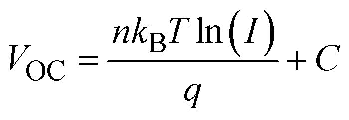
We measured the charge transfer properties in order to understand the effect of GDYO on improving the device performance. The mechanism of device recombination can be understood by determining the relationship between the photoelectric response and the intensity of incident light. It can be reflected by plotting VOC and JSC as functions of incident light intensity according to the following equations:
| J ∝ αI | (1) |
 | (2) |
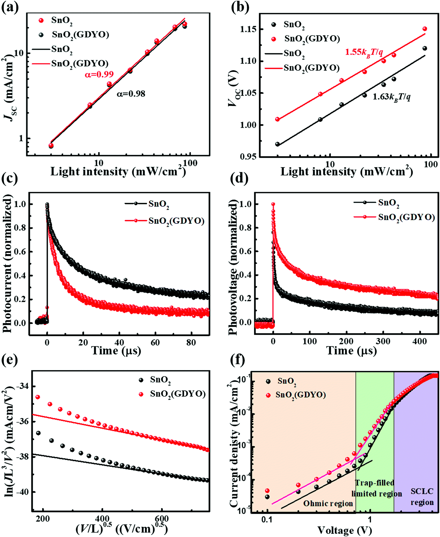 | ||
| Fig. 4 (a) JSC and (b) VOC dependence upon different light intensities of PSCs based on the SnO2 and SnO2(GDYO) ETLs. (c) Transient photocurrent decay curves and (d) transient photovoltage decay curves of PSCs based on SnO2 and SnO2(GDYO) ETLs. (e) J–V plotted in the format ln(JL3/V2) versus (V/L)0.5 for the device structure of ITO/Ag/SnO2/Ag or ITO/Ag/SnO2(GDYO)/Ag. (f) Dark J–V curves of electron-only devices based on the SnO2 and SnO2(GDYO) ETLs. | ||
In order to investigate the charge extraction ability upon doping GDYO, we also measured the transient photocurrent decay (TPC) and photovoltage decay (TPV) of the devices. As shown in Fig. 4c, the photocurrent decay time (transport time constants τt) of the device for SnO2(GDYO) was shorter than that of its counterpart (15.9 μs vs. 29.3 μs). Moreover, charge-recombination lifetime τr increased from 69.1 μs to 182.5 μs (Fig. 4d) after the addition of GDYO, which is indicative of more efficient charge extraction and reduced charge recombination.47 To further explore the carrier motility of the SnO2 and SnO2(GDYO) films, we measured the space charge limited conduction (SCLC) by using electron-only devices with the structures of ITO/Ag/SnO2/Ag and ITO/Ag/SnO2(GDYO)/Ag (Fig. 4e). The electron mobility of ETL films can be obtained by the field-independent Mott–Gurney equation:  , where J is the current density, ε0 is the permittivity of the vacuum, εr is the relative permittivity of SnO2, μ is the zero-field mobility of electrons, d is the thickness of the ETL, and V represents the applied potential to the device. Accordingly, the electron mobility of the pure SnO2-based electron-only device was 8.18 × 10⁻⁴ cm2 V−1 s−1, which is apparently lower than that of the SnO2(GDYO)-based counterpart (8.15 × 10⁻³ cm2 V−1 s−1). We attribute the increase of electron mobility to the highly electronic conductivity of GDYO. High electron mobility can accelerate electron transport which is critical to increase current.48
In addition, we conducted electrochemical impedance spectroscopy (EIS) analysis, as shown in Fig. S9 (ESI†). The diameter of a semicircle depicts the charge recombination resistance (Rrec), which is related to the leakage current and charge recombination of the perovskite layer and ETL. The SnO2(GDYO)-based device displayed a larger semicircle diameter than the control device, suggesting that less current leakage and electron recombination occurred at its surface. As a result, this facilitates the prevention of charge accumulation at the interface and improves the electron transfer efficiency.49
Electron-only devices with the structure of ITO/ETLs/perovskite/PCBM/Ag were fabricated in order to study the trap-state density at the interface of the perovskite and ETLs. Fig. 4f shows the corresponding J–V curves under dark conditions. The fitting curve consists of three regions: the ohmic region at low bias voltage, the trap-filling limited region, and the trap-free SCLC region at high voltage. The trap-state density Nt can be calculated by the trap-filled limit voltage using the following equation:
 | (3) |
Steady state photoluminescence spectroscopy (PL) was tested to further analyze the efficacy of doping GDYO in performance enhancement. Fig. 5a shows the photoluminescence spectra of a pristine perovskite film and the perovskite film deposited on SnO2 film and SnO2(GDYO) film, respectively. We measured the PL spectrum with an excitation light of 630 nm. The photoluminescence emission from perovskite at 790 nm is consistent with previous reports. Generally, a strong PL quenching indicates a high separation rate of photoexcited electron–hole pairs. Comparing the intensity of all peaks, a pronounced quenching effect was observed when GDYO was added to SnO2. This indicates that the SnO2(GDYO)-based device demonstrated higher electron extraction capability, which facilitates electron transport from perovskite to the ETL. The fast electronic transport capability can reduce the accumulation and charge recombination at the interface, which explains the enhancements in Jsc and FF.51
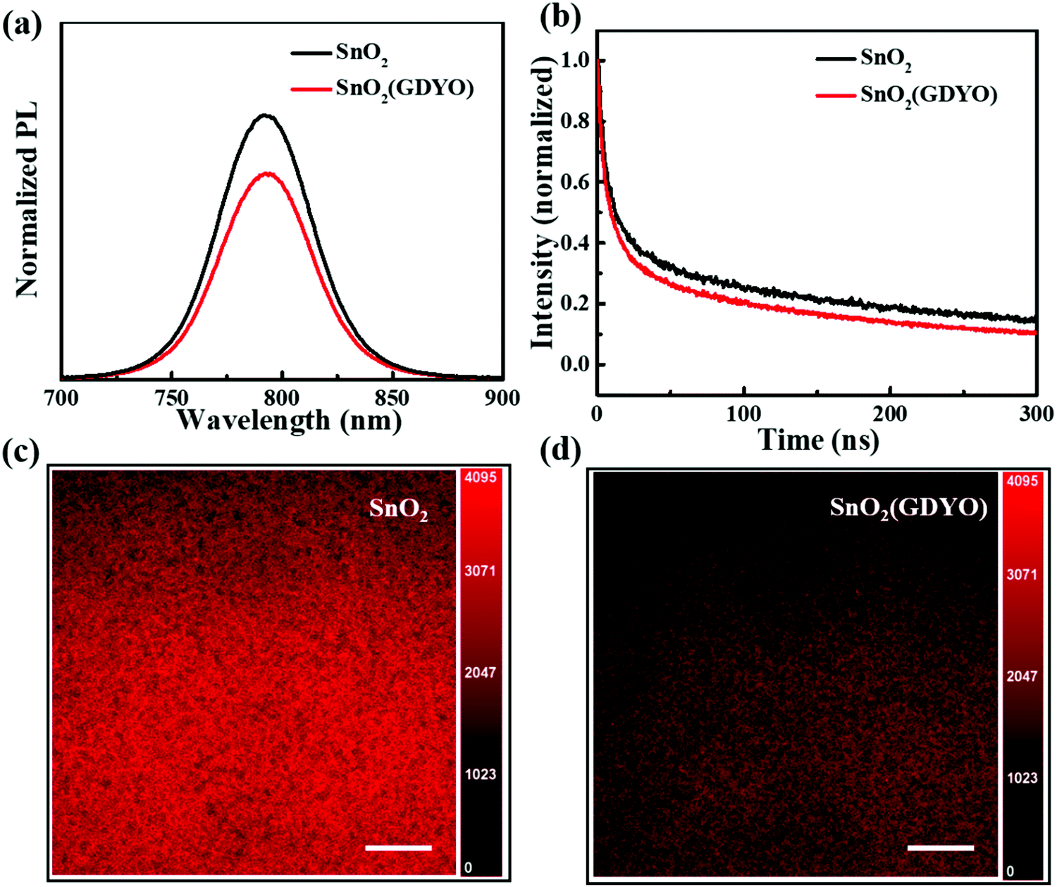 | ||
| Fig. 5 (a) Steady-state and (b) time-resolved photoluminescence spectra of perovskite films deposited on different substrates. Confocal fluorescence microscopy of perovskite films deposited on the (c) SnO2 ETL and (d) SnO2(GDYO) ETL; the scale bar is 1 μm. | ||
The time resolved photoluminescence (TRPL) was measured with the same device structure in order to elucidate the dynamic process of electron transfer and extraction. As shown in Fig. 5b, the data were fitted with two exponential decay curves to yield the lifetime of the carriers according to the equation of f(t) = A1![[thin space (1/6-em)]](https://www.rsc.org/images/entities/char_2009.gif) exp(−t/τ1) + A2exp(−t/τ2). The fast decay process (τ1) is mainly composed of bimolecular recombination of photo-generated free carriers, and the slow decay process (τ2) is produced by trap-assisted recombination; A1 and A2 represent the decay amplitude. Ultimately, the average decay time can be calculated, and the detailed parameters are listed in Table 1. The lifetimes obtained from TRPL measurements were 335.3 ns and 266.6 ns for the SnO2 and SnO2(GDYO) films, respectively. It was observed that the SnO2(GDYO) film showed a reduced PL lifetime, indicating that GDYO effectively enhanced the electronic extraction and transport capabilities of SnO2.52 Aiming to intuitively understand the carrier quenching dynamics, confocal fluorescence microscopy was used for characterization. As can be seen from Fig. 5c and d, the perovskite deposited on the SnO2(GDYO) film appeared darker than that on the SnO2 film, which is attributed to the efficient transport of carriers.53 This indicates that more carriers are transported to the transport layer instead of quenching on the perovskite surface after GDYO modification, which is consistent with the PL results. Fig. 6 shows the effect of GDYO doping on the electron transfer. There are many surface defects in the SnO2 ETL, which are mainly caused by oxygen vacancy defects formed by uncoordinated Sn on the surface. These defects can trap electrons and become the recombination centers of photogenerated carriers, thus seriously affecting the charge extraction and transport. GDYO can passivate these defects and promote carrier transport, which plays a positive role in improving the JSC and FF of the device and thus the overall performance of the device.
exp(−t/τ1) + A2exp(−t/τ2). The fast decay process (τ1) is mainly composed of bimolecular recombination of photo-generated free carriers, and the slow decay process (τ2) is produced by trap-assisted recombination; A1 and A2 represent the decay amplitude. Ultimately, the average decay time can be calculated, and the detailed parameters are listed in Table 1. The lifetimes obtained from TRPL measurements were 335.3 ns and 266.6 ns for the SnO2 and SnO2(GDYO) films, respectively. It was observed that the SnO2(GDYO) film showed a reduced PL lifetime, indicating that GDYO effectively enhanced the electronic extraction and transport capabilities of SnO2.52 Aiming to intuitively understand the carrier quenching dynamics, confocal fluorescence microscopy was used for characterization. As can be seen from Fig. 5c and d, the perovskite deposited on the SnO2(GDYO) film appeared darker than that on the SnO2 film, which is attributed to the efficient transport of carriers.53 This indicates that more carriers are transported to the transport layer instead of quenching on the perovskite surface after GDYO modification, which is consistent with the PL results. Fig. 6 shows the effect of GDYO doping on the electron transfer. There are many surface defects in the SnO2 ETL, which are mainly caused by oxygen vacancy defects formed by uncoordinated Sn on the surface. These defects can trap electrons and become the recombination centers of photogenerated carriers, thus seriously affecting the charge extraction and transport. GDYO can passivate these defects and promote carrier transport, which plays a positive role in improving the JSC and FF of the device and thus the overall performance of the device.
| Samples | τ 1 (ns) | A 1 | τ 2 (ns) | A 2 | τ ave (ns) |
|---|---|---|---|---|---|
| SnO2 | 12.59 | 0.394 | 344.9 | 0.482 | 335.3 |
| SnO2(GDYO) | 10.44 | 0.619 | 287.4 | 0.297 | 266.6 |
 | ||
| Fig. 6 Schematic of the effect of GDYO doping of SnO2. | ||
The thermal and illumination stability of the SnO2 and SnO2(GDYO)-based devices were tested with poly(triarylamine) (PTAA) replacing spiro-OMeTAD as the hole transport material. The initial PCEs of the SnO2 and SnO2(GDYO)-based devices with a PTAA hole transport layer were 15.1% and 17.6%, respectively (Fig. S10, ESI†). As shown in Fig. S11a (ESI†), the thermal stability test was carried out in a nitrogen box with heating at 80 °C; over 80% of the initial value of the GDYO-based device was retained after 25 days, which was much better than the control device. We also tracked the light stability under 1 sun illumination (25 °C, under nitrogen storage), and the GDYO-based device also showed better stability (Fig. S11b, ESI†). The stability tests indicate that GDYO modification of a SnO2 ETL is an effective approach to improve device stability. The interaction between GDYO and SnO2, associated with reduced oxygen vacancy defects, improved the carrier transport efficiency and reduced the charge recombination, consequently contributing to the improved device stability.
3. Conclusion
To conclude, we have introduced an effective interface engineering approach for a high-performance planar PSC by using a novel SnO2(GDYO) ETL. It is demonstrated that the terminal carboxy and hydroxy groups of GDYO can link the uncoordinated Sn in SnO2via chemical bonds, leading to reduced oxygen vacancy of SnO2; this further facilitates the suppression of the non-radiative recombination and promotes the charge transport. Upon the incorporation of GDYO, the quality of both the SnO2 film and perovskite film was improved. As a result, the SnO2(GDYO)-based device achieved a high PCE of 21.23%, which is an enhancement of over 10% as compared to the control device. Furthermore, the device stability was improved. The SnO2(GDYO)-based device maintained 71% of its initial PCE after 160 h under continuous illumination and 84% after 24 days of heating at 80 °C. These findings highlight the significance of precise interface engineering toward high-performance PSCs and extend the promising applications of functionalized GDY in photovoltaic technologies.Conflicts of interest
There are no conflicts of interest to declare.Acknowledgements
This work was supported by National Natural Science Foundation of China (No. 21975273), Scientific Research Starting Foundation of Outstanding Young Scholar of Shandong University, the Fundamental Research Funds of Shandong University, and Dalian National Laboratory For Clean Energy (DICP & QIBEBT UN201705).Notes and references
- D. H. Ahn, S. W. Kim, H. Lee, I. J. Ko, D. Karthik, J. Y. Lee and J. H. Kwon, Highly efficient blue thermally activated delayed fluorescence emitters based on symmetrical and rigid oxygen-bridged boron acceptors, Nat. Photonics, 2019, 13, 540–546 CrossRef CAS
.
- S. Yakunin, D. N. Dirin, Y. Shynkarenko, V. Morad, I. Cherniukh, O. Nazarenko, D. Kreil, T. Nauser and M. V. Kovalenko, Detection of gamma photons using solution-grown single crystals of hybrid lead halide perovskites, Nat. Photonics, 2016, 10, 585–589 CrossRef CAS
- H. M. Gwisu Kim, K. Su Lee, D. Yoon Lee, S. Me Yoon and S. Il Seok, Impact of strain relaxation on performance of a-formamidinium lead iodide perovskite solar cells, Science, 2020, 370, 108–112 CrossRef PubMed
- NREL, Best Research-cell Efficiency Chart, 2020, https://www.nrel.gov/pv/cell-efficiency.html.
- A. Kojima, K. Teshima, Y. Shirai and T. Miyasaka, Organometal halide perovskites as visible-light sensitizers for photovoltaic cells, J. Am. Chem. Soc., 2009, 131, 6050–6051 CrossRef CAS
- G. Yang, H. Tao, P. Qin, W. Ke and G. Fang, Recent progress in electron transport layers for efficient perovskite solar cells, J. Mater. Chem. A, 2016, 4, 3970–3990 RSC
- M. L. Petrus, J. Schlipf, C. Li, T. P. Gujar, N. Giesbrecht, P. Müller-Buschbaum, M. Thelakkat, T. Bein, S. Hüttner and P. Docampo, Capturing the sun: a review of the challenges and perspectives of perovskite solar cells, Adv. Energy Mater., 2017, 7, 1700264 CrossRef
- H. Tan, A. Jain, O. Voznyy, X. Lan, F. P. García de Arquer, J. Z. Fan, R. Quintero-Bermudez, M. Yuan, B. Zhang, Y. Zhao, F. Fan, P. Li, L. N. Quan, Y. Zhao, Z.-H. Lu, Z. Yang, S. Hoogland and E. H. Sargent, Efficient and stable solution-processed planar perovskite solar cells via contact passivation, Science, 2017, 355, 722 CrossRef CAS PubMed
- E. H. Anaraki, A. Kermanpur, L. Steier, K. Domanski, T. Matsui, W. Tress, M. Saliba, A. Abate, M. Grätzel, A. Hagfeldt and J.-P. Correa-Baena, Highly efficient and stable planar perovskite solar cells by solution-processed tin oxide, Energy Environ. Sci., 2016, 9, 3128–3134 RSC
- W.-Q. Wu, D. Chen, R. A. Caruso and Y.-B. Cheng, Recent progress in hybrid perovskite solar cells based on n-type materials, J. Mater. Chem. A, 2017, 5, 10092–10109 RSC
- N. J. Jeon, H. Na, E. H. Jung, T.-Y. Yang, Y. G. Lee, G. Kim, H.-W. Shin, S. Il Seok, J. Lee and J. Seo, A fluorene-terminated hole-transporting material for highly efficient and stable perovskite solar cells, Nat. Energy, 2018, 3, 682–689 CrossRef CAS
- J. A. Christians, P. Schulz, J. S. Tinkham, T. H. Schloemer, S. P. Harvey, B. J. Tremolet de Villers, A. Sellinger, J. J. Berry and J. M. Luther, Tailored interfaces of unencapsulated perovskite solar cells for >1000 hour operational stability, Nat. Energy, 2018, 3, 68–74 CrossRef CAS
- Y. Wang, J. Wan, J. Ding, J. Hu and D. Wang, A rutile TiO2 electron transport layer for the enhancement of charge collection for efficient perovskite solar cells, Angew. Chem., Int. Ed., 2019, 58, 9414–9418 CrossRef CAS
- T. Leijtens, G. E. Eperon, S. Pathak, A. Abate, M. M. Lee and H. J. Snaith, Overcoming ultraviolet light instability of sensitized TiO2 with meso-superstructured organometal tri-halide perovskite solar cells, Nat. Commun., 2013, 4, 2885 CrossRef PubMed
- Q. Jiang, X. Zhang and J. You, SnO2: a wonderful electron transport layer for perovskite solar cells, Small, 2018, 14, 1801154 CrossRef
- H. Sun, J. Deng, L. Qiu, X. Fang and H. Peng, Recent progress in solar cells based on one-dimensional nanomaterials, Energy Environ. Sci., 2015, 8, 1139–1159 RSC
- F. Gao, Y. Zhao, X. Zhang and J. You, Recent progresses on defect passivation toward efficient perovskite solar cells, Adv. Energy Mater., 2020, 10, 1902650 CrossRef CAS
- T. Bu, J. Li, F. Zheng, W. Chen, X. Wen, Z. Ku, Y. Peng, J. Zhong, Y. B. Cheng and F. Huang, Universal passivation strategy to slot-die printed SnO2 for hysteresis-free efficient flexible perovskite solar module, Nat. Commun., 2018, 9, 4609 CrossRef
- M. Acik and S. B. Darling, Graphene in perovskite solar cells: device design, characterization and implementation, J. Mater. Chem. A, 2016, 4, 6185–6235 RSC
- Z. Saki, K. Aitola, K. Sveinbjörnsson, W. Yang, S. Svanström, U. B. Cappel, H. Rensmo, E. M. J. Johansson, N. Taghavinia and G. Boschloo, The synergistic effect of dimethyl sulfoxide vapor treatment and C60 electron transporting layer towards enhancing current collection in mixed-ion inverted perovskite solar cells, J. Power Sources, 2018, 405, 70–79 CrossRef CAS
- S. N. Habisreutinger, T. Leijtens, G. E. Eperon, S. D. Stranks, R. J. Nicholas and H. J. Snaith, Carbon nanotube/polymer composites as a highly stable hole collection layer in perovskite solar cells, Nano Lett., 2014, 14, 5561–5568 CrossRef CAS PubMed
- Z. Jia, Y. Li, Z. Zuo, H. Liu, C. Huang and Y. Li, Synthesis and properties of 2D carbon-graphdiyne, Acc. Chem. Res., 2017, 50, 2470–2478 CrossRef CAS
- S. Zhan, Y. Zhao, N. Yang and D. Wang, Pore structure of graphdiyne: design, synthesis and application, Chem. J. Chin. Univ., 2021, 42, 333–348 Search PubMed
- Y. Zhao, N. Yang, R. Yu, Y. Zhang, J. Zhang and Y. Li,
et al., Unique structural advances of graphdiyne for energy applications, EnergyChem, 2020, 100041 CrossRef
- C. Xing, Y. Xue, B. Huang, H. Yu, L. Hui, Y. Fang, Y. Liu, Y. Zhao, Z. Li and Y. Li, Fluorographdiyne: a metal-free catalyst for applications in water reduction and oxidation, Angew. Chem., Int. Ed., 2019, 58, 13897–13903 CrossRef CAS PubMed
- N. Wang, J. He, Z. Tu, Z. Yang, F. Zhao, X. Li, C. Huang, K. Wang, T. Jiu, Y. Yi and Y. Li, Synthesis of chlorine-substituted graphdiyne and applications for lithium-ion storage, Angew. Chem., Int. Ed., 2017, 56, 10740–10745 CrossRef CAS PubMed
- H. Shang, Z. Zuo, L. Li, F. Wang, H. Liu, Y. Li and Y. Li, Ultrathin graphdiyne nanosheets grown in situ on copper nanowires and their performance as lithium-ion battery anodes, Angew. Chem., Int. Ed., 2018, 57, 774–778 CrossRef CAS
- Y. Fang, Y. Xue, L. Hui, H. Yu and Y. Li, Graphdiyne@Janus magnetite for photocatalytic nitrogen fixation, Angew. Chem., Int. Ed., 2021, 60, 3170–3174 CrossRef CAS
- J. Li, C. Wan, C. Wang, H. Zhang and X. Chen, 2D material chemistry: graphdiyne-based biochemical sensing, Chem. Res. Chin. Univ., 2020, 36, 622–630 CrossRef CAS
- C. Yang, H. F. Wang and Q. Xu, Recent advances in two-dimensional materials for electrochemical energy storage and conversion, Chem. Res. Chin. Univ., 2020, 36, 10–23 CrossRef CAS
- Y. Fang, Y. Xue, Y. Li, H. Yu, L. Hui, Y. Liu, C. Xing, C. Zhang, D. Zhang, Z. Wang, X. Chen, Y. Gao, B. Huang and Y. Li, Graphdiyne interface engineering: highly active and selective ammonia synthesis, Angew. Chem., Int. Ed., 2020, 59, 13021–13027 CrossRef CAS
- F. Wang, Z. Zuo, L. Li, K. Li, F. He, Z. Jiang and Y. Li, Large-area aminated-graphdiyne thin films for direct methanol fuel cells, Angew. Chem., Int. Ed., 2019, 58, 15010–15015 CrossRef CAS
- N. Wang, X. Li, Z. Tu, F. Zhao, J. He, Z. Guan, C. Huang, Y. Yi and Y. Li, Synthesis and electronic structure of boron-graphdiyne with an sp-hybridized carbon skeleton and its application in sodium storage, Angew. Chem., Int. Ed., 2018, 57, 3968–3973 CrossRef CAS PubMed
- M. Li, Z.-K. Wang, T. Kang, Y. Yang, X. Gao, C.-S. Hsu, Y. Li and L.-S. Liao, Graphdiyne-modified cross-linkable fullerene as an efficient electron-transporting layer in organometal halide perovskite solar cells, Nano Energy, 2018, 43, 47–54 CrossRef CAS
- C. Kuang, G. Tang, T. Jiu, H. Yang, H. Liu, B. Li, W. Luo, X. Li, W. Zhang, F. Lu, J. Fang and Y. Li, Highly efficient electron transport obtained by doping PCBM with graphdiyne in planar-heterojunction perovskite solar cells, Nano Lett., 2015, 15, 2756–2762 CrossRef CAS
- J. Li, M. Zhao, C. Zhao, H. Jian, N. Wang, L. Yao, C. Huang, Y. Zhao and T. Jiu, Graphdiyne-Doped P3CT-K as an Efficient hole-transport layer for MAPbI3 perovskite solar cells, ACS Appl. Mater. Interfaces, 2019, 11, 2626–2631 CrossRef CAS
- T. Zheng, Y. Gao, X. Deng, H. Liu, J. Liu, R. Liu, J. Shao, Y. Li and L. Jia, Comparisons between Graphene Oxide and Graphdiyne Oxide in Physicochemistry Biology and Cytotoxicity, ACS Appl. Mater. Interfaces, 2018, 10, 32946–32954 CrossRef CAS
- X. Gao, J. Zhou, R. Du, Z. Xie, S. Deng, R. Liu, Z. Liu and J. Zhang, Robust superhydrophobic foam: a graphdiyne-based hierarchical architecture for oil/water separation, Adv. Mater., 2016, 28, 168–173 CrossRef CAS PubMed
- J. Li, H. Jian, Y. Chen, H. Liu, L. Liu, Q. Yao, F. Bi, C. Zhao, X. Tan, J. Jiang, F. Lu and T. Jiu, Studies of graphdiyne-ZnO nanocomposite material and application in polymer solar cells, Sol. RRL, 2018, 2, 1800211 CrossRef
- K. Liu, S. Chen, J. Wu, H. Zhang, M. Qin, X. Lu, Y. Tu, Q. Meng and X. Zhan, Fullerene derivative anchored SnO2 for high-performance perovskite solar cells, Energy Environ. Sci., 2018, 11, 3463–3471 RSC
- M. Batzill and U. Diebold, The surface and materials science of tin oxide, Prog. Surf. Sci., 2005, 79, 47–154 CrossRef CAS
- P. You, Z. Liu, Q. Tai, S. Liu and F. Yan, Efficient semitransparent perovskite solar cells with graphene electrodes, Adv. Mater., 2015, 27, 3632–3638 CrossRef CAS
- C. Bi, Q. Wang, Y. Shao, Y. Yuan, Z. Xiao and J. Huang, Non-wetting surface-driven high-aspect-ratio crystalline grain growth for efficient hybrid perovskite solar cells, Nat. Commun., 2015, 6, 7747 CrossRef CAS PubMed
- K. Lu, Y. Lei, R. Qi, J. Liu, X. Yang, Z. Jia, R. Liu, Y. Xiang and Z. Zheng, Fermi level alignment by copper doping for efficient ITO/perovskite junction solar cells, J. Mater. Chem. A, 2017, 5, 25211–25219 RSC
- S. N. Habisreutinger, N. K. Noel and H. J. Snaith, Hysteresis index: a figure without merit for quantifying hysteresis in perovskite solar cells, ACS Energy Lett., 2018, 3, 2472–2476 CrossRef CAS
- D. Yang, X. Zhou, R. Yang, Z. Yang, W. Yu, X. Wang, C. Li, S. Liu and R. P. H. Chang, Surface optimization to eliminate hysteresis for record efficiency planar perovskite solar cells, Energy Environ. Sci., 2016, 9, 3071–3078 RSC
- Q. Jiang, L. Zhang, H. Wang, X. Yang, J. Meng, H. Liu, Z. Yin, J. Wu, X. Zhang and J. You, Enhanced electron extraction using SnO2 for high-efficiency planar-structure HC(NH2)2PbI3-based perovskite solar cells, Nat. Energy, 2016, 2, 161777 Search PubMed
- Z. Tan, W. Zhang, Z. Zhang, D. Qian, Y. Huang, J. Hou and Y. Li, High-performance inverted polymer solar cells with solution-processed titanium chelate as electron-collecting layer on ITO electrode, Adv. Mater., 2012, 24, 1476–1481 CrossRef CAS PubMed
- J. Li, T. Jiu, B. Li, C. Kuang, Q. Chen, S. Ma, J. Shu and J. Fang, Inverted polymer solar cells with enhanced fill factor by inserting the potassium stearate interfacial modification layer, Appl. Phys. Lett., 2016, 108, 181602 CrossRef
- S. Chen, Q. Pan, J. Li, C. Zhao, X. Guo, Y. Zhao and T. Jiu, Grain boundary passivation with triazine-graphdiyne to improve perovskite solar cell performance, Sci. China Mater., 2020, 63, 2465–2476 CrossRef
- L. L. Jiang, Z.-K. Wang, M. Li, C. H. Li, P. F. Fang and L. S. Liao, Enhanced electrical property of compact TiO2 layer via platinum doping for high-performance perovskite solar cells, Sol. RRL, 2018, 2, 1800149 CrossRef
- Q. Liu, X. Zhang, C. Li, H. Lu, Z. Weng, Y. Pan, W. Chen, X. C. Hang, Z. Sun and Y. Zhan, Effect of tantalum doping on SnO2 electron transport layer via low temperature process for perovskite solar cells, Appl. Phys. Lett., 2019, 115, 143903 CrossRef
- H. C. Cheng, G. Wang, D. Li, Q. He, A. Yin, Y. Liu, H. Wu, M. Ding, Y. Huang and X. Duan, van der Waals heterojunction devices based on organohalide perovskites and two-dimensional materials, Nano Lett., 2016, 16, 367–373 CrossRef CAS PubMed
Footnotes |
| † Electronic supplementary information (ESI) available. See DOI: 10.1039/d1qm00592h |
| ‡ These authors contributed equally to this work. |
| This journal is © the Partner Organisations 2021 |